
Thin Film Deposition of MoP, a Topological Semimetal

Department of Physics, Portland State University, Portland, OR 97207, USA
*
Author to whom correspondence should be addressed.
Appl. Nano 2023, 4(1), 38-44; https://doi.org/10.3390/applnano4010003
Submission received: 30 January 2023
/
Revised: 10 February 2023
/
Accepted: 20 February 2023
/
Published: 24 February 2023
(This article belongs to the Collection Feature Papers for Applied Nano)
Abstract
:MoP is a topological semimetal which has drawn attention due to its unique electrical and optical properties resulting from massless electrons. In order to utilize these properties for practical applications, it is necessary to develop a technique to produce high-quality, large-scale thin films of this 2D material. We report below our initial results of growth of MoP thin films using atomic layer deposition (ALD), where the film grows layer-by-layer. These films were grown on 5 cm × 5 cm silicon oxide coated Si wafers. Resistivity versus temperature measurements show that these films are metallic and includes a partial superconducting phase. The magnetoresistances of both the longitudinal and Hall currents measured at 1.8 K show a strong effect of the magnetic field on the resistivity. Density functional theory was employed to determine the lattice constants of the MoP crystal. These parameters were in good agreement with those obtained from the Rietveld fit to the XRD spectrum of the films.
1. Introduction
Conventional metals and insulators have been routinely used to fabricate electronic devices since their inception; however, the topological form of these materials has recently opened up a whole new frontier. These topological materials have surface states which are induced by the inversion of the bulk band structure, which give rise to spin-polarized electronic states with linear energy–momentum dispersion at their edge or surface [1,2]. In the case of topological insulators (TI), band inversion leads to metallic surface states where spin and momentum are fixed and perpendicular to each other [1,2,3]. Therefore, electrons carrying opposite spins propagate in opposite directions which, in principle, should prevent the backscattering that requires the electrons to flip their spin. Similar surface states also exist in topological semimetals (TS); however, unlike TI, which may retain only a few residual bulk carriers, topological metals retain their bulk carriers, thereby maintaining their metallic character [1,3]. In order to utilize these properties in practical devices, the first step is to be able to produce films of this material over wafer scale areas. In this communication, we describe our initial results of a technique used to grow uniform, thin films of MoP, a topological semimetal (TS) over large areas, and we present some of the properties of these thin films.
TS are grouped as either Dirac or Weyl. MoP is a Weyl semimetal, which is characterized by topological Fermi arcs on the surface and chiral magnetic effects in the bulk [4,5,6]. Weyl semimetals with spontaneously broken time-reversal symmetry exhibit a large intrinsic anomalous Hall effect originating from the Berry curvature [7,8]. MoP is a 2D material, and it has low resistivity and high carrier density; hence, it has attracted special attention as a replacement for Cu interconnects in semiconductor devices at the sub-7nm technology node [5,9,10,11]. Factors leading to low resistivity in this semimetal are the linear dispersion and spin momentum locking at the topologically protected surface states that could suppress electron backscattering from the Cu grain boundaries and other imperfections in the damascened interconnects [5,9,12]. Moreover, it has been shown that contrary to conventional conductors, the resistance of MoP nanowires decreases with the reduction in the nanowire diameter [13]. This new class of quantum materials is particularly suitable for nanoscale electronic devices where the topological states can be enhanced because of their large surface-to-volume ratios. MoP films have also been shown to be effective catalysts for hydrogen evolution reactions [14,15].
2. Materials and Methods
Ideally, a technique for growing a new material for microelectronic devices should be compatible with the existing fabrication process. To date, a few methods have been reported for the growth of MoP thin films. The most common growth technique is to replace the chalcogenide of either MoO2 or MoS2 films with P by reacting them with PH3 [16,17]. There is also a report describing MoP growth using chemical vapor deposition on liquid metals [14]. For most electronic applications of MoP, it will be preferable to grow thin films of this material on large area silicon substrates. To employ the large Hall current for room-temperature topo-spintronics applications, it is necessary to fabricate these materials as thin or ultrathin films. One of the possible techniques that enables such fabrication is atomic layer deposition (ALD). The MoP films reported below were grown on SiO2-coated silicon substrates using ALD. ALD is a stepwise growth process where the precursors are alternately injected into the growth area; following each reaction, excess species and by-products are removed with an inert gas (). As a result, uniform, high quality films are grown over large areas by sequential self-limiting surface reactions [18]. This process enables precise control of the film composition and thickness as the growth proceeds layer by layer. We previously utilized this technique for the growth of other 2D semiconductors, including , a topological insulator [19]. All these films have been grown in a Microchemistry F-120 reactor which can hold two 5 cm × 5 cm substrates per run. The substrates for MoP films consisted of n-type Si wafers coated with a 320-nm-thick layer of thermal silicon oxide. Since film growth occurs via van der Waals epitaxy, lattice-matched substrates are not required [20]. The precursors for MoP growth were and (5% , balance ). A hot wire was used in the channel for its decomposition that facilitated film growth at a lower temperature. The Mo source temperature was set at 98 °C, and the carrier gas was nitrogen. The pulse sequence per cycle was as follows: pulse width of 1.0 s; purge of 1.2 s; and pulse width of 5 s; followed by 1.2 s purge. Uniform films at a constant growth rate were obtained over a temperature range of 390 °C to 440 °C, which defined the ALD growth window. The films reported here were grown at 400 °C, where the growth rate was 0.2 nm per cycle. This growth technique does not require a “wetting” layer on the substrate since the growth mechanism starts with the surface saturated with a chemisorbed layer of the reacting species [18].
The constant growth rate (growth/cycle) within the ALD window was determined by optimizing the process parameters such as the temperature, pulse widths, and flow rates. Energy dispersive spectroscopy (EDS) analysis was used to determine the stoichiometry of these films. Films grown within the ALD temperature window had a Mo:P atomic ratio of close to 1:1 (P atomic % = 48.34, Mo atomic % = 51.66).
3. Results and Discussion
3.1. DFT Studies
Open-source plane wave Density Functional Theory (DFT) program Quantum Espresso was used to compute the density of states (DOS), band diagram, and the lattice constants of hexagonal MoP. The electronic structure of MoP was calculated using the fully relativistic Perdew–Burke–Ernzerhof (PBE) ultra-soft pseudopotentials [21]. A plane wave cut-off of 48.95 Rydbergs and Fermi smearing of 0.001 Rydbergs. A k-mesh of 9 × 9 × 4 was used for the electron calculations. The crystal of hexagonal MoP produced from the simulation structure is shown in Figure 1. The lattice constants and angles determined from the simulation are a = b = 0.322 nm and c = 0.319 nm, and the angles were 90, 90, and 120 degrees, respectively. These parameters are consistent with those reported in the literature [14].
3.2. Crystallographic Properties
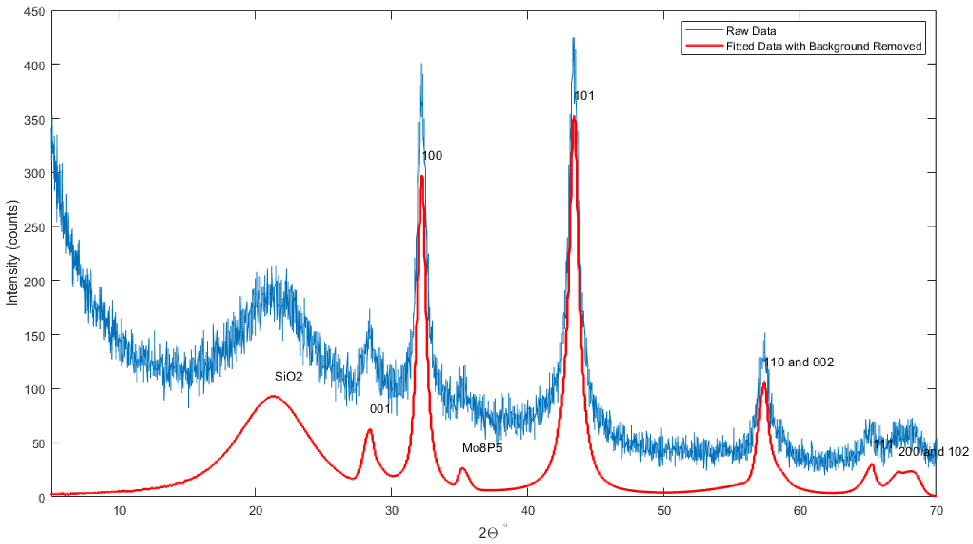
The crystalline properties of these thin films were examined using grazing incidence (0.5) X-ray diffraction (XRD). The XRD pattern of a 24 nm thick MoP film is shown in Figure 2.
The XRD plot shows peaks at 28.0, 32.2, 43.1, 57.2, 65, and 67.4, which have been reported previously for the hexagonal phase of MoP; the results are also in agreement with JCPDS (24-771) diffraction data [22,23]. In addition to the MoP peaks, two weaker peaks were also recorded. These additional peaks were found to belong to the phase of molybdenum phosphide (JCPDS 26-1274). Formation of under high pressure has been reported previously [24]; however, the ALD process is a non-equilibrium growth process (flowing only one source at a time), unlike conventional growth processes. Hence, presence of the in ALD growth is not surprising.
The XRD pattern indicates that the MoP film is oriented along the c-axis. The broad peak at around 23 degrees is from the underlying amorphous film of the substrate [25]. The Rietveld curve fit of this x-ray spectrum with FullProf software was used to remove the background and extract the lattice parameters. The lattice parameters extracted were a = b = 0.322 nm and c = 0.318 nm of the hexagonal phase, where the angles were 90, 90, and 120 degrees, respectively. These values are in close agreement with the lattice constants and angles extracted from our DFT simulation, which were a = b = 0.323 nm and c = 0.321 nm. To rule out the formation of terraces and other growth defects, we examined a sample surface with a scanning electron microscope (SEM). The SEM analysis did not reveal any texture indicating absence of major defects in the grown films. The SEM image is provided in the Supplementary Materials.
3.3. Transport Properties
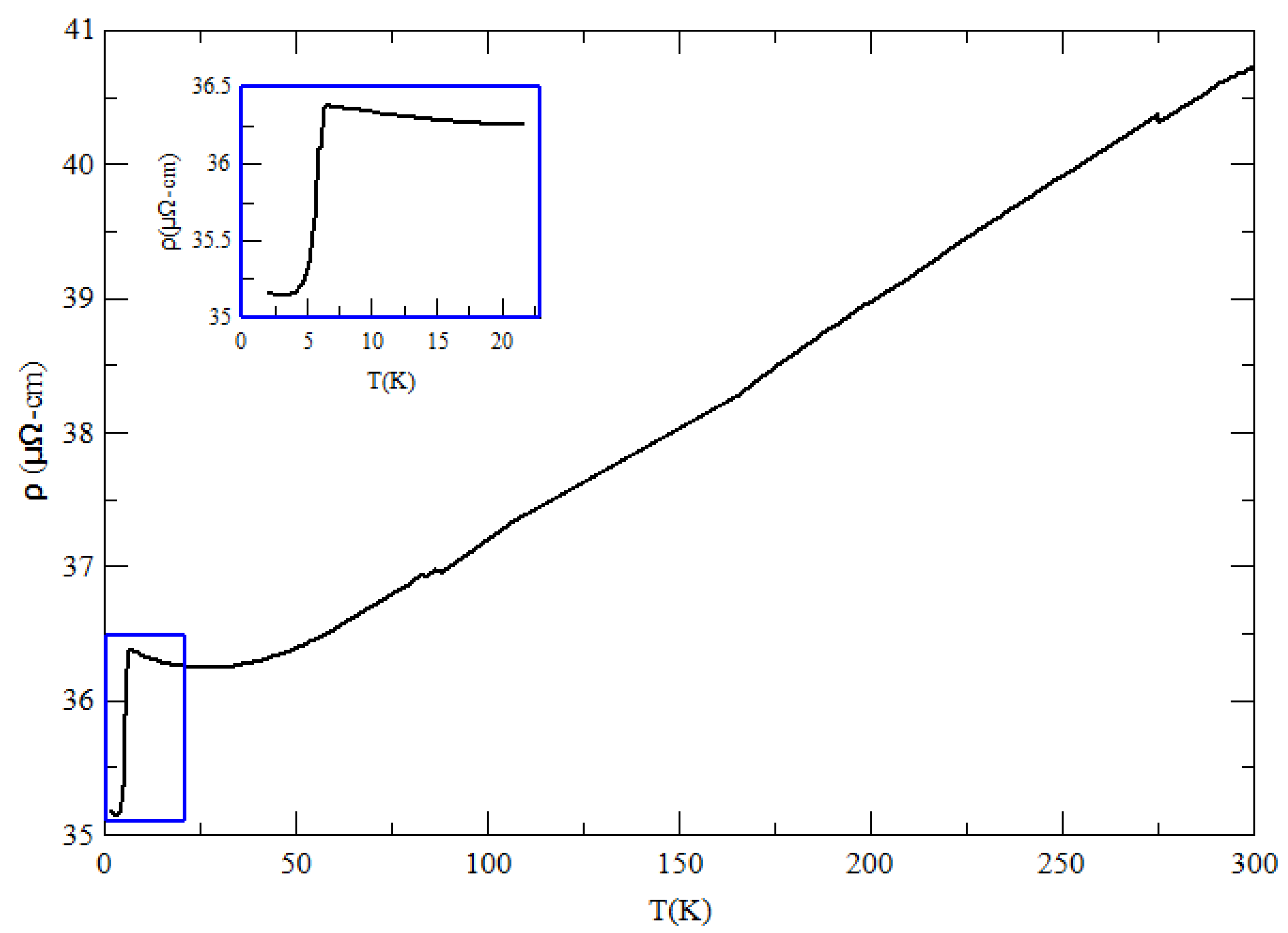
The transport properties of carriers were examined using samples of approximately 1 cm × 1 cm that were cleaved from larger substrates. The film thickness of these samples was 24 nm. Indium solder was used to connect Cu wires along the edge of these substrates in a Hall bridge configuration. First, the longitudinal resistivity () of the film was measured versus the temperature, as shown in Figure 3. As expected, the resistivity of the film decreased as the temperature was lowered, indicating a metallic film. It is interesting to note that at about 6 K, there was a sharp drop in resistivity, but it did not reach zero. This feature was repeatable and we believe this indicates the presence of a partial superconducting phase. This TC temperature is in agreement with the TC value of (5.8 K) that was reported for in [24]. From the XRD data, it is clear that the amount of the phase comprises only a small fraction of the sample; therefore, the residual resistance is attributed to non-superconductive MoP (TC = 1 K) and indium (TC = 3.4 K), which was used to contact the wires with the sample.
3.4. Magnetoresitance
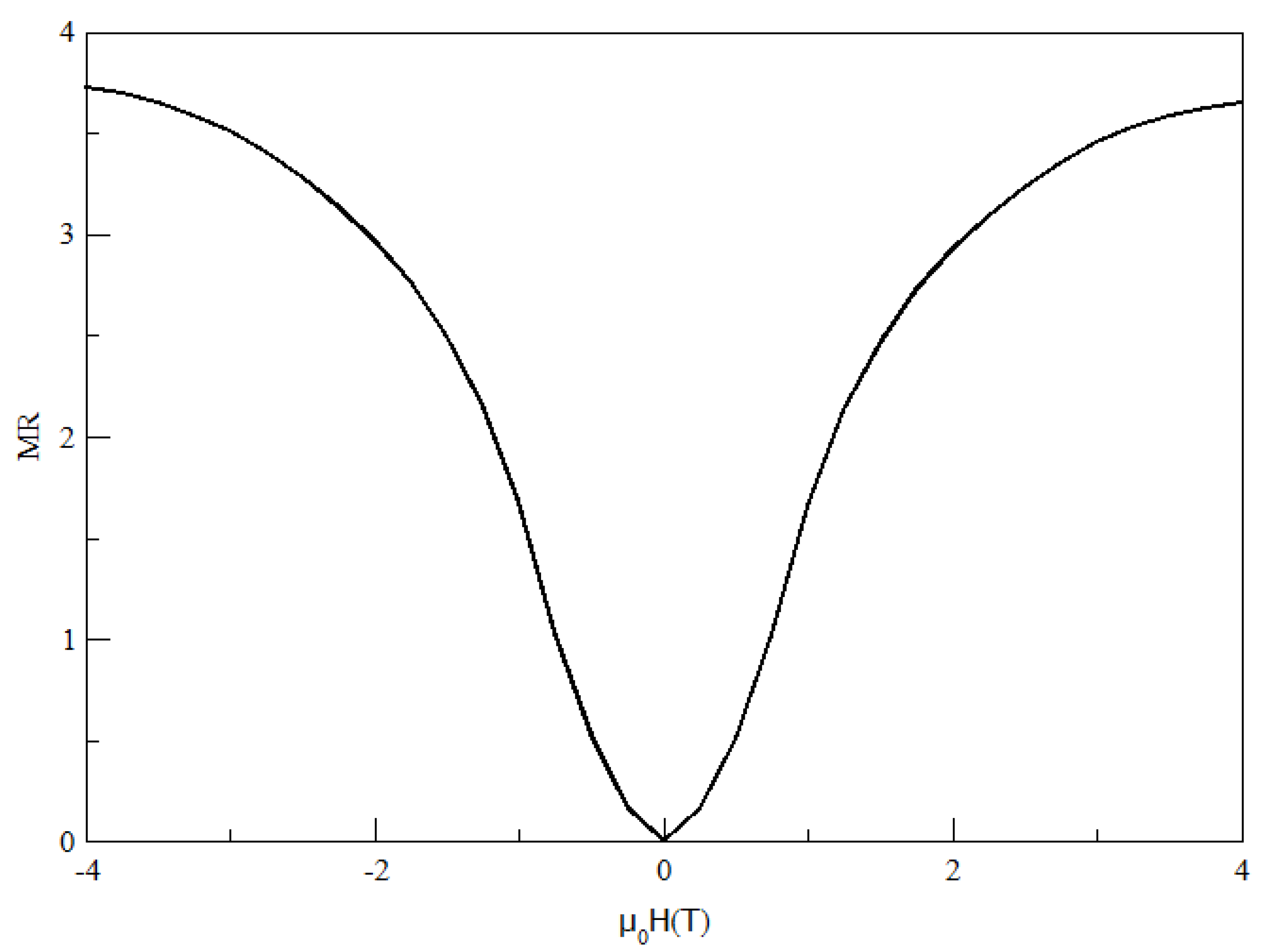
Electron transport in topological semimetals is strongly affected by the external magnetic field (B); hence, the measurement of magnetoresistance (MR) is commonly used as a signature indicator. The magnetic field dependence of both longitudinal and Hall resistivities were determined by applying the field perpendicular to the sample surface. The magnetoresistance for both transverse and longitudinal current transport were measured at a constant temperature of 1.8 K, where magnetoresistance (MR) is expressed as a change in resistivity due the field divided by the resistivity at zero field, i.e., . The field dependence of the MR for the longitudinal current transport is shown in Figure 4. At lower magnetic fields, there is a parabolic relationship between the applied magnetic field and the magnetoresistance. The parabolic profile of the plot of MR and the field is one of the characteristics of topological semimetals. This can be shown by using the following expression to determine resistivities with and without the field [26,27]:
where e is the electronic charge, the mobility, and n and p are the concentrations of electrons and holes. A common feature of all such systems is the existence of charge neutrality, where the concentrations and mobility of the positively and negatively charged particles are equal and the system is electrically neutral [27]. Then, in cases of charge neutrality or charge compensation, . However, at higher fields, the MR in these films seems to approach saturation, probably due to the presence of the second phase.
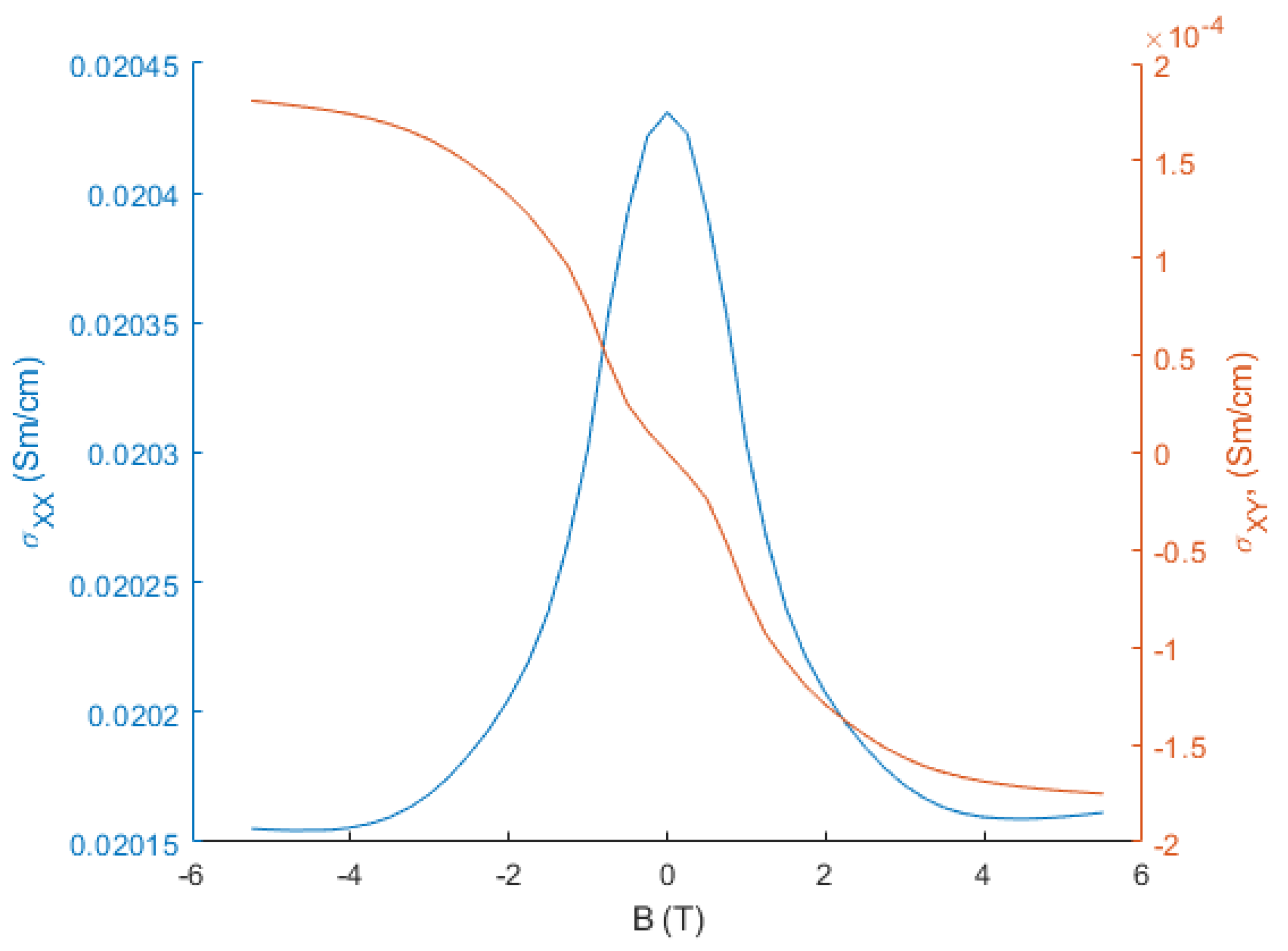
The Hall conductivity () and the longitudinal conductivity () at 1.8 K were extracted from their resistivities using the following relationships: and [9]. The experimental setup measured the magnitude of Hall voltage on the contacts; thus, for the Hall conductivity we first removed the contact resistance background and then inverted the sign of conductivity at the crossover (B = 0) field. The Hall and longitudinal conductivity are plotted against the magnetic field in Figure 5. In both cases, the largest change in the conductivities occurs at low fields where the magnetoresistance is low.
4. Conclusions
We have demonstrated the successful thin-film growth of MoP, a topological semimetal, using atomic layer deposition. The resistivity versus temperature measurement of the films shows a metallic behavior and the presence of a partial superconducting phase. With the introduction of a magnetic field perpendicular to the current paths, a parabolic relationship between the magnetic field and the resistivity is introduced. A DFT calculation of the crystal structure of MoP was performed to determine its lattice constants. These lattice parameters were in good agreement with those extracted from an XRD spectrum. Clearly, our growth conditions are not optimum since the films include a small amount of an unwanted phase. As we continue to refine the growth process, we are confident we can upgrade the quality of these films by optimizing conditions for a single- phase growth. Additionally, although the size of samples in our reactor is limited to 5 cm × 5 cm, the ALD technique is highly scalable, as evident by its use in the semiconductor fabs. The maturing of this technology will facilitate the widespread application of these novel materials in applications ranging from optics to spintronics, including interconnects for the next generation of semiconductor devices.
Supplementary Materials
The following supporting information can be downloaded at: https://www.mdpi.com/article/10.3390/applnano4010003/s1, Figure S1: SEM image of the grown films.
Author Contributions
All three authors contributed equally to this work; all three authors reviewed and revised the manuscript. All authors have read and agreed to the published version of the manuscript.
Funding
This research received no external funding.
Data Availability Statement
Data for the study are available upon reasonable request by contacting the corresponding author.
Acknowledgments
We wish to thank LaRosa’s group for providing access to some of the metrology tools.
Conflicts of Interest
The authors declare no conflict of interest.
References
- Chiu, C.K.; Teo, J.C.Y.; Schnyder, A.P.; Ryu, S. Classification of topological quantum matter with symmetries. Rev. Mod. Phys. 2016, 88, 035005. [Google Scholar] [CrossRef] [Green Version]
- Yan, B.; Felser, C. Topological Materials: Weyl Semimetals. Annu. Rev. Condens. Matter Phys. 2017, 8, 337–354. [Google Scholar] [CrossRef] [Green Version]
- Vafek, O.; Vishwanath, A. Dirac Fermions in Solids: From High-Tc Cuprates and Graphene to Topological Insulators and Weyl Semimetals. Annu. Rev. Condens. Matter Phys. 2014, 5, 83–112. [Google Scholar] [CrossRef] [Green Version]
- Lv, B.Q.; Feng, Z.L.; Xu, Q.N.; Gao, X.; Ma, J.Z.; Kong, L.Y.; Richard, P.; Huang, Y.B.; Strocov, V.N.; Fang, C.; et al. Observation of three-component fermions in the topological semimetal molybdenum phosphide. Nature 2017, 546, 627–631. [Google Scholar] [CrossRef] [Green Version]
- Han, H.J.; Kumar, S.; Ji, X.; Hart, J.L.; Jin, G.; Hynek, D.J.; Sam, Q.P.; Hasse, V.; Felser, C.; Cahill, D.G.; et al. Topological Metal MoP Nanowire for Interconnect. arXiv 2022, arXiv:2208.02784. [Google Scholar] [CrossRef]
- Weng, H.; Fang, C.; Fang, Z.; Bernevig, B.A.; Dai, X. Weyl Semimetal Phase in Noncentrosymmetric Transition-Metal Monophosphides. Phys. Rev. X 2015, 5, 011029. [Google Scholar] [CrossRef] [Green Version]
- Saleheen, A.I.U.; Chapai, R.; Xing, L.; Nepal, R.; Gong, D.; Gui, X.; Xie, W.; Young, D.P.; Plummer, E.W.; Jin, R. Evidence for topological semimetallicity in a chain-compound TaSe3. Npj Quantum Mater. 2020, 5, 53. [Google Scholar] [CrossRef]
- Zhang, Y.; Yin, Y.; Dubuis, G.; Butler, T.; Medhekar, N.V.; Granville, S. Berry curvature origin of the thickness-dependent anomalous Hall effect in a ferromagnetic Weyl semimetal. Npj Quantum Mater. 2021, 6, 17. [Google Scholar] [CrossRef]
- Kumar, N.; Sun, Y.; Nicklas, M.; Watzman, S.J.; Young, O.; Leermakers, I.; Hornung, J.; Klotz, J.; Gooth, J.; Manna, K.; et al. Extremely high conductivity observed in the triple point topological metal MoP. Nat. Commun. 2019, 10, 2475. [Google Scholar] [CrossRef] [Green Version]
- Gall, D.; Cha, J.J.; Chen, Z.; Han, H.J.; Hinkle, C.; Robinson, J.A.; Sundararaman, R.; Torsi, R. Materials for interconnects. MRS Bull. 2021, 46, 959–966. [Google Scholar] [CrossRef]
- Liu, P.; Williams, J.R.; Cha, J.J. Topological nanomaterials. Nat. Rev. Mater. 2019, 4, 479–496. [Google Scholar] [CrossRef]
- Gupta, T. The Copper Damascene Process and Chemical Mechanical Polishing. In Copper Interconnect Technology; Springer: New York, NY, USA, 2009; pp. 267–300. [Google Scholar] [CrossRef]
- Cha, J. Structure-Transport Properties of Topological Nanowires. Microsc. Microanal. 2021, 27, 920–921. [Google Scholar] [CrossRef]
- Cao, F.; Zheng, S.; Liang, J.; Li, Z.; Wei, B.; Ding, Y.; Wang, Z.; Zeng, M.; Xu, N.; Fu, L. Growth of 2D MoP single crystals on liquid metals by chemical vapor deposition. Sci. China Mater. 2021, 64, 1182–1188. [Google Scholar] [CrossRef]
- Hu, T.; Tai, G.; Wu, Z.; Wang, R.; Hou, C.; Sheng, L. Ultrathin molybdenum phosphide films as high-efficiency electrocatalysts for hydrogen evolution reaction. Mater. Res. Express 2018, 6, 016418. [Google Scholar] [CrossRef]
- Wang, W.; Qi, J.; Zhai, L.; Ma, C.; Ke, C.; Zhai, W.; Wu, Z.; Bao, K.; Yao, Y.; Li, S.; et al. Preparation of 2D Molybdenum Phosphide via Surface-Confined Atomic Substitution. Adv. Mater. 2022, 34, 2203220. [Google Scholar] [CrossRef] [PubMed]
- Han, H.J.; Hynek, D.; Wu, Z.; Wang, L.; Liu, P.; Pondick, J.V.; Yazdani, S.; Woods, J.M.; Yarali, M.; Xie, Y.; et al. Synthesis and resistivity of topological metal MoP nanostructures. APL Mater. 2020, 8, 011103. [Google Scholar] [CrossRef]
- Suntola, T. Atomic layer epitaxy. Mater. Sci. Rep. 1989, 4, 261–312. [Google Scholar] [CrossRef]
- Plachinda, P.; Hopkins, M.; Rouvimov, S.; Solanki, R. Topological Insulator Bi2Se3 Films on Silicon Substrates. J. Electron. Mater. 2020, 49, 2191–2196. [Google Scholar] [CrossRef]
- Saiki, K.; Ueno, K.; Shimada, T.; Koma, A. Application of Van der Waals epitaxy to highly heterogeneous systems. J. Cryst. Growth 1989, 95, 603–606. [Google Scholar] [CrossRef]
- Perdew, J.P.; Ruzsinszky, A.; Csonka, G.I.; Vydrov, O.A.; Scuseria, G.E.; Constantin, L.A.; Zhou, X.; Burke, K. Restoring the Density-Gradient Expansion for Exchange in Solids and Surfaces. Phys. Rev. Lett. 2008, 100, 136406. [Google Scholar] [CrossRef] [Green Version]
- Li, W.; Dhandapani, B.; Oyama, S.T. Molybdenum Phosphide: A Novel Catalyst for Hydrodenitrogenation. Chem. Lett. 1998, 27, 207–208. [Google Scholar] [CrossRef]
- Phillips, D.C.; Sawhill, S.J.; Self, R.; Bussell, M.E. Synthesis, Characterization, and Hydrodesulfurization Properties of Silica-Supported Molybdenum Phosphide Catalysts. J. Catal. 2002, 207, 266–273. [Google Scholar] [CrossRef]
- Shirotani, I.; Kaneko, I.; Takaya, M.; Sekine, C.; Yagi, T. Superconductivity of molybdenum phosphides prepared at high pressure. Phys. B Condens. Matter 2000, 281–282, 1024–1025. [Google Scholar] [CrossRef]
- Zatsepin, D.A.; Green, R.J.; Hunt, A.; Kurmaev, E.Z.; Gavrilov, N.V.; Moewes, A. Structural ordering in a silica glass matrix under Mn ion implantation. J. Phys. Condens. Matter 2012, 24, 185402. [Google Scholar] [CrossRef]
- Kumar, N.; Guin, S.N.; Manna, K.; Shekhar, C.; Felser, C. Topological Quantum Materials from the Viewpoint of Chemistry. Chem. Rev. 2021, 121, 2780–2815. [Google Scholar] [CrossRef]
- Alekseev, P.S.; Dmitriev, A.P.; Gornyi, I.V.; Kachorovskii, V.Y.; Narozhny, B.N.; Schütt, M.; Titov, M. Magnetoresistance of compensated semimetals in confined geometries. Phys. Rev. B 2017, 95, 165410. [Google Scholar] [CrossRef] [Green Version]
Figure 1.
Structure of a monolayer of hexagonal MoP produced by DFT simulation.

Figure 2.
Grazing incidence XRD of MoP film.

Figure 3.
Resistivity versus temperature plot showing a metallic behavior of the MoP film.

Figure 4.
Relationship between the applied perpendicular magnetic field and the magnetoresistance MR.
Figure 4.
Relationship between the applied perpendicular magnetic field and the magnetoresistance MR.

Figure 5.
Longitudinal and Hall conductivities as a function of the magnetic field at 1.8 K.

Disclaimer/Publisher’s Note: The statements, opinions and data contained in all publications are solely those of the individual author(s) and contributor(s) and not of MDPI and/or the editor(s). MDPI and/or the editor(s) disclaim responsibility for any injury to people or property resulting from any ideas, methods, instructions or products referred to in the content. |
© 2023 by the authors. Licensee MDPI, Basel, Switzerland. This article is an open access article distributed under the terms and conditions of the Creative Commons Attribution (CC BY) license (https://creativecommons.org/licenses/by/4.0/).
Share and Cite
MDPI and ACS Style
Browning, R.; Plachinda, P.; Solanki, R. Thin Film Deposition of MoP, a Topological Semimetal. Appl. Nano 2023, 4, 38-44. https://doi.org/10.3390/applnano4010003
AMA Style
Browning R, Plachinda P, Solanki R. Thin Film Deposition of MoP, a Topological Semimetal. Applied Nano. 2023; 4(1):38-44. https://doi.org/10.3390/applnano4010003
Chicago/Turabian StyleBrowning, Robert, Paul Plachinda, and Raj Solanki. 2023. "Thin Film Deposition of MoP, a Topological Semimetal" Applied Nano 4, no. 1: 38-44. https://doi.org/10.3390/applnano4010003