
Tunability of the Optical Properties of Transition-Metal-Based Structural Phase Change Materials
by
 ,
,
Sheheera Irfan
1,
Yasir A. Haleem
1,*,
Muhammad Imran Irshad
1,
Muhammad Farooq Saleem
2 ,
,
Muhammad Arshad
3 and
Muhammad Habib
4 1
Institute of Physics, Khwaja Fareed University of Engineering and Information Technology, Rahim Yar Khan 64200, Pakistan
2
GBA Branch of Aerospace Information Research Institute, Chinese Academy of Sciences, Guangzhou 510700, China
3
Nano Sciences and Technology Department, National Centre for Physics, Quaid-e-Azam University, Islamabad 45320, Pakistan
4
Department of Physics, COMSATS University of Islamabad, Lahore 45550, Pakistan
*
Author to whom correspondence should be addressed.
Optics 2023, 4(2), 351-363; https://doi.org/10.3390/opt4020026
Submission received: 22 February 2023
/
Revised: 13 April 2023
/
Accepted: 8 May 2023
/
Published: 24 May 2023
(This article belongs to the Special Issue Opto-Thermo-Mechanical Interactions in Nano-Objects and Metasurfaces)
Abstract
:Phase transitions are an intriguing yet poorly understood aspect of transition-metal-based materials; these phase transitions can result in changes to the refractive index, absorption coefficient, and other optical properties of the materials. Transition-metal-based materials exist in a variety of crystalline phases and also have metallic, semi-metallic, and semi-conducting characteristics. In this review, we demonstrate that alloyed W- and Mo-based dichalcogenides enable phase transitions in structures, with phase transition temperatures that are tunable across a wide range using various alloy models and modern DFT-based calculations. We also analyze the tuning the optical bandgap of the metal oxide nanoparticles through doping of the transition metal in a manner that is suitable for optical switching and thermal imaging. After the introduction and a brief illustration of the structures and their exceptional properties, we discuss synthetic methodologies and their application as part of important strategies toward the enhanced performance of transition-metal-based dichalcogenides and oxides. In the end, our conclusion highlights the prospects of 2D materials as phase transition materials due to their advantages in terms of scalability and adaptability.
1. Introduction
A number of decades ago, researchers from all over the world began focusing on a broad category of two-dimensional (2D) transition materials that presented distinct challenges to our understanding of materials chemistry and physics. Two-dimensional nanomaterials are a broad category of crystals that range from complex compounds to elemental allotropes [1]. Transition metal dichalcogenides and oxides are the most prominent groups of 2D crystalline compounds [2]. Investigations of 2D materials have been stimulated by their intriguing optical, catalytic, and electronic characteristics. These characteristics can be tuned not only by functionalization, composition, and size but also by the phase and structure of the crystal. Two-dimensional materials often exhibit, for a given material, crystal phases with substantially diverse optical and electronic properties, a diversity that allows for unique phenomena [3]. As a result of their expectational characteristics and lower energetic switching costs, transition-metal-based dichalcogenides with the ability to switch between semi-metallic, metallic, and semi-conducting phases are of great interest for next-generation electronics, including those incorporating phase change memory and its corresponding applications [4].
Most research has focused on transition-metal-based dichalcogenides with semi-metallic distorted octahedral coordinate 1T′ phases, metallic octahedral coordinate 1T phases, and semi-conducting trigonal coordinate 2H phases [5]. Phase change and phase control have been observed in TMDs via alkali metal intercalations, electrostatic gating [6], alloying [7], joule heating [8], and thermal treatment [9].
Among binary transition metal dichalcogenides, MoTe2 has the smallest difference in energy between the 1T´ semi-metallic and the 2H semi-conducting phase, with the ability to further lower the energy gap by alloying with tungsten [10]. Furthermore, computational studies on MoTe2 monolayers have revealed that the minimal energy gap between the 1T′ and 2H phases allows for charging by electrostatic gating to achieve a phase transition [11]. As a result of its reversibility, energy efficiency, and speed, electrostatic phase changes via field-induced charge doping are a more desirable switching mechanism for advancing devices.
Wang et al. reported a reversible phase transition in the monolayer of MoTe2 and the first use of a gated ionic liquid at 220 K in a vacuum, confirming density functional theory (DFT) research [6]. Furthermore, we have expanded upon prior findings to demonstrate a phase transition in the range of MoTe2 thickness to bulk-like thickness (73 nm) from monolayers. This was achieved by the use of ionic liquid gating with N, N-diethyl-N-(2-methoxyethyl)-N-methylammonium bis (trifluoromethyl sulphonyl)-imide (DEME-TFSI) in air under ambient conditions. They showed convincing evidence of a partly irreversible 2H–1T′ transition using Raman spectroscopy, with the emergence of two different 1T′ Raman modes that are also widely detected in pure 1T′ but have not previously been reported in 1T′ MoTe2 generated by a phase change from the 2H phase [9]. Second, they showed how the formation of Te vacancies influences the phase transition not only electrostatically, but also mediate electrochemically during gating process. [11]. Te vacancies have also been demonstrated to decrease the energy gap between the phases of 2H and 1T′, as well as the doped density of charge required for switching MoTe2 flakes thicker than monolayers [12,13,14]. Furthermore, in this study, the polarization-resolved Raman spectroscopy results show that the 1T′ phase forms in polycrystalline materials, with domains produced heterogeneously and with a distinct 2H phase in crystallographic directions. These findings show that MoTe2 can change phase under a variety of practical conditions and thus indicate that MoTe2 has the potential for phase change memory. This also implies that targeted vacancy formation or the flake thickness might be an effective tuning parameter for phase change memory.
To precisely tune the characteristics of any material, one must first understand its atomic structure. When no crystals are accessible for a single crystalline structural analysis, the structure of a crystal may typically be solved using an X-ray powder diffraction pattern. Furthermore, if the quality of the experimental data is minimal or the structure is incredibly unique, predicting the entire structure from powder data becomes extremely challenging [15]. Multiple computational techniques have been proposed to predict the crystal structure, leading to improvements in the structural determination of novel materials as well as material design processes [16,17,18,19]. Although there have been some significant advancements, crystal structure modelling has long been known to be among the most difficult problems in material science [20,21].
Transition-metal-based oxides are an important family of crystal forming and phase change materials. Transition metal oxides are important in a vast range of applications, from electronics to catalysis. It is widely noted that GGA [22] functionals, including PBE, cannot accurately represent the structure of electronic systems such as correlated oxides of transition metals [23].
The reason behind this is GGAs self-interaction inefficiency [24], which results in electron over-delocalization on the 3d orbital of TMs as well as the 2p orbital of oxygen. As a result, even an intrinsic electronic structure becomes inaccurate [25]. The dilemma of de-localization of the orbitals in 3D can be solved by the Hubbard parameter, which localizes the electrons on the atoms of a transition metal, but it fails to solve the dilemma of oxygen 2p orbital electron over-delocalization [26]. Recent work has conclusively illustrated that functionals of hybrids exclusively localize the density into the 2p orbitals, while DFT + U does not always do so [27]. Consequently, GGA + U underestimates the bandgap of transition metal monoxides [28]. Furthermore, if the aim is to estimate unique crystal structures, it is unclear whether a specific value of U should be employed if the material is completely novel [29]. Problems with the correction of U could be handled by using hybrid and exact exchange DFT [30], which increases the localization on oxygen and the TM atom and also has an influence on the sites of energy levels of transition metal d orbital and the p orbitals of oxygen. Among the fundamental differences between hybrid functionals and the GGA + U method is that the quantity of the exact exchange in hybrid DFT is not set for each material [31]. Additionally, hybrid functionals with twenty percent exact exchange have been shown to accurately represent the optical and electronic characteristics of transition metal oxides [32]. In the present work, we demonstrate that alloyed W- and Mo-based dichalcogenides enable phase transitions in the structure and that phase transition temperatures are tunable across a wide range using various alloy models and up to date DFT-based calculations. They analyze the temperature–composition phase diagram of alloys comprising pure Mo- and W-based TMDs and compare them to corresponding bulk material investigations. They also analyzes the optical bandgap of metal oxide nanoparticles, which can be tuned by doping with a transition metal, which could be suitable for different applications.
2. Phase Change
We analyze here the phase change between the semi-metallic 1T′ phase and the semi-conducting phases of MoTe2 flakes. Their thickness ranges from monolayers to a few layers, which, in terms of their electrical and spectroscopic characteristics, means they are regarded as bulk-like, though they remain optically thin [6]. Gated DEME-TFSI zeolite was used to infuse charge into MoTe2 as it has been proven to produce a charge density substantial enough to trigger a phase shift. The 1T′ and 2H phases show distinct crystal structures with different phonon modes. Raman spectroscopy was used to examine the results of the phase change.
2.1. Phase Change (Bulk-Like MoTe2)
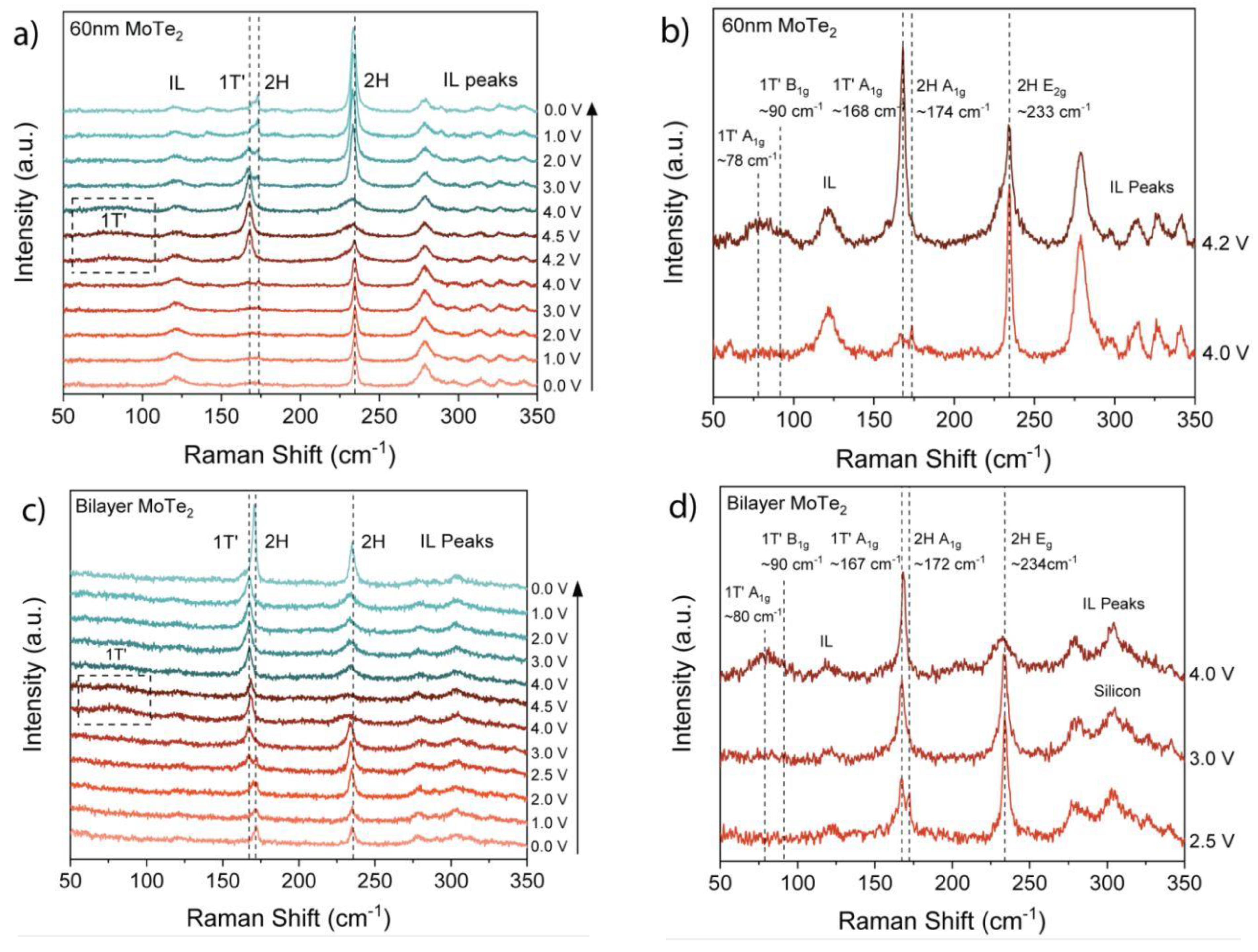
By Raman spectroscopy, the gating cycle of MoTe2 was obtained as shown in Figure 1a,b. A distinctive vibration mode is observed out of the plane for 2H at 173 cm−1, while it is observed at 234 per cm in the plane. The A1g peak has a low intensity, which is a property of the bulk as the vibrations are reduced by the interactions of multiple layers. The peak at 120 cm−1 is broader. The peaks that appear in the range of 270 to 350 cm−1 are due to the anion TFSI as well as the cation DEME in zeolite [33]. No significant peaks are observed when the voltage is increased by four electron volts. The voltage required for a phase change is 4.0 V, as shown by the initial development of a small 1T′ A1g peak at 168 cm−1 s. The Raman peaks of 1T′ are comparable with the reported values and confirm the phase change. This voltage initiates the nucleation of 1T′ domains in the flakes of 2H [34]. At 4.2 V, there is a significant rise in the intensity of the 1T′ A1g peak, which is accompanied by a reduction in intensity and a widening of the 2H E2g peak.
Simultaneously, it was observed that the formation of peaks occurs at 78 as well as 90 per cm, which also indicate the 1T′ modes of A1g and B1g. These peaks have not been identified in 2H to 1T′ MoTe2 phase transition observations, yet they have frequently been described in the DFT and CVD (chemical vapor deposition) growth literature as substantial 1T′ peaks [35]. Raman modes are inversely proportional to the phonon lifetime, with wider linewidths indicating a rapid decay of the phonon, which is attributable to an increase in defects.
Multiple impacts are noticed when the charge is removed. The 78 and 90 cm−1 peaks vanish at 3 V, confirming that they are caused by gate-induced phase transitions. The 168 1T′ peak, on the other hand, is still present but weakens. This reduction in the intensity of both 1T′ and 2H E2g peaks correlate with a rise in the intensity of the A1g and 2H E2g peaks above their initial intensity [36,37]. At this point, the increase in intensity is not fully understood, although it is more likely due to multiple beams of reflection and interference which is a reliable in layered 2D materials.
Similarly, amplification of the Raman peaks were observed while adjusting the thickness of the substrate beneath graphene, as well as during graphene and MoS2 intercalation. The 1T′ MoTe2 phase transitions to the 2H phase at 1 V, with a peak corresponding to the 2H A1g phase observed at 172 cm−1. In short, the process of the phase change in thick flakes tends to be slightly reversible.
2.2. Phase Change (Bilayer MoTe2)
A similar phase change phenomenon also appears in bilayer MoTe2 as it does in bulk-like MoTe2. The peaks of the 2H E2g and 2H A1g phases begin with relatively equal intensities, as is typical for bilayer MoTe2. The peak 2H E2g voltage does not fall until it reaches 4 V. When the voltage is 4V, the intensity drops significantly, and wide peaks of 1T´ are observed at 80 cm−1 and 90 cm−1, as shown in the below Figure 1c,d. When the flake is discharged, it only reverses to the phase of 2H at 0 V, demonstrating that somehow a significant kinetic barrier generates hysteresis, as described earlier. The intensities of the 2H peaks are higher at 0 V before gating, which we equate to the phenomenon of optical interference. We additionally see that the amplitude of the 2H E2g peak is less than the 2H A1g peak, which is consistent with monolayer MoTe2 and signifies the transition from bilayer to monolayer MoTe2, although we are unable to ascertain at which voltage the thinning originated. Despite being thin, the phase change is not the consequence of irreversible heating pyrolysis, since change is reversible to the 2H phase after cycling.
2.3. Phase Change Mechanism
The 2H E2g peak does not ever completely vanish, as in the bilayer and bulk-like investigations outlined in the previous section, demonstrating the presence of 1T′ and 2H phases. The existence of these peaks indicate two possibilities. Primarily, the phase change happens on the top, or perhaps the upper few layers, and the characteristics of the 2H Raman spectrum come from the sublayer [38]. However, even in the uppermost layers, the phase transition is incomplete, and the Raman spectra indicate domains at the interface of 1T′ and 2H as well. We suggest that the reported result is a confluence of both phenomena [39].
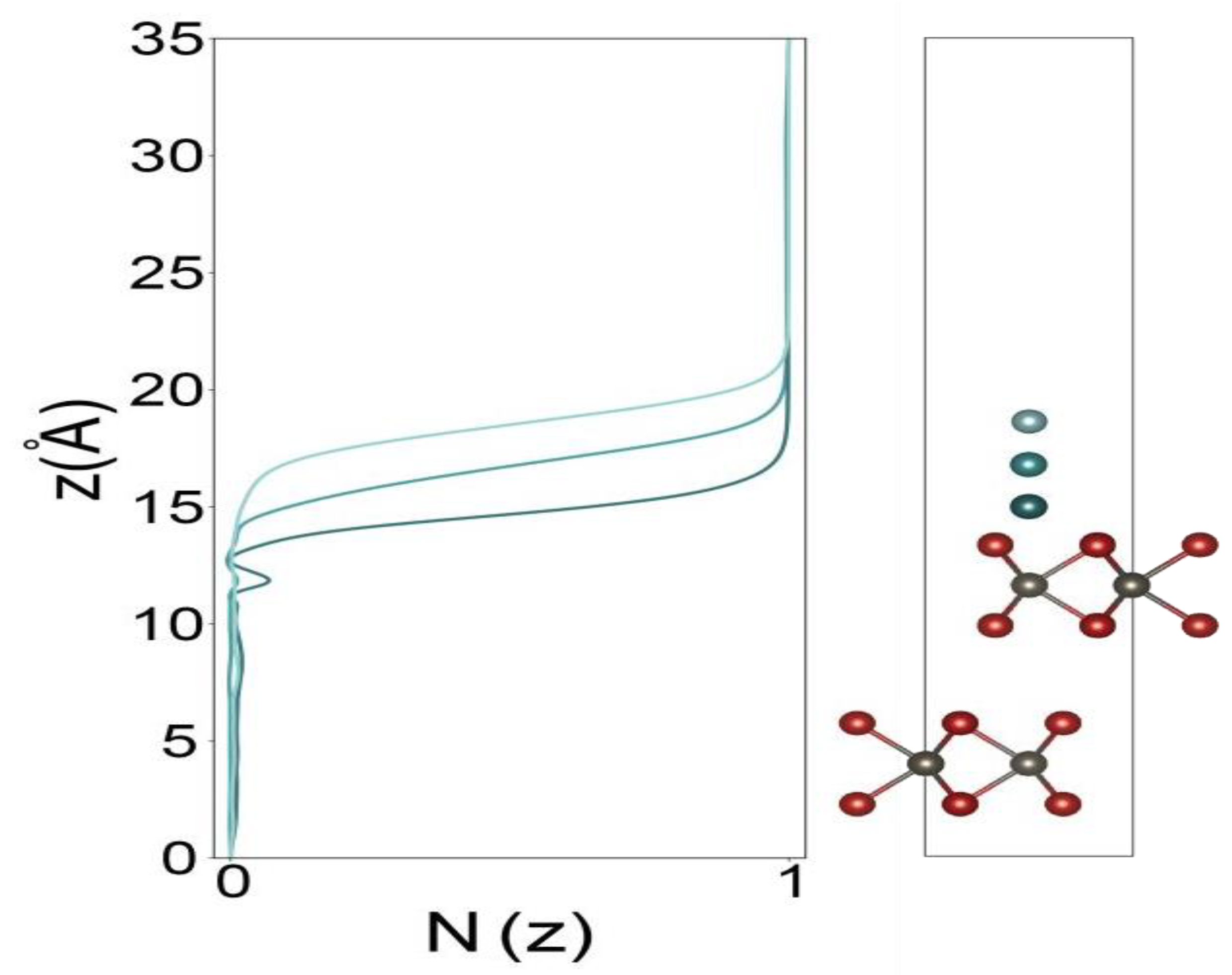
We use density functional theory (DFT) computations on a structure that consists of a lithium atom resting on top of a 2H MoTe2 bilayer. To evaluate the doping of the bilayer by electrons, the lithium atom is used as a substitute for the ionic liquid [40,41,42]. The charge amount that passes from an atom of lithium to the bottom layer is a significant factor [43]. For these estimations, we computed the relative charge of the unpaired electron arising from the lithium atoms, N(z), at three distinct positions in the unit cell above the z bilayer, as represented in the below Figure 2.
In the above equation [44], the first term represents the Li + bilayer charge density, while the second term represents the bilayer charge density. We demonstrate that there is no noticeable charge density beyond the initial layer, despite the position of the Li atom with regard to the surface.
According to the hypothesis, Te vacancies induced by the gating mechanism enable the mobility of Te atoms, influencing the transfer of charge across layers. Moreover, we propose that the 1T’ A1g and 1T’ B1g modes suggest a few-layer phase transition, wherein additional layers of 1T’ enhance the Raman peaks and allow them to be observed. This proposition is based on two observational data points: first, the 1T′ mode peaks at 80 and 90 cm−1 do not always disappear and appear simultaneously with the primary peak, implying a layer-by-layer phase change process. Furthermore, the peaks arise or vanish simultaneously with the decrease or increase in the above-mentioned peaks, demonstrating that the loss of the pure 2H signal is correlated to the observation of the peaks of 1T′. We may expect a significant 2H E2g signal from the base of pure 2H layers, which are not altered in the bulk-like scenario. At 3 V, the 80 and 90 cm−1 1T′ peaks vanish, the 168 cm−1 1T′ peak is maintained, and the 2H E2g peak intensifies, indicating that the subsurface layers of 1T′ have reverted to 2H while only the topmost layer of 1T′ remained. Such observations are also valid in the case of a bilayer, although the uncertainty of how the thinning begins makes such a prediction difficult to prove.
Interestingly, when we characterize the spectrum as a bilayer or a monolayer owing to thinning in the bilayer experiment at 4 V, the 2H E2g peak does not disappear entirely [44]. This analysis reveals that the phase transition to 1T′ from 2H is not complete, with patches of 2H MoTe2 existing in the layer. Therefore, it is assumed that the phase shift arises in the topmost layers, indicating that the lateral distribution of the change in phase is not significant. We further investigate the feasibility of the hypothesis that the phase change is driven by the intercalation of DEME cations in flakes of MoTe2. However, we observed no indications of intercalation when utilizing ex situ XRD [45]. Additionally, when intercalation increases the local thickness of the flake and varies the length of the optical path for interference, the hue of the flake varies from the edge to the center. In these trials, however, the color change took place simultaneously throughout the entire flake surface.
3. Synthesizing Strategy of Material
A sustainable synthesis of nanoscale 2D TMDCs exhibiting homogeneous characteristics is crucial for applying their unique optical and electronic features. Here, we discuss the various approaches for top-down exfoliation of bulk materials and for bottom-up syntheses and evaluate their respective merits. Designing strategies for synthesizing vast areas and homogenous layers is crucial for applications such as ultrathin electronic gadget production and extensible, translucent optoelectronics. As proven earlier for graphene, the development of ultra-thin synthesis techniques utilizing CVD (chemical vapor deposition) on metallic substrates and epitaxial growth on SiC substrates has enabled large yields [46] in the fabrication of devices [47,48,49]. Furthermore, certain CVD techniques for synthesizing nanoscale MoS2 films onto insulating substrates have been proposed [50,51]. Several CVD-related approaches are outlined below. In many of these procedures, the resultant MoS2 film thickness is influenced by the concentrations or thicknesses of the starting precursors; however, precise control of the number of layers throughout a broad area is yet to be accomplished. CVD synthesis of MoS2 has also been observed, with recently CVD-grown graphene on Cu foil serving as a substrate pattern, yielding single-crystal layers of MoS2 several microns thick. Such CVD investigations are still preliminary; nevertheless, they show promise for future research that will result in the development of materials other than MoS2. A hydrothermal synthesis has also been used to chemically synthesize MoS2 [52] and MoSe2 [53]. Matte et al., recently outlined numerous ways for synthesizing WS2, MoS2, WSe2, and MoSe2, as well as detailing the reactions of molybdic and tungstic acid with thiourea at high temperatures to provide an appropriately layered TMDC material [54,55]. Such processes produce moderately better materials, with typical flake sizes ranging from a few nanometers to a few microns in size, although the flakes thicknesses have not been proven to be monolayers.
Nanoscale layers of TMDCs can be peeled from their parental crystalline structure using adhesive tape adhered to surfaces [56,57], then optically characterized utilizing light interference approaches, which has been described for graphene [58]. This approach could also be used to mechanically exfoliate layered materials such as BN, dichalcogenides, and oxide nanosheets into single sheets [59]. Mechanical cleavage yields single-crystal flakes of exceptional purity and uniformity, which are appropriate for primary characterization and device fabrication [60].
This approach, however, is not scalable [61] and does not allow for the systematic control of flake thickness or size [62]. A concentrated laser spot has reportedly been applied to minimize the MoS2 monolayer thickness by thermal ablation at micro scale resolution, but the requirement for laser raster scanning makes it challenging for scale up [63]. Liquid phase TMDC compositions are extremely promising for producing huge numbers of exfoliated nanosheets [64]. Other advancements include composites and hybrids formed by reliable mixed dispersions of various materials, as well as thin coatings and films developed by filtering, spray painting, and medical blading [65].
Even though solution-based graphene has been utilized to achieve higher frequency flexible electronics with a current gain cut-off frequency of 2.2 GHz, we anticipate that solution-based TMDCs will still have analogous promising aspects for the fabrication of flexible electronics and composites. The diffusion of TMDs anions enables liquid exfoliation of such layers [66]. Morrison and co-workers developed the intercalation approach in the 1970s and subsequently developed exfoliation to thin layers in the 1980s, and both technologies are gaining traction again [67].
The conventional process involves submerging bulk TMDC powder into a solution of a lithium-containing substance, such as n-butyllithium, for more than a day to allow the lithium ions to intercalate, followed by exposing the intercalated substance to water. The liquid between the layers vigorously reacts with the lithium to produce H2 gas, which rapidly separates the layers. Lithium-based intercalation and exfoliation yielded solution-phase flakes of MoS2. Even though such chemical exfoliation approaches provide substantial amounts of submicron monolayers, the resultant exfoliated material varies structurally and electrically from the composite [68]. Regarding MoS2, the approach modifies the exfoliated nanosheets’ electronic structure from metallic to semiconducting, as well as altering the Mo atom coordinates from trigonal crystalline (2H-MoS2) to octahedral (1T-MoS2). Annealing at 300 °C can trigger a phase transition from 2H-MoS2 to 1T-MoS2, regaining Mo atom coordination as well as the pristine material’s semiconducting bandgap, as demonstrated by the re-emergence of bandgap photoluminescence [69]. For nanoelectronic and optoelectronic devices, effective control over the nanosheet thickness and size is likely to be required. By comparison with graphene, novel layer-controlled chemistries or post-synthesis flake sorting by film thickness and lateral size might also provide an alternative.
The electronic structure of semiconducting TMDs is represented by MX2, where M = W or Mo and X = Se, Te, or S. All combinations have hexagonal symmetry and are thus part of the P63/mmc group. The strained and unstrained electronic structures of TMD monolayers were estimated via DFT-based methodologies [70] as embodied in the Vienna ab initio simulation software (VASP). Electron–ion interactions were handled using PAW (projector-augmented wave) potentials, whereas electron exchange–correlation interactions were handled using Perdew Burke Ernzerhof’s GGA (generalized gradient approximation). A conjugate gradient approach was used to optimize the atomic coordinates and lattice vectors to achieve the unstrained configuration [71]. To form the strained cell in the case of strained geometries, the lattice vectors were modulated at a constant rate and atoms were permitted to relax. Atomic relaxation was carried out until the interatomic forces fell below 0.01 eV, which was determined to be sufficient for obtaining relaxed parameters. During relaxation computations, a k-point sample of 35 × 35 × 1 was employed, and a denser mesh of 45 × 45 × 1 was considered after relaxation to yield densities of states and charge densities. For all computations, a plane wave cut-off of 400 eV was employed, and a vacuum of about six layers was provided to preclude interaction between periodic images of slabs in the z-direction, as shown in Figure 3.
To examine various configurations of strained cells, the strain was applied to all TMDs in a symmetrical as well as an asymmetrical manner. Mainly, five different types of strain distributions were studied, which included (i) expansion in the x-direction (xx), (ii) expansion in y-direction (yy), (iii) homogeneous biaxial expansion in x- and y-directions (xx + yy), (iv) expansion in the x-direction and compression in the y-direction (xx + yy), and (v) compression in the x-direction and expansion in the y-direction (yy − xx) with the same magnitude of strain.
The first three strain profiles correspond to tensile strain, while the latter two are examples of pure shear strain. Except for the pure shear strain where the system is expanded in the x-direction and compressed in the y-direction, all types of strain profiles lead to an increase in the lattice parameter as compared to its optimized value in the below Table 1 [72].
Figure 3.
An iso-surface plot of the charge density (n) of chalcogenide atoms of monolayer MoS2 (top), MoSe2 (middle), and MoTe2 (bottom) when they are expanded along the x-/y-direction and compressed along the y-/x-direction (xxyy/yyxx) by 2%, 6%, and 10%. The isosurface value was taken as 0.05 e/Å3 (reprinted with the permission of ACS Nano).

4. Applications
Two significant application categories include electroluminescence and photoluminescence. Photons are radiated in electroluminescence in response to an electrical stimulus; this feature is important in optoelectronic devices, which include LEDs and laser diodes. In photoluminescence, a photon is absorbed and afterwards re-radiated, occasionally with a different energy. The recombination of holes and electrons in direct bandgap semiconductors emits photons substantially more accurately than in indirect bandgap semiconductors. Graphene lacks a bandgap and needs chemical treatment to generate new bandgaps that optically luminesce; however, monolayer semiconductor materials such as TMDCs have direct bandgaps, making them suitable candidates for the active light-emitting layer in prospective flexible optoelectronics [75,76]. Electroluminescence from MoS2 exfoliated by lithium intercalation and integrated into a nanocomposite polymer matrix is a good example of electroluminescence in TMDCs. Photoluminescence is observed in monolayer MoS2, which has a direct bandgap, and the quantum yield of monolayer MoS2 photoluminescence is substantially greater than that of bilayer and bulk MoS2. Nevertheless, as previously stated, the photoluminescent quantum yield measured in MoS2 is significantly lower than what would be expected for a direct gap semiconductor, but much work would be required to comprehend the photoluminescence emission and quenching processes before viable optoelectronic devices can be fabricated.
Thermal and optoelectronic devices employ electronic charge and spin to transmit signals, respectively. Another useful attribute of charge carriers is the valley index, which corresponds to the confinement of holes or electrons in distinct conduction band minima as well as valence band maxima with the same energies but in distinct positions in momentum space, possibly leading to a ‘valleytronics’ device [77]. Materials that exhibit high spin splitting, which can be caused by numerous factors that drive the system out of equilibrium or by phase transitions, allow for the maintenance of spin-polarized carrier populations and are required for device fabrication. As a result of the lack of inversion symmetry and the significant spin–orbit coupling, spinning and valley physics are also coupled. Three different groups have established valley confinement in monolayer MoS2, where the carrier populations in various valleys can be regulated by optically stimulating the samples with circularly polarized light. Such an advancement might pave the way to a new domain of valleytronics devices. The above spin, orbit, and valley features are particular to TMDCs and may lead to new unanticipated applications.
5. Conclusions
We have outlined the rapid advancement of transition-metal-based chalcogenides and oxides in the last decade to contribute as a reference for future researchers in this area. We described the idea of a 2H to 1T′ phase transition in MoTe2 flakes after ionic liquid gating under ambient conditions, with the thickness of the flake ranging from bulk MoTe2 to monolayer MoTe2. We demonstrate that the phase transition is temporary by electrostatic and also electrochemical doping mediated by the creation of Te vacancies, which was substantiated by Te metal formation. Since not all the 2H in a specific layer is changed to 1T′, the process produces a mixture of phases, with the transition possibly occurring outside of the initial layer. Furthermore, the 1T′ domains are nucleated by variable crystal orientations, resulting in a loss of the 1T′ Raman spectrum’s polarization dependency. This report also signifies the importance of an electrochemical and an electrostatic mechanism of switching, as well as of the implications of Te defects and the need for a thorough understanding of them. Pre-treating MoTe2 devices by annealing or electrochemical destabilization to create Te defects may be a means to adjust the transition voltage into the desired range for phase change memory applications. Generally, there are many promising advantages of the tunability of transition-metal-based dichalcogenides. However, much more research is still needed to boost further advancements.
Author Contributions
Conceptualization and supervision, Y.A.H.; write up of manuscript and extraction of review content, S.I.; revision and formal analysis, M.F.S.; evaluation and assessment, M.I.I.; visualization and validation, M.A.; Review and editing, M.H. All authors have read and agreed to the published version of the manuscript.
Funding
This research received no external funding.
Institutional Review Board Statement
Not applicable.
Informed Consent Statement
Not applicable.
Data Availability Statement
Data analyzed in this study were a re-analysis of existing data, reuses with the permissions (ACS nano).
Conflicts of Interest
The authors declare no conflict of interest.
References
- Butler, S.Z.; Hollen, S.M.; Cao, L.; Cui, Y.; Gupta, J.A.; Gutiérrez, H.R.; Heinz, T.F.; Hong, S.S.; Huang, J.; Ismach, A.F. Progress, challenges, and opportunities in two-dimensional materials beyond graphene. ACS Nano 2013, 7, 2898–2926. [Google Scholar] [CrossRef] [PubMed]
- Manzeli, S.; Ovchinnikov, D.; Pasquier, D.; Yazyev, O.V.; Kis, A. 2D transition metal dichalcogenides. Nat. Rev. Mater. 2017, 2, 17033. [Google Scholar] [CrossRef]
- Rehn, D.A.; Li, Y.; Reed, E.J. Refrigeration in 2D: Electrostaticaloric effect in monolayer materials. Phys. Rev. Mater. 2018, 2, 114004. [Google Scholar] [CrossRef]
- Nyshadham, C.; Rupp, M.; Bekker, B.; Shapeev, A.V.; Mueller, T.; Rosenbrock, C.W.; Csányi, G.; Wingate, D.W.; Hart, G.L. Machine-learned multi-system surrogate models for materials prediction. NPJ Comput. Mater. 2019, 5, 51. [Google Scholar] [CrossRef]
- Duerloo, K.-A.N.; Li, Y.; Reed, E.J. Structural phase transitions in two-dimensional Mo-and W-dichalcogenide monolayers. Nat. Commun. 2014, 5, 4214. [Google Scholar] [CrossRef]
- Wang, Y.; Xiao, J.; Zhu, H.; Li, Y.; Alsaid, Y.; Fong, K.Y.; Zhou, Y.; Wang, S.; Shi, W.; Wang, Y. Structural phase transition in monolayer MoTe2 driven by electrostatic doping. Nature 2017, 550, 487–491. [Google Scholar] [CrossRef]
- Oliver, S.M.; Beams, R.; Krylyuk, S.; Kalish, I.; Singh, A.K.; Bruma, A.; Tavazza, F.; Joshi, J.; Stone, I.R.; Stranick, S.J. The structural phases and vibrational properties of Mo1−xWxTe2 alloys. 2D Mater. 2017, 4, 045008. [Google Scholar] [CrossRef]
- Zhang, F.; Zhang, H.; Krylyuk, S.; Milligan, C.A.; Zhu, Y.; Zemlyanov, D.Y.; Bendersky, L.A.; Burton, B.P.; Davydov, A.V.; Appenzeller, J. Electric-field induced structural transition in vertical MoTe2-and Mo1–x W x Te2-based resistive memories. Nat. Mater. 2019, 18, 55–61. [Google Scholar] [CrossRef]
- Park, J.C.; Yun, S.J.; Kim, H.; Park, J.-H.; Chae, S.H.; An, S.-J.; Kim, J.-G.; Kim, S.M.; Kim, K.K.; Lee, Y.H. Phase-engineered synthesis of centimeter-scale 1T′-and 2H-molybdenum ditelluride thin films. ACS Nano 2015, 9, 6548–6554. [Google Scholar] [CrossRef]
- Duerloo, K.-A.N.; Reed, E.J. Structural phase transitions by design in monolayer alloys. ACS Nano 2016, 10, 289–297. [Google Scholar] [CrossRef]
- Li, Y.; Duerloo, K.-A.N.; Wauson, K.; Reed, E.J. Structural semiconductor-to-semimetal phase transition in two-dimensional materials induced by electrostatic gating. Nat. Commun. 2016, 7, 10671. [Google Scholar] [CrossRef]
- Young, J.; Reinecke, T.L. Controlling the H to T′ structural phase transition via chalcogen substitution in MoTe 2 monolayers. Phys. Chem. Chem. Phys. 2017, 19, 31874–31882. [Google Scholar] [CrossRef]
- Zhou, L.; Zubair, A.; Wang, Z.; Zhang, X.; Ouyang, F.; Xu, K.; Fang, W.; Ueno, K.; Li, J.; Palacios, T. Synthesis of high-quality large-area homogenous 1T′ MoTe2 from chemical vapor deposition. Adv. Mater. 2016, 28, 9526–9531. [Google Scholar] [CrossRef]
- Keum, D.H.; Cho, S.; Kim, J.H.; Choe, D.-H.; Sung, H.-J.; Kan, M.; Kang, H.; Hwang, J.-Y.; Kim, S.W.; Yang, H. Bandgap opening in few-layered monoclinic MoTe 2. Nat. Phys. 2015, 11, 482–486. [Google Scholar] [CrossRef]
- Linnera, J.; Sansone, G.; Maschio, L.; Karttunen, A.J. Thermoelectric properties of p-type Cu2O, CuO, and NiO from hybrid density functional theory. J. Phys. Chem. C 2018, 122, 15180–15189. [Google Scholar] [CrossRef]
- Freund, H.-J.; Pacchioni, G. Oxide ultra-thin films on metals: New materials for the design of supported metal catalysts. Chem. Soc. Rev. 2008, 37, 2224–2242. [Google Scholar] [CrossRef]
- Nilius, N. Properties of oxide thin films and their adsorption behavior studied by scanning tunneling microscopy and conductance spectroscopy. Surf. Sci. Rep. 2009, 64, 595–659. [Google Scholar] [CrossRef]
- Giordano, L.; Pacchioni, G. Oxide films at the nanoscale: New structures, new functions, and new materials. Acc. Chem. Res. 2011, 44, 1244–1252. [Google Scholar] [CrossRef]
- Honkala, K. Tailoring oxide properties: An impact on adsorption characteristics of molecules and metals. Surf. Sci. Rep. 2014, 69, 366–388. [Google Scholar] [CrossRef]
- Tripathi, T.S.; Karppinen, M. Atomic layer deposition of p-type semiconducting thin films: A review. Adv. Mater. Interfaces 2017, 4, 1700300. [Google Scholar] [CrossRef]
- Karttunen, A.J.; Tynell, T.; Karppinen, M. Layer-by-layer design of nanostructured thermoelectrics: First-principles study of ZnO: Organic superlattices fabricated by ALD/MLD. Nano Energy 2016, 22, 338–348. [Google Scholar] [CrossRef]
- Aykol, M.; Wolverton, C. Local environment dependent GGA+ U method for accurate thermochemistry of transition metal compounds. Phys. Rev. B 2014, 90, 115105. [Google Scholar] [CrossRef]
- Noh, J.; Osman, O.I.; Aziz, S.G.; Winget, P.; Brédas, J.-L. A density functional theory investigation of the electronic structure and spin moments of magnetite. Sci. Technol. Adv. Mater. 2014, 15, 044202. [Google Scholar] [CrossRef] [PubMed]
- Lima, A. Density functional theory study on the magnetic properties of Co3O4 with normal spinel structure. J. Phys. Chem. Solids 2016, 91, 86–89. [Google Scholar] [CrossRef]
- Singh, V.; Kosa, M.; Majhi, K.; Major, D.T. Putting DFT to the Test: A First-Principles Study of Electronic, Magnetic, and Optical Properties of Co3O4. Bull. Am. Phys. Soc. 2015, 11, 64–72. [Google Scholar] [CrossRef]
- Linnera, J.; Karttunen, A. Ab initio study of the lattice thermal conductivity of Cu 2 O using the generalized gradient approximation and hybrid density functional methods. Phys. Rev. B 2017, 96, 014304. [Google Scholar] [CrossRef]
- Rödl, C.; Fuchs, F.; Furthmüller, J.; Bechstedt, F. Quasiparticle band structures of the antiferromagnetic transition-metal oxides MnO, FeO, CoO, and NiO. Phys. Rev. B 2009, 79, 235114. [Google Scholar] [CrossRef]
- Kulik, H.J.; Marzari, N. Transition-metal dioxides: A case for the intersite term in Hubbard-model functionals. J. Chem. Phys. 2011, 134, 094103. [Google Scholar] [CrossRef]
- Seo, D.-H.; Urban, A.; Ceder, G. Calibrating transition-metal energy levels and oxygen bands in first-principles calculations: Accurate prediction of redox potentials and charge transfer in lithium transition-metal oxides. Phys. Rev. B 2015, 92, 115118. [Google Scholar] [CrossRef]
- Zhao, Q.; Kulik, H.J. Where does the density localize in the solid state? Divergent behavior for hybrids and DFT+ U. J. Chem. Theory Comput. 2018, 14, 670–683. [Google Scholar] [CrossRef]
- Gillen, R.; Robertson, J. Accurate screened exchange band structures for the transition metal monoxides MnO, FeO, CoO and NiO. J. Phys. Condens. Matter 2013, 25, 165502. [Google Scholar] [CrossRef]
- Dovesi, R.; Erba, A.; Orlando, R.; Zicovich-Wilson, C.M.; Civalleri, B.; Maschio, L.; Rérat, M.; Casassa, S.; Baima, J.; Salustro, S. Quantum-mechanical condensed matter simulations with CRYSTAL. Wiley Interdiscip. Rev. Comput. Mol. Sci. 2018, 8, e1360. [Google Scholar] [CrossRef]
- Moschovi, A.M.; Ntais, S.; Dracopoulos, V.; Nikolakis, V. Vibrational spectroscopic study of the protic ionic liquid 1-H-3-methylimidazolium bis (trifluoromethanesulfonyl) imide. Vib. Spectrosc. 2012, 63, 350–359. [Google Scholar] [CrossRef]
- Umebayashi, Y.; Mori, S.; Fujii, K.; Tsuzuki, S.; Seki, S.; Hayamizu, K.; Ishiguro, S.-I. Raman spectroscopic studies and ab initio calculations on conformational isomerism of 1-butyl-3-methylimidazolium bis-(trifluoromethanesulfonyl) amide solvated to a lithium ion in ionic liquids: Effects of the second solvation sphere of the lithium ion. J. Phys. Chem. B 2010, 114, 6513–6521. [Google Scholar] [CrossRef]
- Fujii, K.; Hamano, H.; Doi, H.; Song, X.; Tsuzuki, S.; Hayamizu, K.; Seki, S.; Kameda, Y.; Dokko, K.; Watanabe, M. Unusual Li+ ion solvation structure in bis (fluorosulfonyl) amide based ionic liquid. J. Phys. Chem. C 2013, 117, 19314–19324. [Google Scholar] [CrossRef]
- Umebayashi, Y.; Hamano, H.; Seki, S.; Minofar, B.; Fujii, K.; Hayamizu, K.; Tsuzuki, S.; Kameda, Y.; Kohara, S.; Watanabe, M. Liquid structure of and Li+ ion solvation in bis (trifluoromethanesulfonyl) amide based ionic liquids composed of 1-ethyl-3-methylimidazolium and N-methyl-N-propylpyrrolidinium cations. J. Phys. Chem. B 2011, 115, 12179–12191. [Google Scholar] [CrossRef]
- Singh, D.K.; Cha, S.; Nam, D.; Cheong, H.; Joo, S.W.; Kim, D. Raman Spectroscopic Study on Alkyl Chain Conformation in 1-Butyl-3-methylimidazolium Ionic Liquids and their Aqueous Mixtures. ChemPhysChem 2016, 17, 3040–3046. [Google Scholar] [CrossRef]
- Yamamoto, M.; Wang, S.T.; Ni, M.; Lin, Y.-F.; Li, S.-L.; Aikawa, S.; Jian, W.-B.; Ueno, K.; Wakabayashi, K.; Tsukagoshi, K. Strong enhancement of Raman scattering from a bulk-inactive vibrational mode in few-layer MoTe2. ACS Nano 2014, 8, 3895–3903. [Google Scholar] [CrossRef]
- Li, T.; Zhang, Z.; Zheng, W.; Lv, Y.; Huang, F. A possible high-mobility signal in bulk MoTe2: Temperature independent weak phonon decay. AIP Adv. 2016, 6, 115207. [Google Scholar] [CrossRef]
- Guo, Y.; Sun, D.; Ouyang, B.; Raja, A.; Song, J.; Heinz, T.F.; Brus, L.E. Probing the dynamics of the metallic-to-semiconducting structural phase transformation in MoS2 crystals. Nano Lett. 2015, 15, 5081–5088. [Google Scholar] [CrossRef]
- Lin, Y.-C.; Dumcenco, D.O.; Huang, Y.-S.; Suenaga, K. Atomic mechanism of the semiconducting-to-metallic phase transition in single-layered MoS2. Nat. Nanotechnol. 2014, 9, 391–396. [Google Scholar] [CrossRef] [PubMed]
- Jin, Q.; Liu, N.; Chen, B.; Mei, D. Mechanisms of semiconducting 2H to metallic 1T phase transition in two-dimensional MoS2 nanosheets. J. Phys. Chem. C 2018, 122, 28215–28224. [Google Scholar] [CrossRef]
- He, K.; Poole, C.; Mak, K.F.; Shan, J. Experimental demonstration of continuous electronic structure tuning via strain in atomically thin MoS2. Nano Lett. 2013, 13, 2931–2936. [Google Scholar] [CrossRef] [PubMed]
- Aslan, B.; Datye, I.M.; Mleczko, M.J.; Sze Cheung, K.; Krylyuk, S.; Bruma, A.; Kalish, I.; Davydov, A.V.; Pop, E.; Heinz, T.F. Probing the optical properties and strain-tuning of ultrathin Mo1–x W x Te2. Nano Lett. 2018, 18, 2485–2491. [Google Scholar] [CrossRef] [PubMed]
- Islam, M.R.; Mojumder, M.R.H.; Moghal, B.K.; Islam, A.J.; Miah, M.R.; Roy, S.; Kumar, A.; Shihavuddin, A.; Ashique, R.H. Impact of strain on the electronic, phonon, and optical properties of monolayer transition metal dichalcogenides XTe2 (X = Mo and W). Phys. Scr. 2022, 97, 045806. [Google Scholar] [CrossRef]
- Li, X.; Cai, W.; An, J.; Kim, S.; Nah, J.; Yang, D.; Piner, R.; Velamakanni, A.; Jung, I.; Tutuc, E. Large-area synthesis of high-quality and uniform graphene films on copper foils. Science 2009, 324, 1312–1314. [Google Scholar] [CrossRef]
- Wu, Y.; Jenkins, K.A.; Valdes-Garcia, A.; Farmer, D.B.; Zhu, Y.; Bol, A.A.; Dimitrakopoulos, C.; Zhu, W.; Xia, F.; Avouris, P. State-of-the-art graphene high-frequency electronics. Nano Lett. 2012, 12, 3062–3067. [Google Scholar] [CrossRef]
- Wu, Y.; Lin, Y.-m.; Bol, A.A.; Jenkins, K.A.; Xia, F.; Farmer, D.B.; Zhu, Y.; Avouris, P. High-frequency, scaled graphene transistors on diamond-like carbon. Nature 2011, 472, 74–78. [Google Scholar] [CrossRef]
- Lin, Y.-M.; Valdes-Garcia, A.; Han, S.-J.; Farmer, D.B.; Meric, I.; Sun, Y.; Wu, Y.; Dimitrakopoulos, C.; Grill, A.; Avouris, P. Wafer-scale graphene integrated circuit. Science 2011, 332, 1294–1297. [Google Scholar] [CrossRef]
- Sprinkle, M.; Hicks, J.; Tejeda, A.; Taleb-Ibrahimi, A.; Le Fevre, P.; Bertran, F.; Tinkey, H.; Clark, M.; Soukiassian, P.; Martinotti, D. Multilayer epitaxial graphene grown on the surface; structure and electronic properties. J. Phys. D Appl. Phys. 2010, 43, 374006. [Google Scholar] [CrossRef]
- Lee, Y.H.; Zhang, X.Q.; Zhang, W.; Chang, M.T.; Lin, C.T.; Chang, K.D.; Yu, Y.C.; Wang, J.T.W.; Chang, C.S.; Li, L.J. Synthesis of large-area MoS2 atomic layers with chemical vapor deposition. Adv. Mater. 2012, 24, 2320–2325. [Google Scholar] [CrossRef]
- Dave, M.; Vaidya, R.; Patel, S.; Jani, A. High pressure effect on MoS2 and MoSe2 single crystals grown by CVT method. Bull. Mater. Sci. 2004, 27, 213–216. [Google Scholar] [CrossRef]
- Zhu, J.; Xu, H.; Zou, G.; Zhang, W.; Chai, R.; Choi, J.; Wu, J.; Liu, H.; Shen, G.; Fan, H. MoS2–OH bilayer-mediated growth of inch-sized monolayer MoS2 on arbitrary substrates. J. Am. Chem. Soc. 2019, 141, 5392–5401. [Google Scholar] [CrossRef]
- Ramakrishna Matte, H.; Gomathi, A.; Manna, A.K.; Late, D.J.; Datta, R.; Pati, S.K.; Rao, C. MoS2 and WS2 analogues of graphene. Angew. Chem. Int. Ed. 2010, 49, 4059–4062. [Google Scholar] [CrossRef]
- Matte, H.R.; Plowman, B.; Datta, R.; Rao, C. Graphene analogues of layered metal selenides. Dalton Trans. 2011, 40, 10322–10325. [Google Scholar] [CrossRef]
- Novoselov, K.S.; Jiang, D.; Schedin, F.; Booth, T.; Khotkevich, V.; Morozov, S.; Geim, A.K. Two-dimensional atomic crystals. Proc. Natl. Acad. Sci. USA 2005, 102, 10451–10453. [Google Scholar] [CrossRef]
- Kuc, A.; Zibouche, N.; Heine, T. Influence of quantum confinement on the electronic structure of the transition metal sulfide T S 2. Phys. Rev. B 2011, 83, 245213. [Google Scholar] [CrossRef]
- Mak, K.F.; He, K.; Shan, J.; Heinz, T.F. Control of valley polarization in monolayer MoS2 by optical helicity. Nat. Nanotechnol. 2012, 7, 494–498. [Google Scholar] [CrossRef]
- Cao, T.; Wang, G.; Han, W.; Ye, H.; Zhu, C.; Shi, J.; Niu, Q.; Tan, P.; Wang, E.; Liu, B. Valley-selective circular dichroism of monolayer molybdenum disulphide. Nat. Commun. 2012, 3, 887. [Google Scholar] [CrossRef]
- Lee, C.; Yan, H.; Brus, L.E.; Heinz, T.F.; Hone, J.; Ryu, S. Anomalous lattice vibrations of single-and few-layer MoS2. ACS Nano 2010, 4, 2695–2700. [Google Scholar] [CrossRef]
- Bertolazzi, S.; Brivio, J.; Kis, A. Stretching and breaking of ultrathin MoS2. ACS Nano 2011, 5, 9703–9709. [Google Scholar] [CrossRef] [PubMed]
- Radisavljevic, B.; Radenovic, A.; Brivio, J.; Giacometti, V.; Kis, A. Single-layer MoS2 transistors. Nat. Nanotechnol. 2011, 6, 147–150. [Google Scholar] [CrossRef] [PubMed]
- Radisavljevic, B.; Whitwick, M.B.; Kis, A. Integrated circuits and logic operations based on single-layer MoS2. ACS Nano 2011, 5, 9934–9938. [Google Scholar] [CrossRef] [PubMed]
- Li, H.; Lu, G.; Yin, Z.; He, Q.; Li, H.; Zhang, Q.; Zhang, H. Optical identification of single-and few-layer MoS2 sheets. Small 2012, 8, 682–686. [Google Scholar] [CrossRef]
- Yin, Z.; Li, H.; Li, H.; Jiang, L.; Shi, Y.; Sun, Y.; Lu, G.; Zhang, Q.; Chen, X.; Zhang, H. Single-layer MoS2 phototransistors. ACS Nano 2012, 6, 74–80. [Google Scholar] [CrossRef]
- Zhang, Y.; Ye, J.; Matsuhashi, Y.; Iwasa, Y. Ambipolar MoS2 thin flake transistors. Nano Lett. 2012, 12, 1136–1140. [Google Scholar] [CrossRef]
- Castellanos-Gomez, A.; Barkelid, M.; Goossens, A.; Calado, V.E.; van der Zant, H.S.; Steele, G.A. Laser-thinning of MoS2: On demand generation of a single-layer semiconductor. Nano Lett. 2012, 12, 3187–3192. [Google Scholar] [CrossRef]
- Dines, M.B. Lithium intercalation via n-butyllithium of the layered transition metal dichalcogenides. Mater. Res. Bull. 1975, 10, 287–291. [Google Scholar] [CrossRef]
- Zeng, Z.; Sun, T.; Zhu, J.; Huang, X.; Yin, Z.; Lu, G.; Fan, Z.; Yan, Q.; Hng, H.H.; Zhang, H. An effective method for the fabrication of few-layer-thick inorganic nanosheets. Angew. Chem. Int. Ed. 2012, 51, 9052–9056. [Google Scholar] [CrossRef]
- Lotya, M.; Coleman, J.; Sanvito, S.; Bergin, S. Solvent Exfoliation of Transition Metal Dichalcogenides: Dispersibility of Exfoliated Nanosheets Varies Only Weakly between Compounds. ACS Nano 2012, 6, 3468–3480. [Google Scholar]
- Pilania, G.; Wang, C.; Jiang, X.; Rajasekaran, S.; Ramprasad, R. Accelerating materials property predictions using machine learning. Sci. Rep. 2013, 3, 2810. [Google Scholar] [CrossRef]
- Li, W.; Li, J. Piezoelectricity in two-dimensional group-III monochalcogenides. Nano Res. 2015, 8, 3796–3802. [Google Scholar] [CrossRef]
- Johari, P.; Shenoy, V.B. Tuning the electronic properties of semiconducting transition metal dichalcogenides by applying mechanical strains. ACS Nano 2012, 6, 5449–5456. [Google Scholar] [CrossRef]
- Jiříčková, A.; Jankovský, O.; Sofer, Z.; Sedmidubský, D. Synthesis and applications of graphene oxide. Materials 2022, 15, 920. [Google Scholar] [CrossRef]
- Krane, N.; Lotze, C.; Franke, K.J. Moiré structure of MoS2 on Au (111): Local structural and electronic properties. Surf. Sci. 2018, 678, 136–142. [Google Scholar] [CrossRef]
- Zhu, Z.Y.; Cheng, Y.C.; Schwingenschlögl, U. Giant spin-orbit-induced spin splitting in two-dimensional transition-metal dichalcogenide semiconductors. Phys. Rev. B 2011, 84, 153402. [Google Scholar] [CrossRef]
- Settnes, M.; Power, S.R.; Brandbyge, M.; Jauho, A.-P. Graphene nanobubbles as valley filters and beam splitters. Phys. Rev. Lett. 2016, 117, 276801. [Google Scholar] [CrossRef]
Figure 1.
(a,b) In situ Raman spectra progression of a bulk-like 60 nm MoTe2 flake under ionic liquid gating from 0 V to 4.5 V to 0 V. (a) highlights the transition voltage at 4.0 V in (b) and shows the appearance of the 1T′ peaks at ~78 cm−1, ~90 cm−1, and ~168 cm−1. (c,d) In situ Raman spectra progression of a bilayer MoTe2 flake under ionic liquid gating from 0 V to 4.5 V to 0 V. (Reprinted with the permission of ACS Nano.).

Figure 2.
Varying the position of a lithium atom on a MoTe2 layer. (Reprinted with the permission of ACS Nano.).
Figure 2.
Varying the position of a lithium atom on a MoTe2 layer. (Reprinted with the permission of ACS Nano.).


Table 1.
Lattice constants.
| Strain | xx | yy | xx + yy | xx − yy | yy − xx | Reference |
|---|---|---|---|---|---|---|
| MoS2 (a0 = 3.18 Å) | ||||||
| 2% | 3.20 | 3.23 | 3.24 | 3.15 | 3.21 | [73] |
| 4% | 3.21 | 3.28 | 3.31 | 3.12 | 3.24 | |
| 6% | 3.23 | 3.32 | 3.37 | 3.09 | 3.28 | |
| 8% | 3.24 | 3.37 | 3.43 | 3.06 | 3.31 | |
| 10% | 3.26 | 3.42 | 3.50 | 3.03 | 3.35 | |
| MoSe2 (a0 = 3.32 Å) | ||||||
| 2% | 3.33 | 3.36 | 3.38 | 3.28 | 3.35 | [74] |
| 4% | 3.35 | 3.41 | 3.45 | 3.25 | 3.38 | |
| 6% | 3.37 | 3.46 | 3.51 | 3.22 | 3.42 | |
| 8% | 3.38 | 3.51 | 3.58 | 3.19 | 3.45 | |
| 10% | 3.40 | 3.56 | 3.65 | 3.16 | 3.49 | |
| MoTe2 (a0 = 3.55 Å) | ||||||
| 2% | 3.56 | 3.60 | 3.62 | 3.51 | 3.58 | [72] |
| 4% | 3.58 | 3.65 | 3.69 | 3.48 | 3.62 | |
| 6% | 3.60 | 3.70 | 3.76 | 3.44 | 3.66 | |
| 8% | 3.62 | 3.76 | 3.83 | 3.41 | 3.69 | |
| 10% | 3.64 | 3.81 | 3.90 | 3.38 | 3.74 | |
Disclaimer/Publisher’s Note: The statements, opinions and data contained in all publications are solely those of the individual author(s) and contributor(s) and not of MDPI and/or the editor(s). MDPI and/or the editor(s) disclaim responsibility for any injury to people or property resulting from any ideas, methods, instructions or products referred to in the content. |
© 2023 by the authors. Licensee MDPI, Basel, Switzerland. This article is an open access article distributed under the terms and conditions of the Creative Commons Attribution (CC BY) license (https://creativecommons.org/licenses/by/4.0/).
Share and Cite
MDPI and ACS Style
Irfan, S.; Haleem, Y.A.; Irshad, M.I.; Saleem, M.F.; Arshad, M.; Habib, M. Tunability of the Optical Properties of Transition-Metal-Based Structural Phase Change Materials. Optics 2023, 4, 351-363. https://doi.org/10.3390/opt4020026
AMA Style
Irfan S, Haleem YA, Irshad MI, Saleem MF, Arshad M, Habib M. Tunability of the Optical Properties of Transition-Metal-Based Structural Phase Change Materials. Optics. 2023; 4(2):351-363. https://doi.org/10.3390/opt4020026
Chicago/Turabian StyleIrfan, Sheheera, Yasir A. Haleem, Muhammad Imran Irshad, Muhammad Farooq Saleem, Muhammad Arshad, and Muhammad Habib. 2023. "Tunability of the Optical Properties of Transition-Metal-Based Structural Phase Change Materials" Optics 4, no. 2: 351-363. https://doi.org/10.3390/opt4020026