Article

Photonic Crystals Fabricated by Two-Photon Polymerization with Mechanical Defects

Department of Physics and Optical Science, University of North Carolina at Charlotte, 9201 University City Blvd., Charlotte, NC 28223, USA
*
Author to whom correspondence should be addressed.
Optics 2023, 4(2), 300-309; https://doi.org/10.3390/opt4020021
Submission received: 28 February 2023 / Revised: 23 March 2023 / Accepted: 31 March 2023 / Published: 4 April 2023
(This article belongs to the Special Issue Opto-Thermo-Mechanical Interactions in Nano-Objects and Metasurfaces)

Abstract

:
One-dimensional photonic crystals have been used in sensing applications for decades, due to their ability to induce highly reflective photonic bandgaps. In this study, one-dimensional photonic crystals with alternating low- and high-density layers were fabricated from a single photosensitive polymer (IP-Dip) by two-photon polymerization. The photonic crystals were modified to include a central defect layer with different elastic properties compared to the surrounding layers, for the first time. It was observed that the defect mode resonance can be controlled by compressive force. Very good agreement was found between the experimentally measured spectra and the model data. The mechanical properties of the flexure design used in the defect layer were calculated. The calculated spring constant is of similar magnitude to those reported for microsprings fabricated on this scale using two-photon polymerization. The results of this study demonstrate the successful control of a defect resonance in one-dimensional photonic crystals fabricated by two-photon polymerization by mechanical stimuli, for the first time. Such a structure could have applications in fields, such as micro-robotics, and in micro-opto–electro–mechanical systems (MOEMSs), where optical sensing of mechanical fluctuations is desired.

1. Introduction

Photonic crystals have been of interest in sensing applications for several decades [1,2,3]. This attention can be attributed to the photonic bandgaps found in photonic crystals. These photonic bandgaps create spectral regions of high reflectivity with little to no transmission [3,4,5]. Photonic crystals are generally categorized, based on their periodic arrangement, as being one-, two-, or three-dimensional [1,6]. For the purpose of this study we focus on the one-dimensional photonic crystal geometry where dielectric periodicity is created along a single axis [2,4,7,8,9,10,11,12].
In order to create the necessary dielectric contrast between layers to induce photonic bandgaps, different materials are generally used. Often spin coating is used to deposit series of thin films with carefully controlled thicknesses [3,13]. Alternative methods, such as self-assembly, chemical vapor deposition, physical vapor deposition, and molecular beam epitaxy, are also well established [3,14]. While these fabrication approaches have a clear advantage in their scalability, they are restricted in terms of geometric freedom. Recently, a direct laser writing approach, two-photon polymerization, was used to fabricate one-dimensional photonic crystals [10,15,16,17,18]. When compared with conventional techniques, this approach allows more design flexibility.
In this study, one-dimensional photonic crystals are fabricated from a single dielectric material by two-photon polymerization. As opposed to creating the necessary dielectric contrast by altering materials, contrast is created by varying the density between layers. This method of using density-dependent layers to fabricate high-contrast photonic crystals has been successfully demonstrated in the infrared and terahertz spectral ranges [7,10,17,19,20].
While the highly reflective photonic bandgap is, in itself, a versatile feature for spectral-filtering applications, it is possible to add additional spectral control by disrupting the spatial or dielectric periodicity of the photonic crystal. Such defects can be designed so that narrow transmission bands may exist within the otherwise reflective photonic bandgap. The ability to induce these narrow defect transmission bands has been well documented [2,8,11,12,19,21,22,23]. The applications for one-dimensional photonic crystals with defects range from sensors [24,25] and narrow-band filters [6] to more complex devices, such as enhanced Faraday rotators [2] and omnidirectional bandgap filters [11].
The spectral capabilities of photonic crystals can be taken a step further through mechanical manipulation. Studies involving the structural alteration of photonic crystals by mechanical stimuli have increased in recent years [12,26,27,28]. Many of these investigations demonstrate that the photonic crystal’s spectral features may be controlled by mechanically straining the structure [26,27,29]. In the one-dimensional photonic crystal case, spectral features have an innate sensitivity to changes in geometric parameters such as layer thickness. Exploiting this sensitivity, one-dimensional photonic crystals can be designed such that the layers consist of mechanically flexible constituents and, thus, the layer thickness can be mechanically varied. Such configurations in one-dimensional photonic crystals have been used to control layer thicknesses by mechanical force [18,20,30].
The use of photonics for mechanical sensing is a growing and well established field. Depending on the desired sensitivity, several system designs have proven to be effective. Three designs which have been of particular interest in mechanical sensing are Mach–Zehnder interferometers [31,32], photonic micro-electromechanical systems [33,34,35], and fibre bragg gratings [36]. Using these methods, the ability to sense small mechanical changes ranges from highly sensitive, in the order of 12 pm/MPa [34], to relatively insensitive, in the order of 0.2 pm/Pa [32]. Applications for devices which provide photonic mechanical sensing range from MOEMSs [33,37] to more sophisticated systems, such as micro-robotics [37] and internal biological–pressure sensing [38].
Initial demonstrations of the ability of one-dimensional photonic crystals composed of high- and low-density layers to combine optical and mechanical capabilities were designed for the terahertz spectral range. These one-dimensional photonic crystals were fabricated by stereo-lithography. With success in the fabrication of high-contrast one-dimensional photonic crystals [7], the ability to induce defect resonances by introducing a centralized defect layer was investigated [19]. Following these studies, active mechanical tuning of the photonic bandgap was realized by introducing cantilever arrays to the low-density layers. As a function of compressive force, the photonic bandgap experienced spectral shifting [20]. Combining concepts from these studies, a central air-gap defect layer was designed such that the defect layer thickness could be mechanically controlled. By varying the thickness of this defect layer, tuning of the defect resonance within the photonic bandgap was demonstrated for the first time [39].
Many of these same concepts have been demonstrated in the infrared spectral range using two-photon polymerization [10,17,18]. We previously demonstrated the ability to induce narrow transmission bands produced by defect resonances in reflective photonic bandgaps [17]. Recently, we showed the ability to allow dynamic spectral control of the photonic bandgap by introducing mechanical flexures in the low-density layers of the photonic crystal [18]. Inspired by the terahertz demonstration (Ref. [39]), the purpose of this study was to combine these concepts to create a one-dimensional photonic crystal for the infrared spectral range, whose transmissive defect resonance within the reflective bandgap can be mechanically tuned. By introducing a centralized defect layer, composed of an array of sub-wavelength mechanical flexures, the spectral location of a defect resonance was controlled by compressive force. This opto-mechanical sensitivity may prove useful in applications, such as those in MOEMS and micro-robotics [37].
As science advances, there is a persistent need to miniaturize in order to provide more functionality without increasing the size of the system. As a result, two photon polymerization has become a popular approach for the development of micro-actuators [40]. Devices fabricated using this process have demonstrated the ability to provide a mechanical action as a function of external stimuli. There are many methods of stimulation which are being explored for actuation. A few which have recently been realized experimentally include electro-magnetic and chemical stimulation [37,41,42,43]. The development of actuating devices on the micro-scale is an essential step to fulfilling the demands of future technology.

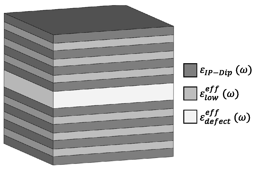
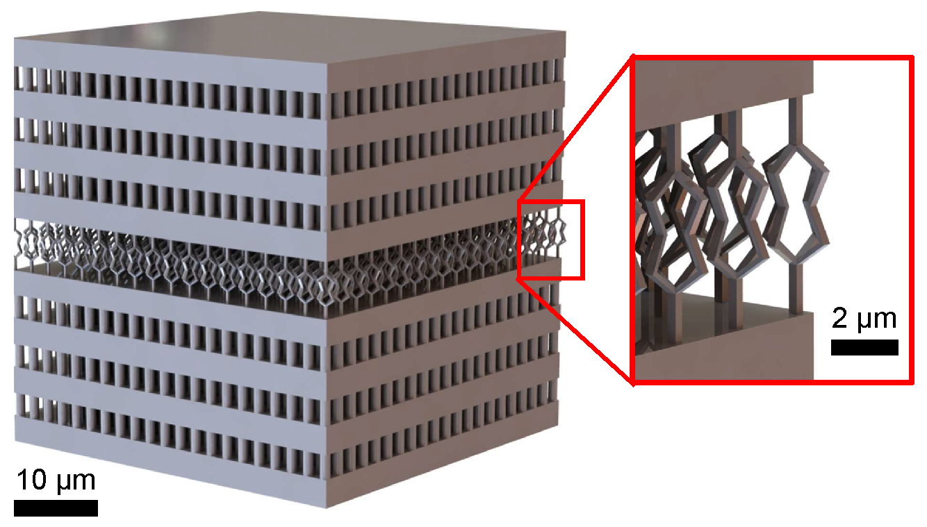
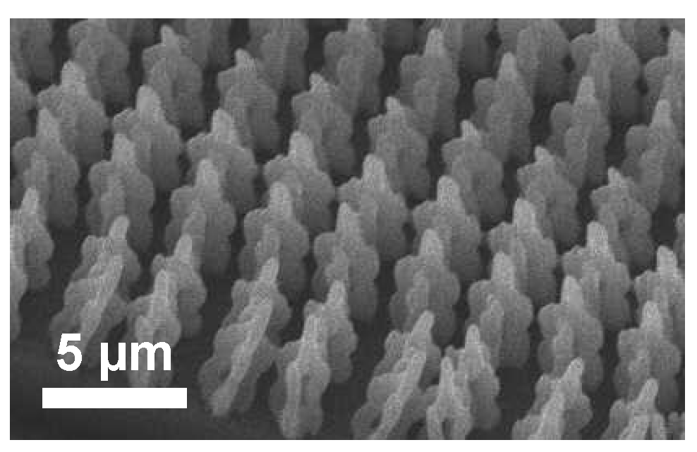
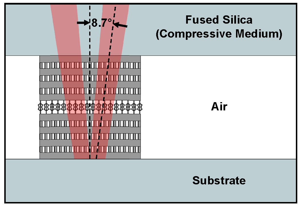
2. Design, Fabrication, and Characterization

A simple stratified layer optical model (WVASE32, J.A. Woolam, Co., Lincoln, NE, USA) was employed to design the one-dimensional photonic crystal. This model calculates the spectral response of a given stratified layer design using the Fresnel equations in conjunction with thin film interference expressions. The photonic crystal is modeled as a stack of three dielectrics. These dielectrics are termed the high-density, low-density and defect layers. The permittivity of the high-density layers, which are composed entirely of a resin compatible with two-photon polymerization (IP-Dip), were taken from Ref. [44]. The permittivity for both the low-density layers and defect layer, as shown in Figure 1, were calculated using the Bruggeman effective medium approximation given by [45]:
ε eff ( ω , f i ) = 1 4 { ( 3 f i 1 ) ε i ( ω ) + ( 2 3 f i ) ε h ( ω ) ± [ ( 3 f i 1 ) ε i ( ω ) + ( 2 3 f i ) ε h ( ω ) ] 2 + ε i ( ω ) ε h ( ω ) 1 2 } .
In this approximation, the effective permittivity for the low-density layers is calculated using the properties of the inclusions ε i and host medium ε h . In this design, the inclusions are composed of the same photosensitive polymer (IP-Dip) as the high-density layers ε i ( ω ) = ε IP Dip ( ω ) . The host medium in this case is air ε h = 1 . The volumetric fill factor f i describes the spatial ratio of inclusions to host medium within these layers. For this approximation to accurately describe the dielectric response of the low-density and defect layers, it is essential that the geometric features within these layers be sub-wavelength.
A geometry was designed such that a photonic bandgap was induced at ω = 2500 cm 1 ( λ = 4 µm), and was, thus, centered in a transparent region for IP-Dip [44]. This geometry can be seen in Figure 2. The designed photonic crystal is composed of 14 alternating layers of high- and low-density with a centralized mechanical defect layer. The nominal thickness of the high-density and low-density layers are 3.35 µm and 2.92 µm, respectively. The low-density layers are composed of an array of sub-wavelength pillars, each with a diameter of 1.20 µm. The pillars are arranged in a square lattice with periodicity of 2.40 µm. The thickness of the defect layer is 6.63 µm. It consists of an array of bow-tie flexures, similar to those shown in Ref. [30], arranged in a square lattice with periodicity of 2.85 µm. Based on these geometries, the volumetric fill factor for the low-density and defect layers were calculated as f i = 0.20 and f i = 0.02 , respectively. The square base of the photonic crystal is 49.2 µm × 49.2 µm.
The designed one-dimensional photonic crystal was fabricated using a commercially available two-photon polymerization system (Photonic Professional GT, Nanoscribe, GmbH, Karlsruhe, Germany). Using this system, the photonic crystal was polymerized on a fused silica substrate. The bow-tie flexures used in the defect layer approached the resolution limits of the two-photon polymerization system. Due to this, it was essential to isolate the bow-tie array to observe the effects of fabrication parameters on the resulting geometry. The optimization method followed in this study was discussed in detail in a previous study, where similar bow-tie flexures were designed for use in the low-density layers of photonic crystals [18].
A dose matrix was performed where scan speed and laser power were varied. Slicing and hatching distances, which define the space between consecutive laser scans, were kept constant at 0.2 µm. SEM images were taken of the dose matrix in order to assess quality. The settings which provided the best results for the flexure layer, as shown in Figure 3, were found to be at a 500 mm/s scan speed and 50% laser power (maximum 25 kW). It can be seen that, for these parameters, the central region of the bow-tie was hollow, allowing the array to flex as designed.
In order to correct for swelling and contraction effects, which occur during fabrication, scaling factors γ SF were applied to the desired nominal layer thicknesses. Conventionally, layer-specific print parameters would need to be used to nullify these effects. The scaling factor approach effectively compensates for the variation in volume-to-surface ratio between the high- and low-density layers without requiring the use of layer-specific print parameters. The scaling factors used for this study were previously determined and verified through SEM imaging [17]. The scaling factors for the high- and low-density layers were γ SF = 0.92 and γ SF = 1.30, respectively.
A transparent window of fused silica was selected to act as the compressive component, in order to provide transparency in the spectral region of the induced photonic bandgap, and, thus, allowing infrared reflection measurements during compression. A 4 × 4 array of the designed photonic crystal was fabricated on the substrate with a square lattice periodicity of 3 mm. Force was applied to the photonic crystals normal to the layer interfaces by placing the window material on the 4 × 4 photonic crystal array. The mass of the window was measured to be 1.37 g. Assuming a uniform force distribution, the applied force per photonic crystal of 0.84 mN was obtained.
Reflection measurements were taken in the infrared spectral range from 2000 cm 1 (5.00 µm) to 3000 cm 1 (3.33 µm), with resolution of 2 cm 1 . A HYPERION 3000 infrared microscope (Bruker, Inc.), in combination with a VERTEX 70 Fourier-transform infrared spectrometer (Bruker, Inc., Billerica, MA, USA), was used for these measurements. A silicon carbide globar was the infrared light source. The 15× Cassegrain objective, with a square 20 µm × 20 µm aperture provided an average angle of incidence of 8.7 ° on the photonic crystal structure with an angular spread of 0.6°. A schematic of the testing apparatus is given in Figure 4. All reflection measurements were taken at room temperature. A bulk gold sample was used to normalize all reflection measurements.

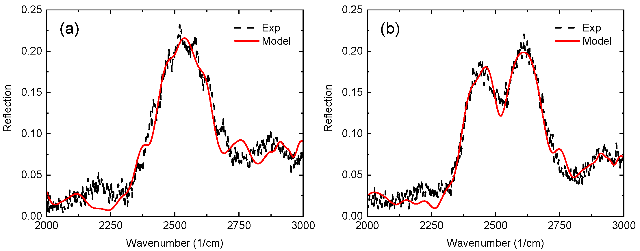
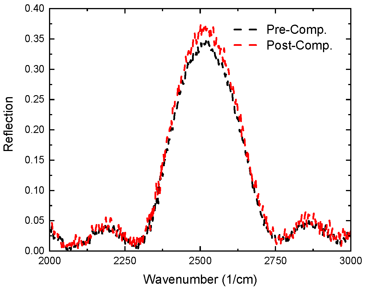
3. Results and Discussion

Experimental Fourier-transform reflection measurements (dashed black) taken during compressive testing and best-model calculated data (solid red) were plotted, and shown in Figure 5. The measurements were taken with the window in place. For the measurements shown in Figure 5a, Kapton tape with a thickness greater than the height of the photonic crystals was placed on the edges of the window to act as a spacer and to prevent compression. In Figure 5b, reflection measurements were taken without this Kapton tape, allowing the window to come in contact with the photonic crystals and compress the structures. Both (a) and (b) show a photonic bandgap centered at 2535 cm 1 . As a 0.84 mN compression was applied to the photonic crystal, defect resonance shifted into the photonic bandgap. Here, a very good agreement could be seen between the experimental data and the best-fit stratified-layer optical model.
The stratified-layer optical model of the design was used to perform the best-fit analysis of the experimental data. The dielectric functions of IP-Dip, the compressive medium and substrate (fused silica) were previously determined using spectroscopic ellipsometry and were not varied in this model [44,46]. A fit analysis was performed by varying geometric model parameters, including the following: high- and low-density layer thicknesses, defect layer thickness, and the volumetric fill factors for both the low-density and defect layers. A Levenberg–Marquardt-based algorithm was used to vary the model parameters until a best-fit was reached between the calculated and the experimental reflection data.
The best-fit model layer thicknesses for the uncompressed photonic crystal (Figure 5a) were determined to be (3.165 ± 0.015) µm for the high-density layer, (2.937 ± 0.026) µm for the low-density layer, and (6.7 ± 0.1) µm for the defect layer. The best-fit volumetric fill factor for the defect layer was determined to be f i = 0.02 ± 0.02. The best-fit model layer thicknesses for the compressed photonic crystal (Figure 5b) were determined to be (3.202 ± 0.033) µm for the high-density layer, (2.844 ± 0.025) µm for the low-density layer, and (4.1 ± 0.1) µm for the defect layer. The best-fit volumetric fill factor for the defect layer was determined to be f i = 0.33 ± 0.08. During the best-model analyses the overall layer thickness non-uniformity and the low-density volumetric fill factor was assumed to be consistent between uncompressed and compressed states. The calculated layer thickness non-uniformity and low-density volumetric fill factor were found to be 4.4 ± 0.7 and f i = 0.41 ± 0.02, respectively.
During compression, the defect layer thickness was calculated and shown to have reduced to (4.1 ± 0.1) µm from (6.7 ± 0.1) µm. Based on this layer displacement, the defect layer, as an array, showed a stiffness of 315 µN/µm to the applied 0.84 mN compression. Since the defect layer consisted of an 18 × 18 array of bow-tie flexures, this suggested the spring constant of a single flexure was roughly 0.97 µN/µm following Hooke’s Law.
To verify elasticity in the defect layer, reflection measurements were taken before and after the compression of the photonic crystal structure. These measurements are given in Figure 6. For this comparison, measurements were taken without the presence of the window. The lack of compressive loading resulted in an increase in bandgap amplitude when compared with the measurements in Figure 5. The black curve in Figure 6 reflects the situation before any compressive contact was made with the photonic crystal structure. The reflection spectra given by the red curve refer to the situation after the compressive load was removed from the photonic crystal structure. The defect-mode resonance which was present during contact (Figure 5b) was no longer located within the photonic bandgap. It can be seen that the amplitude, broadening, and spectral center of the photonic bandgap were very near to those measured before compression (black).

4. Conclusions

A one-dimensional photonic crystal with a mechanical defect layer was fabricated by two-photon polymerization. Under compression, a defect resonance was induced within the observed photonic bandgap. Best-fit analyses of the measured reflection spectra were performed using a simple stratified-layer optical model. Very good agreement between the measured and optical model calculations was observed. The best-fit calculated layer thicknesses were found to be within ±6% when compared with the nominal layer thicknesses. Confidence intervals for the calculated layer thicknesses were comparable to a previous publication, where modeled layer thicknesses were verified by scanning electron microscope imaging [17]. The best-modeled volumetric fill factor for the low-density layers was calculated to be higher than the nominal fill factor. This indicated that the pillar diameters were wider than designed, resulting in the overall larger volume of inclusion material (IP-Dip) within these layers. This may have been a result of swelling effects, which are known to occur during the sample rinsing process [17].
The change in thickness of the defect layer as a result of compression was calculated. This displacement was used to estimate the stiffness of the bow-tie flexures used in the defect layer array. The spring constant of a single bow-tie flexure was calculated to be 0.97 µN/µm. When compared with previously reported microsprings of similar geometric scale fabricated by two-photon polymerization, this spring constant was found to be in the same order of magnitude [47]. It was also observed that the volume fill factor for the defect layer increased during compression. This aligns with expected compression effects. As the layer thickness decreases there is a larger inclusion (IP-Dip) to host medium (air) ratio within this layer.
To verify the elasticity of the defect layer, reflection measurements were taken before and after compressive testing. These measurements verified that the photonic bandgap returns to its original spectral response once compressive force is removed. Changes to the bandgap were unremarkable. These measurements suggest that, after removing the compressive force, the defect layer expands, allowing for the defect resonance to return to its original location, outside the photonic bandgap. Based on this relaxation of the defect layer, composed of a flexible bow-tie array, we suspect this degree of compressive force did not cause appreciable plastic deformation in the photonic crystal.
The observed spectral response, as a result of changes in defect layer thickness, aligned with that of our previous terahertz study [39]. In contrast to the terahertz study, where the defect layer was designed to be an air gap, the defect layer here was attached to the photonic crystal, thus fixing the initial thickness as a result of the bow-tie array geometry. When comparing the degree of defect resonance shifting between these studies, the degree of compression necessary to induce a centralized defect resonance reduced by roughly 50%. Thus, the photonic crystal presented in this study demonstrates a higher sensitivity to changes in layer thickness than what has been previously reported.
The presented results demonstrate the first successful fabrication of a one-dimensional photonic crystal with a mechanically tunable defect, fabricated by means of two-photon polymerization. As designed, the presence of a defect resonance was controlled by applying a compressive force to the photonic crystal structure. Very good agreement was found between the experimental and model calculated data. Using the defect layer thicknesses obtained from performing best-model analyses of the experimental spectra, the mechanical properties of the defect layer were estimated. The calculated mechanical properties of a single flexure agreed with spring constants reported previously for microsprings fabricated by two-photon polymerization from the same material (IP-Dip) on this same geometric scale [47]. Based on the findings of this study, we feel the designed one-dimensional photonic crystal can function as a sensitive mechanical sensor. Such functionality is desired in applications, such as microrobotics, and in MOEMS systems [37].

Author Contributions

Conceptualization, V.P.S., N.S. and T.H.; Formal analysis, V.P.S. and T.H.; Investigation, V.P.S. and T.H.; Methodology, V.P.S. and M.M.; Writing—original draft, V.P.S., D.L., G.D.B. and T.H.; Writing—review & editing, N.S., D.L., M.M. and G.D.B. All authors have read and agreed to the published version of the manuscript.

Funding

This research was funded by the National Science Foundation (2052745) within the IUCRC Center for Metamaterials and through the National Science Foundation MRI (1828430).

Data Availability Statement

The data presented in this study are available on request from the corresponding author.

Acknowledgments

The authors are grateful for support from the National Science Foundation within the IUCRC Center for Metamaterials (2052745), National Science Foundation MRI (1828430), and the Department of Physics and Optical Science of the University of North Carolina at Charlotte.

Conflicts of Interest

The authors declare no conflict of interest.

References

  1. Yue, Y.; Gong, J.P. Tunable one-dimensional photonic crystals from soft materials. J. Photoch. Photobio. C 2015, 23, 45–67. [Google Scholar] [CrossRef]
  2. Steel, M.; Levy, M.; Osgood, R. High transmission enhanced Faraday rotation in one-dimensional photonic crystals with defects. IEEE Photonic Tech. Lett. 2000, 12, 1171–1173. [Google Scholar] [CrossRef]
  3. Shen, H.; Wang, Z.; Wu, Y.; Yang, B. One-dimensional photonic crystals: Fabrication, responsiveness and emerging applications in 3D construction. RSC Adv. 2016, 6, 4505–4520. [Google Scholar] [CrossRef]
  4. Yablonovitch, E. Photonic crystals. J. Mod. Optic. 1994, 41, 173–194. [Google Scholar] [CrossRef]
  5. Tolmachev, V.A.; Baldycheva, A.V.; Berwick, K.; Perova, T.S. Influence of fluctuations of the geometrical parameters on the photonic band gaps in one-dimensional photonic crystals. Prog. Electromagn. Res. 2012, 126, 285–302. [Google Scholar] [CrossRef] [Green Version]
  6. Aly, A.H.; Elsayed, H.A.; Malek, C. Defect modes properties in one-dimensional photonic crystals employing a superconducting nanocomposite material. Opt. Appl. 2018, 48, 53–64. [Google Scholar]
  7. Park, S.; Li, Y.; Norton, B.; McLamb, M.; Boreman, G.D.; Hofmann, T. One-dimensional Photonic Crystals Fabricated Using Stereolithographic Single Layer Assembly for the Terahertz Spectral Range. J. Infrared Millim. Terahertz 2020, 41, 542–551. [Google Scholar] [CrossRef]
  8. Wu, C.J.; Wang, Z.H. Properties of defect modes in one-dimensional photonic crystals. Pr. Electromagn. Res. 2010, 103, 169–184. [Google Scholar] [CrossRef] [Green Version]
  9. John, S. Strong localization of photons in certain disordered dielectric superlattices. Phys. Rev. Lett. 1987, 58, 2486. [Google Scholar] [CrossRef] [Green Version]
  10. Li, Y.; Fullager, D.; Park, S.; Childers, D.; Fesperman, R.; Boreman, G.; Hofmann, T. High-contrast infrared polymer photonic crystals fabricated by direct laser writing. Opt. Lett. 2018, 43, 4711–4714. [Google Scholar] [CrossRef]
  11. Jiang, H.; Chen, H.; Li, H.; Zhang, Y.; Zhu, S. Omnidirectional gap and defect mode of one-dimensional photonic crystals containing negative-index materials. Appl. Phys. Lett. 2003, 83, 5386–5388. [Google Scholar] [CrossRef]
  12. Sánchez, A.; Porta, A.; Orozco, S. Photonic band-gap and defect modes of a one-dimensional photonic crystal under localized compression. J. Appl. Phys. 2017, 121, 173101. [Google Scholar] [CrossRef]
  13. Scotognella, F.; Chiasera, A.; Criante, L.; Aluicio-Sarduy, E.; Varas, S.; Pelli, S.; Łukowiak, A.; Righini, G.C.; Ramponi, R.; Ferrari, M. Metal oxide one dimensional photonic crystals made by RF sputtering and spin coating. Ceram. Int. 2015, 41, 8655–8659. [Google Scholar] [CrossRef]
  14. Langer, R.; Barski, A.; Simon, J.; Pelekanos, N.; Konovalov, O.; Andre, R.; Dang, L.S. High-reflectivity GaN/GaAlN Bragg mirrors at blue/green wavelengths grown by molecular beam epitaxy. Appl. Phys. Lett. 1999, 74, 3610–3612. [Google Scholar] [CrossRef]
  15. Rybin, M.V.; Shishkin, I.I.; Samusev, K.B.; Belov, P.A.; Kivshar, Y.S.; Kiyan, R.V.; Chichkov, B.N.; Limonov, M.F. Band structure of photonic crystals fabricated by two-photon polymerization. Crystals 2015, 5, 61–73. [Google Scholar] [CrossRef]
  16. Houbertz, R.; Declerck, P.; Passinger, S.; Ovsianikov, A.; Serbin, J.; Chichkov, B. Investigations on the generation of photonic crystals using two-photon polymerization (2PP) of inorganic–organic hybrid polymers with ultra-short laser pulses. Phys. Status Solidi A 2007, 204, 3662–3675. [Google Scholar] [CrossRef]
  17. Stinson, V.P.; Park, S.; McLamb, M.; Boreman, G.; Hofmann, T. Photonic Crystals with a Defect Fabricated by Two-Photon Polymerization for the Infrared Spectral Range. Optics 2021, 2, 284–291. [Google Scholar] [CrossRef]
  18. Stinson, V.P.; Shuchi, N.; McLamb, M.; Boreman, G.D.; Hofmann, T. Mechanical Control of the Optical Bandgap in One-Dimensional Photonic Crystals. Micromachines 2022, 13, 2248. [Google Scholar] [CrossRef]
  19. Park, S.; Li, Y.; McLamb, M.; Norton, B.; Boreman, G.D.; Hofmann, T. Highly Localized Defect Mode in Polymer-Based THz Photonic Crystals Fabricated Using Stereolithography. J. Infrared Millim. Terahertz 2020, 41, 825–833. [Google Scholar] [CrossRef]
  20. Park, S.; Norton, B.; Boreman, G.D.; Hofmann, T. Mechanical tuning of the terahertz photonic bandgap of 3D-printed one-dimensional photonic crystals. J. Infrared Millim. Terahertz 2021, 42, 220–228. [Google Scholar] [CrossRef]
  21. Aly, A.H.; Elsayed, H.A. Defect mode properties in a one-dimensional photonic crystal. Physica B 2012, 407, 120–125. [Google Scholar] [CrossRef]
  22. Lee, H.Y.; Yao, T. Design and evaluation of omnidirectional one-dimensional photonic crystals. J. Appl. Phys. 2003, 93, 819–830. [Google Scholar] [CrossRef]
  23. Vinogradov, A.; Dorofeenko, A.; Erokhin, S.; Inoue, M.; Lisyansky, A.; Merzlikin, A.; Granovsky, A. Surface state peculiarities in one-dimensional photonic crystal interfaces. Phys. Rev. B 2006, 74, 045128. [Google Scholar] [CrossRef] [Green Version]
  24. Wan, B.F.; Zhou, Z.W.; Xu, Y.; Zhang, H.F. A theoretical proposal for a refractive index and angle sensor based on one-dimensional photonic crystals. IEEE Sens. J. 2020, 21, 331–338. [Google Scholar] [CrossRef]
  25. Nelson, R.; Haus, J. One-dimensional photonic crystals in reflection geometry for optical applications. Appl. Phys. Lett. 2003, 83, 1089–1091. [Google Scholar] [CrossRef]
  26. Juodkazis, S.; Mizeikis, V.; Seet, K.K.; Misawa, H.; Wegst, U.G. Mechanical properties and tuning of three-dimensional polymeric photonic crystals. Appl. Phys. Lett. 2007, 91, 241904. [Google Scholar] [CrossRef]
  27. Zhang, R.; Wang, Q.; Zheng, X. Flexible mechanochromic photonic crystals: Routes to visual sensors and their mechanical properties. J. Mater. Chem. C 2018, 6, 3182–3199. [Google Scholar] [CrossRef]
  28. Xia, J.; Qiao, Q.; Zhou, G.; Chau, F.S.; Zhou, G. Opto-mechanical photonic crystal cavities for sensing application. Appl. Sci. 2020, 10, 7080. [Google Scholar] [CrossRef]
  29. Jansen, C.; Wietzke, S.; Astley, V.; Mittleman, D.M.; Koch, M. Mechanically flexible polymeric compound one-dimensional photonic crystals for terahertz frequencies. Appl. Phys. Lett. 2010, 96, 111108. [Google Scholar] [CrossRef] [Green Version]
  30. Jayne, R.K.; Stark, T.J.; Reeves, J.B.; Bishop, D.J.; White, A.E. Dynamic Actuation of Soft 3D Micromechanical Structures Using Micro-Electromechanical Systems (MEMS). Adv. Mater. Technol. 2018, 3, 1700293. [Google Scholar] [CrossRef]
  31. Ding, L.; Li, Y.; Zhou, C.; Hu, M.; Xiong, Y.; Zeng, Z. In-fiber Mach-Zehnder interferometer based on three-core fiber for measurement of directional bending. Sensors 2019, 19, 205. [Google Scholar] [CrossRef] [PubMed] [Green Version]
  32. Jindal, S.K.; Raghuwanshi, S.K.; Kumar, A. Realization of MOEMS pressure sensor using mach zehnder interferometer. J. Mech. Sci. Technol. 2015, 29, 3831–3839. [Google Scholar] [CrossRef]
  33. Agarwal, S.; Mishra, J.K.; Priye, V. Highly sensitive MOEMS integrated photonic crystal cavity resonator for nano-mechanical sensing. Opt. Commun. 2020, 474, 126150. [Google Scholar] [CrossRef]
  34. Chaudhary, V.S.; Kumar, D.; Mishra, R.; Sharma, S. Hybrid dual core photonic crystal fiber as hydrostatic pressure sensor. Optik 2020, 210, 164497. [Google Scholar] [CrossRef]
  35. Rajasekar, R.; Robinson, S. Nano-pressure and temperature sensor based on hexagonal photonic crystal ring resonator. Plasmonics 2019, 14, 3–15. [Google Scholar] [CrossRef]
  36. Nguyen, L.V.; Schartner, E.P.; Otten, D.; Yu, Z.; Lancaster, D.; Ebendorff-Heidepriem, H.; Warren-Smith, S.C. Multi-point optical fiber pressure sensor. In Proceedings of the AOS Australian Conference on Optical Fibre Technology (ACOFT) and Australian Conference on Optics, Lasers, and Spectroscopy (ACOLS) 2019, Melbourne, Australia, 9–12 December 2019; Volume 11200, pp. 40–41. [Google Scholar]
  37. Lao, Z.; Xia, N.; Wang, S.; Xu, T.; Wu, X.; Zhang, L. Tethered and Untethered 3D Microactuators Fabricated by Two-Photon Polymerization: A Review. Micromachines 2021, 12, 465. [Google Scholar] [CrossRef]
  38. Upadhyaya, A.M.; Hasan, M.K.; Abdel-Khalek, S.; Hassan, R.; Srivastava, M.C.; Sharan, P.; Islam, S.; Saad, A.M.E.; Vo, N. A comprehensive review on the optical micro-electromechanical sensors for the biomedical application. Front. Public Health 2021, 9, 759032. [Google Scholar] [CrossRef]
  39. Park, S.; Stinson, V.P.; McLamb, M.; Boreman, G.D.; Hofmann, T. Mechanical tuning of defect modes in polymer-based terahertz one-dimensional photonic crystals fabricated by stereolithography. Opt. Eng. 2021, 60, 117104. [Google Scholar] [CrossRef]
  40. Calin, B.S.; Paun, I.A. A Review on Stimuli-Actuated 3D Micro/Nanostructures for Tissue Engineering and the Potential of Laser-Direct Writing via Two-Photon Polymerization for Structure Fabrication. Int. J. Mol. Sci. 2022, 23, 14270. [Google Scholar] [CrossRef]
  41. Păun, I.A.; Mustăciosu, C.C.; Popescu, R.C.; Călin, B.Ş.; Mihăilescu, M. Collagen/chitosan functionalization of complex 3d structures fabricated by laser direct writing via two-photon polymerization for enhanced osteogenesis. Int. J. Mol. Sci. 2020, 21, 6426. [Google Scholar] [CrossRef]
  42. Paun, I.A.; Zamfirescu, M.; Luculescu, C.R.; Acasandrei, A.M.; Mustaciosu, C.C.; Mihailescu, M.; Dinescu, M. Electrically responsive microreservoires for controllable delivery of dexamethasone in bone tissue engineering. Appl. Surf. Sci. 2017, 392, 321–331. [Google Scholar] [CrossRef]
  43. Joya, Y.F.; Wang, T.; Liu, Z. Formation and antibacterial activities of nanostructured TiO2 based thin films by sol-gel/laser-induced technique. In Proceedings of the International Congress on Applications of Lasers & Electro-Optics, Orlando, FL, USA, 23–27 October 2011; Volume 2011, pp. 1152–1160. [Google Scholar]
  44. Fullager, D.B.; Boreman, G.D.; Hofmann, T. Infrared dielectric response of nanoscribe IP-dip and IP-L monomers after polymerization from 250 cm−1 to 6000 cm−1. Opt. Mater. Express 2017, 7, 888–894. [Google Scholar] [CrossRef]
  45. Cai, W.; Shalaev, V.M. Optical Metamaterials; Springer: Berlin/Heidelberg, Germany, 2010; Volume 10. [Google Scholar]
  46. Li, Y.; Fullager, D.; Angelbello, E.; Childers, D.; Boreman, G.; Hofmann, T. Broadband near-infrared antireflection coatings fabricated by three-dimensional direct laser writing. Opt. Lett. 2018, 43, 239–242. [Google Scholar] [CrossRef] [PubMed] [Green Version]
  47. Shang, X.; Wang, N.; Wang, Z.; Jiang, H.; Jia, Y.; Zhou, N.; Qiu, M. Customizable and highly sensitive 3D micro-springs produced by two-photon polymerizations with improved post-treatment processes. Appl. Phys. Lett. 2022, 120, 171107. [Google Scholar] [CrossRef]
Figure 1. The spatial layer arrangements and layer permittivities used to model the optical response of the designed photonic crystal can be seen. Permittivities with the superscript “eff” are calculated using the Bruggeman effective medium approximation given in Equation (1). The permittivity with a subscript “IP-Dip” is used for the high-density layers which are composed entirely of the photosensitive polymer used in this study.
Optics 04 00021 g001
Figure 2. CAD model of the designed one-dimensional photonic crystal under study. The photonic crystal is composed of 14 alternating layers of high- and low-density with a centralized mechanical defect layer. The nominal thicknesses of the high-density, low-density, and defect layers were modeled to be 3.35 µm, 2.92 µm, and 6.63 µm, respectively.
Optics 04 00021 g002
Figure 3. Scanning electron microscope image of an array of mechanical flexures. This array was fabricated with a scan speed of 500 mm/s at 50% laser power (max 25 kW). The periodic arrangement of this array matched that of the mechanical defect layer in Figure 2.
Optics 04 00021 g003
Figure 4. Cross-sectional schematic of the one-dimensional photonic crystal during compressive testing. The compressive medium (fused silica) is shown in contact with the photonic crystal structure. The photonic crystal is illuminated by a Cassegrain objective. For the 20 µm × 20 µm square aperture setting the average angle of incidence on the sample was 8.7 ° with an angular spread of 0.6°, shown here as the red beam path regions. This illumination was radially symmetric with respect to the normal axis.
Optics 04 00021 g004
Figure 5. Experimental reflection measurements (black dashed lines) taken before (a) and during (b) compression of the photonic crystal and best-fit models (red solid lines). Measurements were taken through the fused silica window. The feature dominating the spectra was the photonic bandgap, which was centered around 2535 cm 1 . During compression, a transmissive defect resonance was observed within the photonic bandgap. The experimental and best-model calculated reflection data were in good agreement.
Optics 04 00021 g005
Figure 6. Experimental reflection measurements of the photonic crystals before (black) and after (red) compressive testing. Both measurements were taken in air, without the presence of the fused silica window. A slight amplitude change was observed as a result of the compressive testing. No other spectral changes to the photonic bandgap were distinguishable.
Optics 04 00021 g006
Disclaimer/Publisher’s Note: The statements, opinions and data contained in all publications are solely those of the individual author(s) and contributor(s) and not of MDPI and/or the editor(s). MDPI and/or the editor(s) disclaim responsibility for any injury to people or property resulting from any ideas, methods, instructions or products referred to in the content.

