
Optimized Design and Simulation of Optical Section in Electro-Reflective Modulators Based on Photonic Crystals Integrated with Multi-Quantum-Well Structures

Abstract
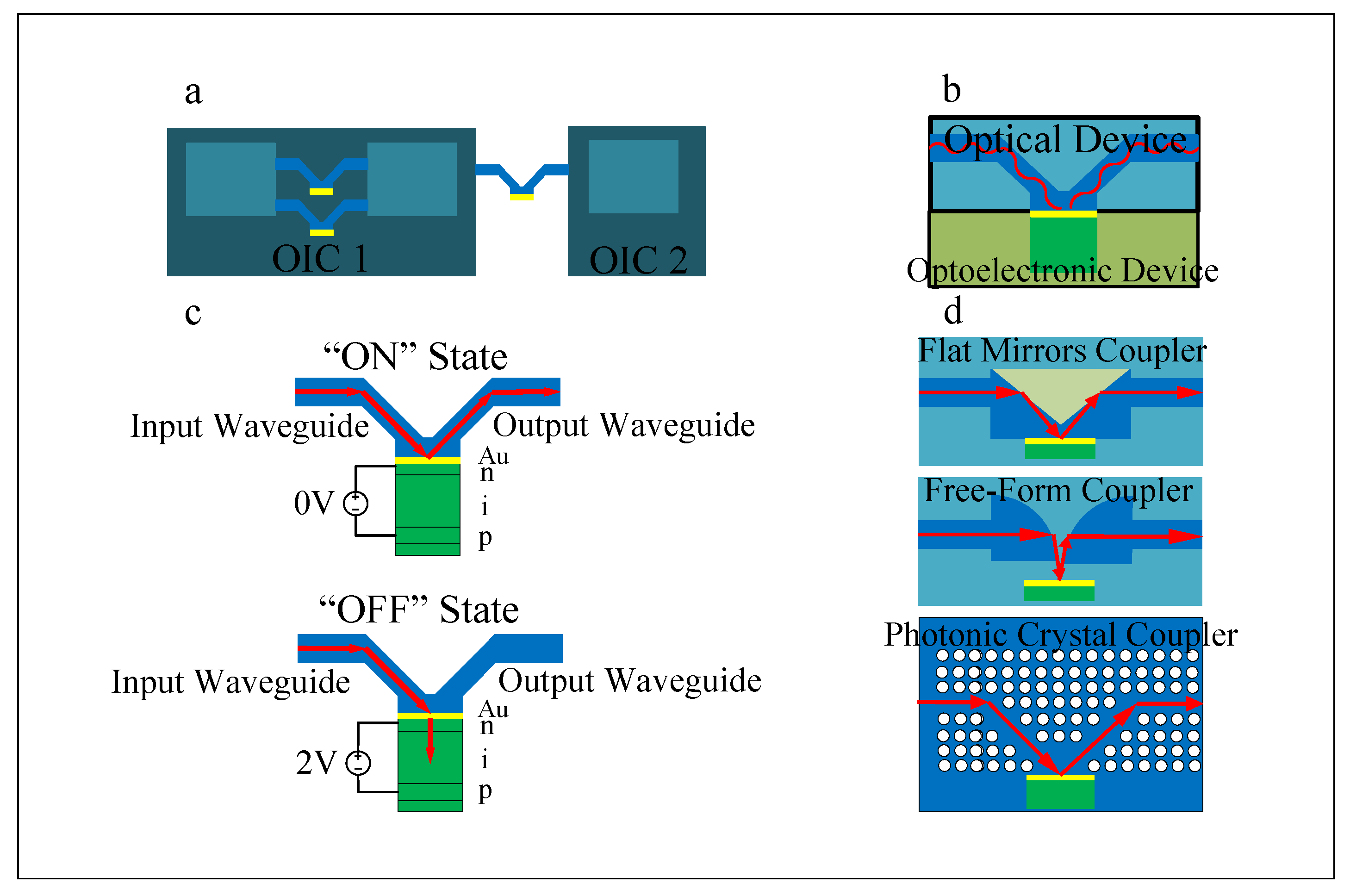
:1. Introduction
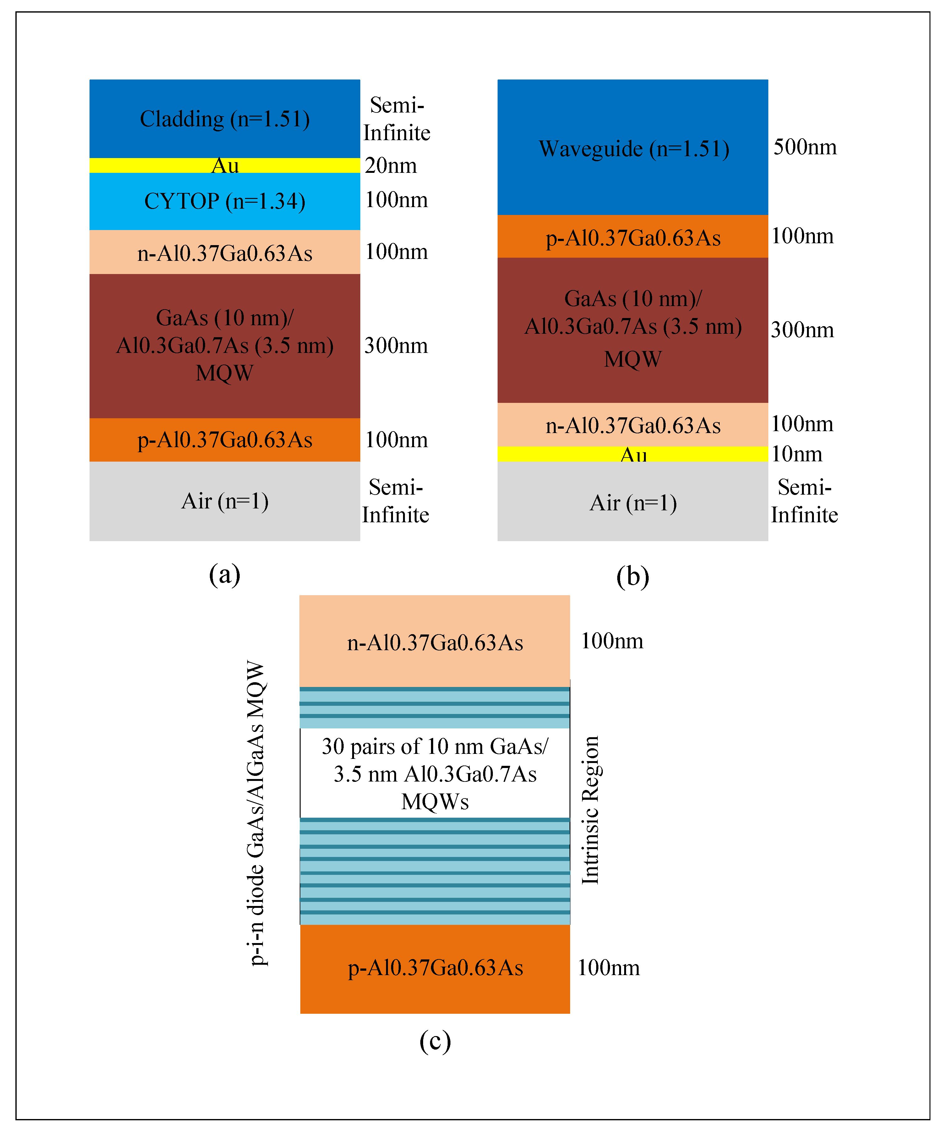
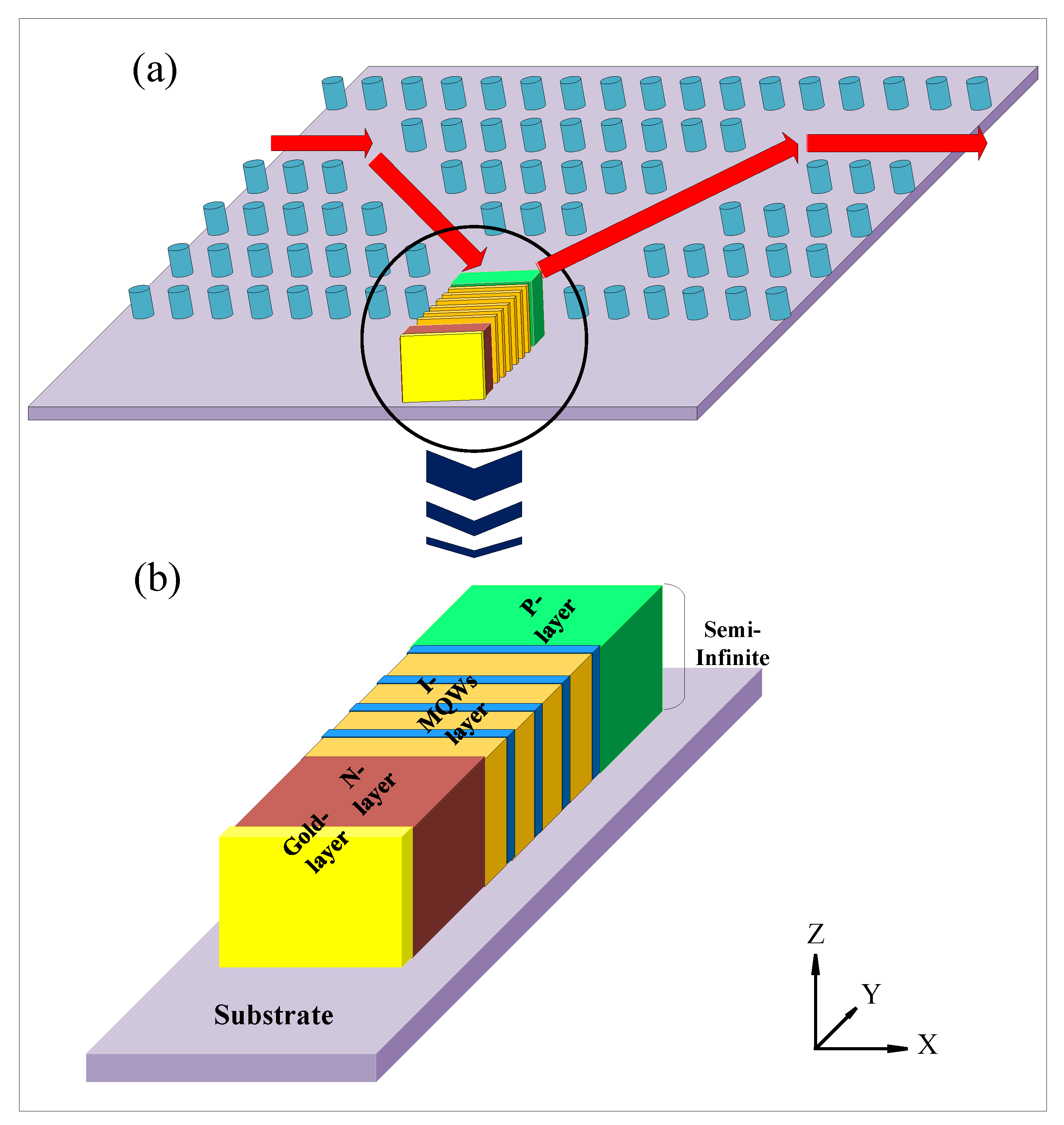
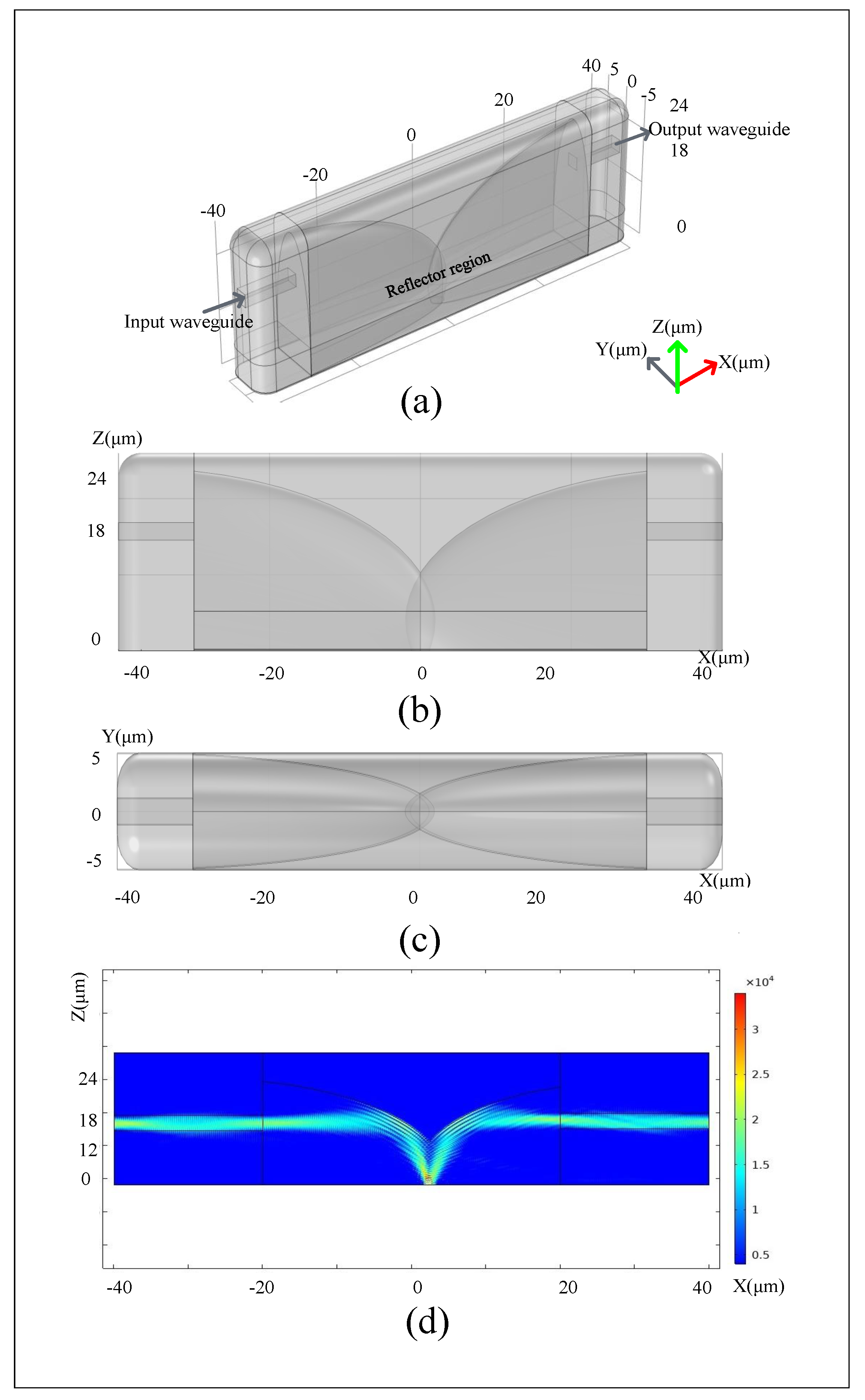
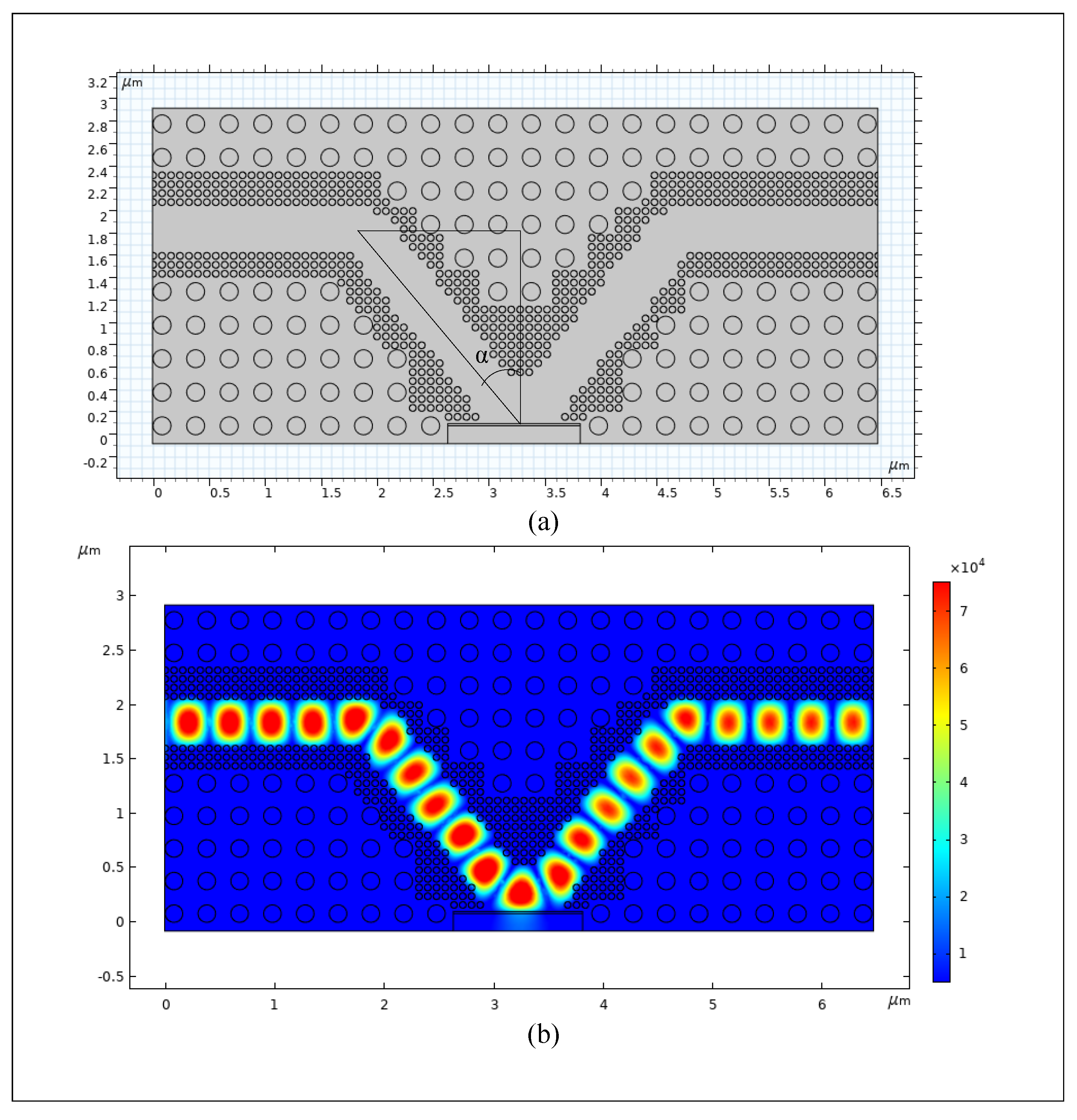
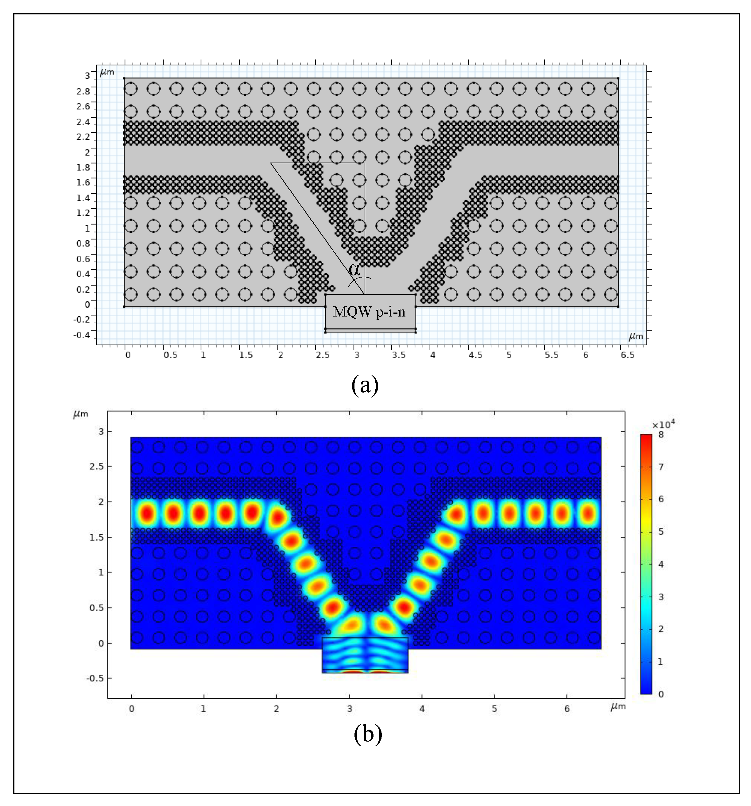
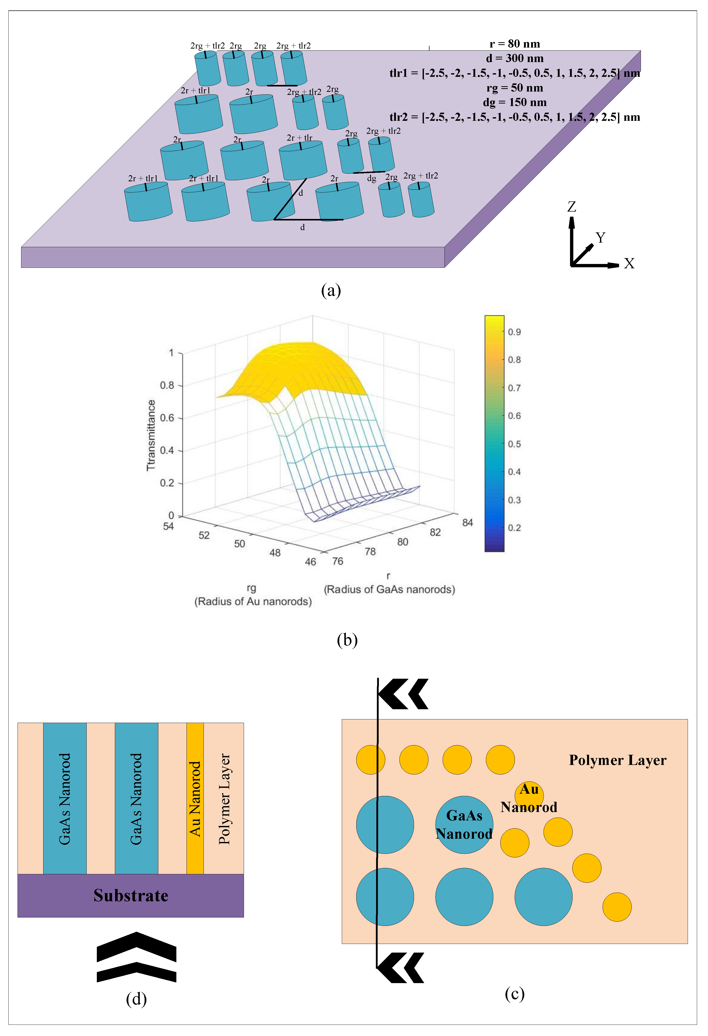
2. Conceptual Design
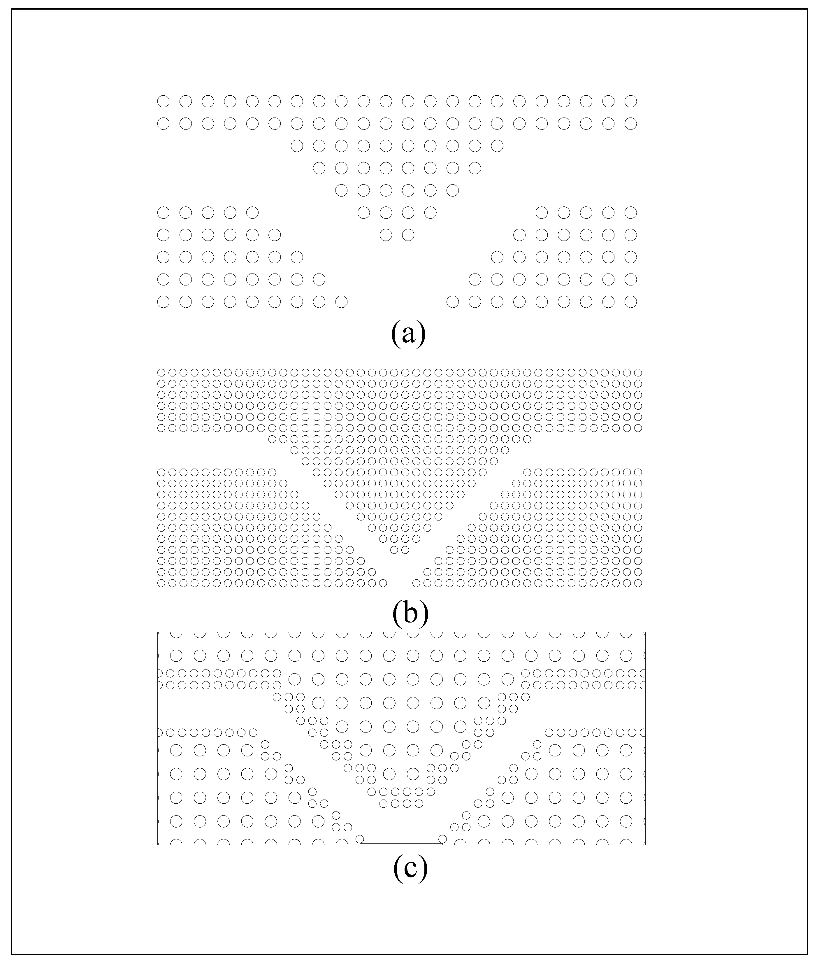
3. The Design of Electro-Reflective Photonic Crystals Modulators
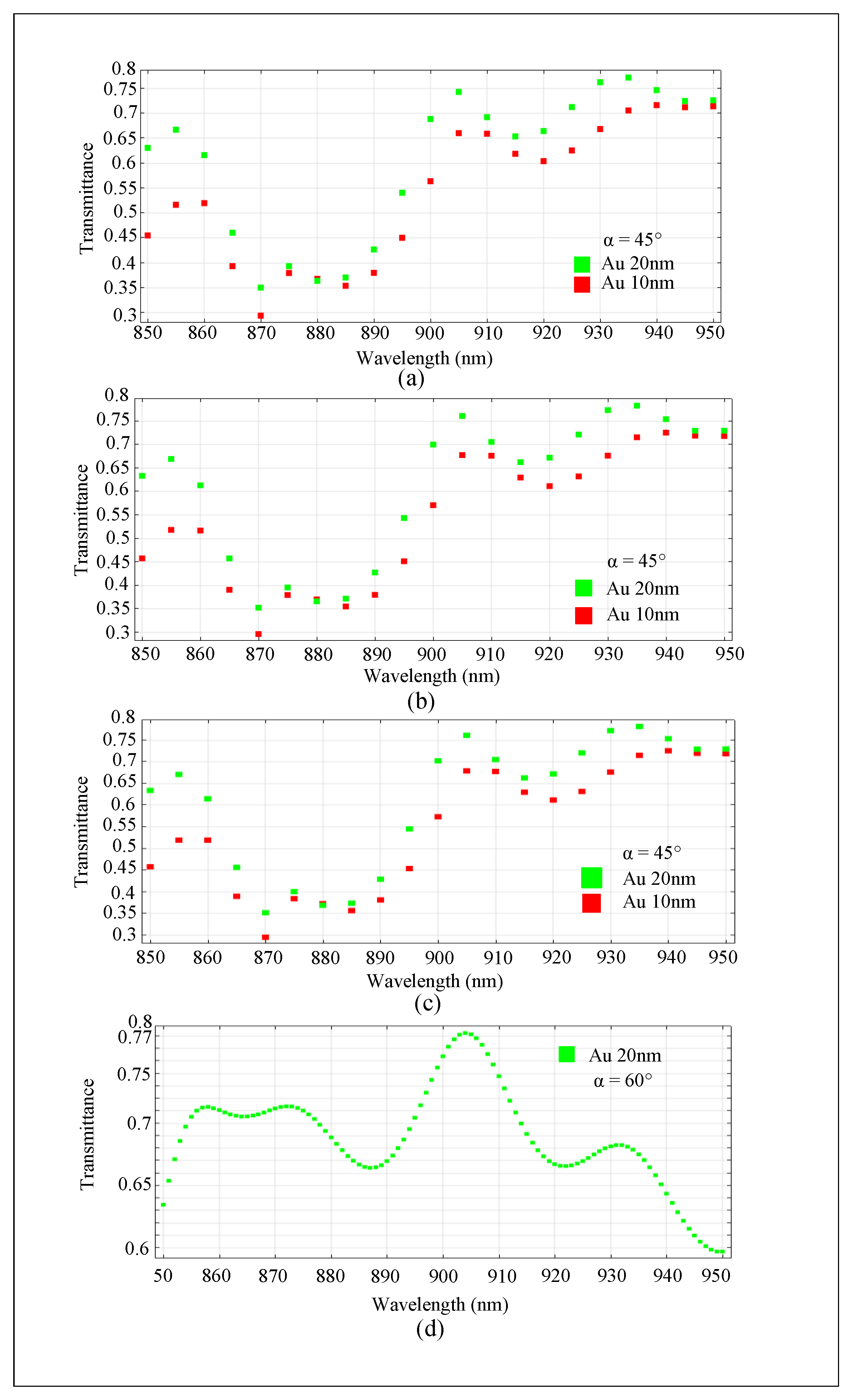
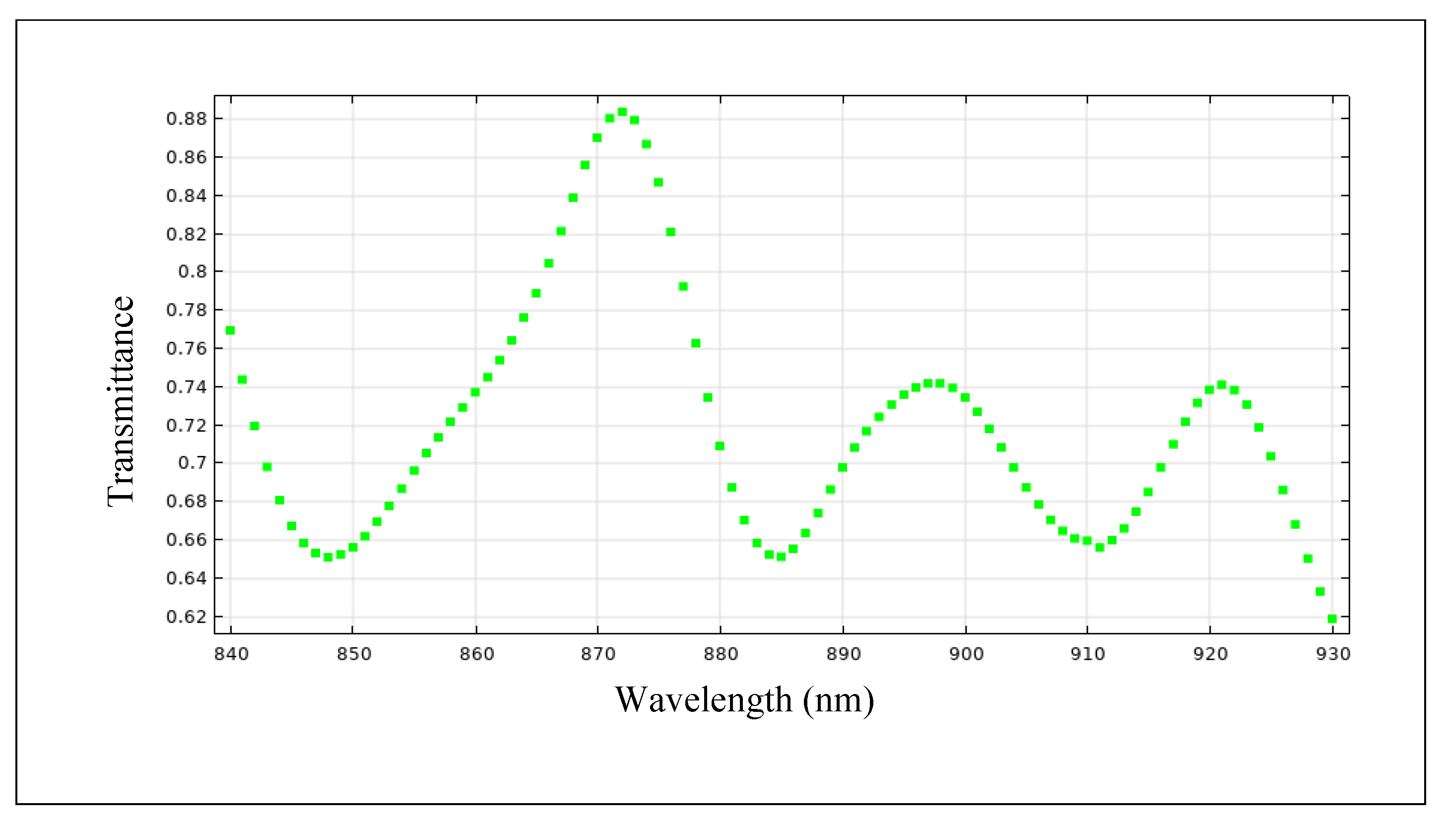
4. Results and Discussion
5. Conclusions
Author Contributions
Funding
Data Availability Statement
Conflicts of Interest
References
- Wang, X.; Liu, J. Emerging technologies in Si active photonics. J. Semicond. 2018, 39, 061001. [Google Scholar] [CrossRef]
- Shen, Y.; Meng, X.; Cheng, Q.; Rumley, S.; Abrams, N.; Gazman, A.; Manzhosov, E.; Glick, M.S.; Bergman, K. Silicon photonics for extreme scale systems. J. Light. Technol. 2019, 37, 245–259. [Google Scholar]
- Yu, S.; Zuo, H.; Wang, X.; Sun, X.; Liu, J.; Hu, J.; Gu, T. Seamless hybrid-integrated interconnect network (SHINE). In Proceedings of the 2019 Optical Fiber Communications Conference and Exhibition (OFC), San Diego, CA, USA, 3–7 March 2019; IEEE: Piscataway, NJ, USA, 2019; pp. 1–3. [Google Scholar]
- Yu, S.; Zuo, H.; Sun, X.; Liu, J.; Gu, T.; Hu, J. Optical Free-form couplers for high-density integrated photonics (OFFCHIP): A universal optical interface. J. Light. Technol. 2020, 38, 3358–3365. [Google Scholar] [CrossRef]
- Han, S.P.; Kim, J.T.; Jung, S.W.; Ahn, S.H.; Choi, C.G.; Jeong, M.Y. A reflective curved mirror with low coupling loss for optical interconnection. IEEE Photonics Technol. Lett. 2004, 16, 185–187. [Google Scholar] [CrossRef]
- Dangel, R.; Hofrichter, J.; Horst, F.; Jubin, D.; La Porta, A.; Meier, N.; Soganci, I.M.; Weiss, J.; Offrein, B.J. Polymer waveguides for electro-optical integration in data centers and high-performance computers. Opt. Express 2015, 23, 4736–4750. [Google Scholar] [CrossRef] [PubMed]
- Mikawa, T.; Kinoshita, M.; Hiruma, K.; Ishitsuka, T.; Okabe, M.; Hiramatsu, S.; Furuyama, H.; Matsui, T.; Kumai, K.; Ibaragi, O.; et al. Implementation of active interposer for high-speed and low-cost chip level optical interconnects. IEEE J. Sel. Top. Quantum Electron. 2003, 9, 452–459. [Google Scholar]
- Li, L.; Zou, Y.; Lin, H.; Hu, J.; Sun, X.; Feng, N.N.; Danto, S.; Richardson, K.; Gu, T.; Haney, M. A fully-integrated flexible photonic platform for chip-to-chip optical interconnects. J. Light. Technol. 2013, 31, 4080–4086. [Google Scholar] [CrossRef]
- Nieweglowski, K.; Lorenz, L.; Lüngen, S.; Tiedje, T.; Wolter, K.J.; Bock, K. Optical coupling with flexible polymer waveguides for chip-to-chip interconnects in electronic systems. Microelectron. Reliab. 2018, 84, 121–126. [Google Scholar]
- Barwicz, T.; Taira, Y.; Lichoulas, T.W.; Boyer, N.; Martin, Y.; Numata, H.; Nah, J.W.; Takenobu, S.; Janta-Polczynski, A.; Kimbrell, E.L.; et al. A novel approach to photonic packaging leveraging existing high-throughput microelectronic facilities. IEEE J. Sel. Top. Quantum Electron. 2016, 22, 455–466. [Google Scholar] [CrossRef]
- Hu, J.; Li, L.; Lin, H.; Zhang, P.; Zhou, W.; Ma, Z. Flexible integrated photonics: Where materials, mechanics and optics meet. Opt. Mater. Express 2013, 3, 1313–1331. [Google Scholar]
- Hiramatsu, S.; Mikawa, T. Optical design of active interposer for high-speed chip level optical interconnects. J. Light. Technol. 2006, 24, 927. [Google Scholar] [CrossRef]
- Cho, I.K.; Lee, W.J.; Rho, B.S.; Jeong, M.Y. Polymer waveguide with integrated reflector mirrors for an inter-chip link system. Opt. Commun. 2008, 281, 4906–4909. [Google Scholar] [CrossRef]
- Ogunsola, O.; Thacker, H.; Bachim, B.; Bakir, M.; Pikarsky, J.; Gaylord, T.K.; Meindl, J. Chip-level waveguide-mirror-pillar optical interconnect structure. IEEE Photonics Technol. Lett. 2006, 18, 1672–1674. [Google Scholar] [CrossRef]
- Lin, X.; Hosseini, A.; Dou, X.; Subbaraman, H.; Chen, R.T. Low-cost board-to-board optical interconnects using molded polymer waveguide with 45 degree mirrors and inkjet-printed micro-lenses as proximity vertical coupler. Opt. Express 2013, 21, 60–69. [Google Scholar] [CrossRef] [PubMed]
- Li, G.; Yao, J.; Thacker, H.; Mekis, A.; Zheng, X.; Shubin, I.; Luo, Y.; Lee, J.H.; Raj, K.; Cunningham, J.E.; et al. Ultralow-loss, high-density SOI optical waveguide routing for macrochip interconnects. Opt. Express 2012, 20, 12035–12039. [Google Scholar] [CrossRef] [PubMed]
- Geng, Q.; Wang, D.; Chen, P.; Chen, S.C. Ultrafast multi-focus 3-D nano-fabrication based on two-photon polymerization. Nat. Commun. 2019, 10, 2179. [Google Scholar] [CrossRef] [Green Version]
- Saha, S.K.; Wang, D.; Nguyen, V.H.; Chang, Y.; Oakdale, J.S.; Chen, S.C. Scalable submicrometer additive manufacturing. Science 2019, 366, 105–109. [Google Scholar] [CrossRef]
- Faraji Rad, Z.; Prewett, P.D.; Davies, G.J. High-resolution two-photon polymerization: The most versatile technique for the fabrication of microneedle arrays. Microsyst. Nanoeng. 2021, 7, 71. [Google Scholar] [CrossRef]
- Borisov, R.; Dorojkina, G.; Koroteev, N.; Kozenkov, V.; Magnitskii, S.; Malakhov, D.; Tarasishin, A.; Zheltikov, A. Fabrication of three-dimensional periodic microstructures by means of two-photon polymerization. Appl. Phys. B Lasers Opt. 1998, 67, 765. [Google Scholar] [CrossRef]
- Serbin, J.; Egbert, A.; Ostendorf, A.; Chichkov, B.; Houbertz, R.; Domann, G.; Schulz, J.; Cronauer, C.; Fröhlich, L.; Popall, M. Femtosecond laser-induced two-photon polymerization of inorganic–organic hybrid materials for applications in photonics. Opt. Lett. 2003, 28, 301–303. [Google Scholar] [CrossRef]
- Serbin, J.; Ovsianikov, A.; Chichkov, B. Fabrication of woodpile structures by two-photon polymerization and investigation of their optical properties. Opt. Express 2004, 12, 5221–5228. [Google Scholar] [CrossRef] [PubMed] [Green Version]
- Liu, Y.; Wang, H.; Ho, J.; Ng, R.C.; Ng, R.J.; Hall-Chen, V.H.; Koay, E.H.; Dong, Z.; Liu, H.; Qiu, C.W.; et al. Structural color three-dimensional printing by shrinking photonic crystals. Nat. Commun. 2019, 10, 4340. [Google Scholar] [CrossRef] [PubMed] [Green Version]
- Lindenmann, N.; Balthasar, G.; Hillerkuss, D.; Schmogrow, R.; Jordan, M.; Leuthold, J.; Freude, W.; Koos, C. Photonic wire bonding: A novel concept for chip-scale interconnects. Opt. Express 2012, 20, 17667–17677. [Google Scholar] [CrossRef] [PubMed] [Green Version]
- Billah, M.R.; Blaicher, M.; Hoose, T.; Dietrich, P.I.; Marin-Palomo, P.; Lindenmann, N.; Nesic, A.; Hofmann, A.; Troppenz, U.; Moehrle, M.; et al. Hybrid integration of silicon photonics circuits and InP lasers by photonic wire bonding. Optica 2018, 5, 876–883. [Google Scholar] [CrossRef]
- Lindenmann, N.; Dottermusch, S.; Goedecke, M.L.; Hoose, T.; Billah, M.R.; Onanuga, T.P.; Hofmann, A.; Freude, W.; Koos, C. Connecting silicon photonic circuits to multicore fibers by photonic wire bonding. J. Light. Technol. 2014, 33, 755–760. [Google Scholar] [CrossRef] [Green Version]
- Gissibl, T.; Thiele, S.; Herkommer, A.; Giessen, H. Two-photon direct laser writing of ultracompact multi-lens objectives. Nat. Photonics 2016, 10, 554–560. [Google Scholar] [CrossRef]
- Toulouse, A.; Thiele, S.; Giessen, H.; Herkommer, A.M. Alignment-free integration of apertures and nontransparent hulls into 3D-printed micro-optics. Opt. Lett. 2018, 43, 5283–5286. [Google Scholar] [CrossRef] [Green Version]
- Gissibl, T.; Thiele, S.; Herkommer, A.; Giessen, H. Sub-micrometre accurate free-form optics by three-dimensional printing on single-mode fibres. Nat. Commun. 2016, 7, 11763. [Google Scholar] [CrossRef] [Green Version]
- Dietrich, P.I.; Blaicher, M.; Reuter, I.; Billah, M.; Hoose, T.; Hofmann, A.; Caer, C.; Dangel, R.; Offrein, B.; Troppenz, U.; et al. In situ 3D nanoprinting of free-form coupling elements for hybrid photonic integration. Nat. Photonics 2018, 12, 241–247. [Google Scholar] [CrossRef] [Green Version]
- Gordillo, O.A.J.; Chaitanya, S.; Chang, Y.C.; Dave, U.D.; Mohanty, A.; Lipson, M. Plug-and-play fiber to waveguide connector. Opt. Express 2019, 27, 20305–20310. [Google Scholar] [CrossRef]
- Wang, X.; Yu, S.; Zuo, H.; Sun, X.; Hu, J.; Gu, T.; Liu, J. Design of hybrid plasmonic multi-quantum-well electro-reflective modulators towards< 100 fJ/bit photonic links. IEEE J. Sel. Top. Quantum Electron. 2020, 27, 1–8. [Google Scholar]
- Wang, X.; Yu, S.; Qin, J.; Cuervo-Covian, A.; Zuo, H.; Sun, X.; Hu, J.; Gu, T.; Liu, J. Low-voltage, coupled multiple quantum well electroreflective modulators towards ultralow power inter-chip optical interconnects. J. Light. Technol. 2020, 38, 3414–3421. [Google Scholar] [CrossRef]
- Rafiee, E.; Emami, F.; Negahdari, R. Design of a novel nano plasmonic-dielectric photonic crystal power splitter suitable for photonic integrated circuits. Optik 2018, 172, 234–240. [Google Scholar] [CrossRef]
- Negahdari, R.; Rafiee, E.; Emami, F.; Pakarzadeh, H. Design of tunable ring-shaped plasmonic photonic crystal filters infiltrated with optical fluids. Opt. Eng. 2021, 60, 097102. [Google Scholar] [CrossRef]
- Askarian, A.; Akbarizadeh, G.; Fartash, M. A novel proposal for all optical half-subtractor based on photonic crystals. Opt. Quantum Electron. 2019, 51, 1–9. [Google Scholar] [CrossRef]
- Rafiee, E.; Emami, F. Realization of tunable optical channel drop filter based on photonic crystal octagonal shaped structure. Optik 2018, 171, 798–802. [Google Scholar] [CrossRef]
- Hajshahvaladi, L.; Kaatuzian, H.; Moghaddasi, M.; Danaie, M. Hybridization of surface plasmons and photonic crystal resonators for high-sensitivity and high-resolution sensing applications. Sci. Rep. 2022, 12, 21292. [Google Scholar] [CrossRef]
- Veisi, E.; Seifouri, M.; Olyaee, S. Ultra-compact and Fast All-optical Photonic Crystal Half-subtractor Logic Gate. In Proceedings of the 2022 30th International Conference on Electrical Engineering (ICEE), Tehran, Iran, 17–19 May 2022; IEEE: Piscataway, NJ, USA, 2022; pp. 869–873. [Google Scholar]
- Parandin, F.; Sheykhian, A. Design of an all-optical half adder based on photonic crystal ring resonator. Opt. Quantum Electron. 2022, 54, 443. [Google Scholar] [CrossRef]
- Moshfe, S.; Abedi, K.; Moravvej-Farshi, M.K. Fully integrated 3-bit all-optical analog to digital converter based on photonic crystal semiconductor optical amplifier. Opt. Laser Technol. 2022, 148, 107773. [Google Scholar] [CrossRef]
- Hong, Y.H.; Miao, W.C.; Hsu, W.C.; Hong, K.B.; Lin, C.L.; Lin, C.; Chen, S.C.; Kuo, H.C. Progress of photonic-crystal surface-emitting lasers: A paradigm shift in LiDAR application. Crystals 2022, 12, 800. [Google Scholar] [CrossRef]
- Reilly, K.J.; Kalapala, A.; Song, A.; Rotter, T.; Liu, Z.; Renteria, E.; Fan, S.; Zhou, W.; Balakrishnan, G. Fabrication of Photonic Crystal Surface Emitting Lasers (PCSELs) by Epitaxial Regrowth. In Proceedings of the CLEO: QELS_Fundamental Science, San Jose, CA, USA, 9–14 May 2021; Optica Publishing Group: Washington, DC, USA, 2021; p. JTu3A.78. [Google Scholar]
- Reilly, K.J.; Kalapala, A.; Yeom, S.; Addamane, S.J.; Renteria, E.; Zhou, W.; Balakrishnan, G. Epitaxial regrowth and hole shape engineering for photonic crystal surface emitting lasers (PCSELs). J. Cryst. Growth 2020, 535, 125531. [Google Scholar] [CrossRef]
- Zhou, X.; Ma, X.; Zhao, S.; Qu, H.; Qi, A.; Zheng, W. Photonic crystal diode laser arrays integrated with a phase shifter designed for narrow far-field angle. In Proceedings of the 2018 Conference on Lasers and Electro-Optics (CLEO), San Jose, CA, USA, 13–18 May 2018; IEEE: Piscataway, NJ, USA, 2018; pp. 1–2. [Google Scholar]
- Kamran, M.; Abedi, K.; Sharifi, M.J. Novel multi-stage photonic crystal Mach-Zehnder optical filters. IEEE Photonics Technol. Lett. 2018, 30, 1874–1877. [Google Scholar] [CrossRef]
- Rajasekar, R.; Raja, G.T.; Robinson, S. Numerical investigation of reconfigurable photonic crystal switch based on phase change nanomaterial. IEEE Trans. Nanotechnol. 2020, 19, 545–552. [Google Scholar] [CrossRef]
- Kazanskiy, N.L.; Butt, M.A.; Khonina, S.N. 2D-Heterostructure photonic crystal formation for on-chip polarization division multiplexing. Photonics 2021, 8, 313. [Google Scholar] [CrossRef]
- Li, M.; Ling, J.; He, Y.; Javid, U.A.; Xue, S.; Lin, Q. Lithium niobate photonic-crystal electro-optic modulator. Nat. Commun. 2020, 11, 4123. [Google Scholar] [CrossRef]
- Fathi, F.; Rashidi, M.R.; Pakchin, P.S.; Ahmadi-Kandjani, S.; Nikniazi, A. Photonic crystal based biosensors: Emerging inverse opals for biomarker detection. Talanta 2021, 221, 121615. [Google Scholar] [CrossRef]
- Shi, C.; Yuan, J.; Luo, X.; Shi, S.; Lu, S.; Yuan, P.; Xu, W.; Chen, Z.; Yu, H. Transmission characteristics of multi-structure bandgap for lithium niobate integrated photonic crystal and waveguide. Opt. Commun. 2020, 461, 125222. [Google Scholar] [CrossRef]
- Zhang, C.; Yoshimi, H.; Ota, Y.; Iwamoto, S. Two-dimensional Topological Photonic Crystals with Helical Edge States below the Light Line. In Proceedings of the 2021 26th Microoptics Conference (MOC), Hamamatsu, Japan, 26–29 September 2021; IEEE: Piscataway, NJ, USA, 2021; pp. 1–2. [Google Scholar]
- Yoshimi, H.; Yamaguchi, T.; Ota, Y.; Arakawa, Y.; Iwamoto, S. Slow light waveguides in topological valley photonic crystals. Opt. Lett. 2020, 45, 2648–2651. [Google Scholar] [CrossRef]
- Dong, G.; Yang, X.; Cai, L.; Shen, X.; Wang, Y. Improvement of transmission properties through two-bend resonance by holographic design for a two-dimemsional photonic crystal waveguide. Opt. Express 2008, 16, 15375–15381. [Google Scholar] [CrossRef]
- Iwamoto, S.; Ota, Y.; Arakawa, Y. Recent progress in topological waveguides and nanocavities in a semiconductor photonic crystal platform. Opt. Mater. Express 2021, 11, 319–337. [Google Scholar] [CrossRef]
- Tokushima, M.; Ushida, J.; Gomyo, A.; Shirane, M.; Yamada, H. Efficient transmission mechanisms for waveguides with 90 bends in pillar photonic crystals. JOSA B 2005, 22, 2472–2479. [Google Scholar] [CrossRef]
- Vishnoi, A.; Mudi, R.; Debnath, K. Systematic design study of waveguides and waveguide bends in diamond-structured photonic crystals. JOSA B 2021, 38, 907–913. [Google Scholar] [CrossRef]
- Robin, Y.; Bae, S.; Shubina, T.; Pristovsek, M.; Evropeitsev, E.; Kirilenko, D.; Davydov, V.Y.; Smirnov, A.; Toropov, A.; Jmerik, V.; et al. Insight into the performance of multi-color InGaN/GaN nanorod light emitting diodes. Sci. Rep. 2018, 8, 7311. [Google Scholar] [CrossRef] [PubMed] [Green Version]
- Glukhov, I.A.; Dadoenkova, Y.S.; Bentivegna, F.F.; Moiseev, S.G. Deterministic aperiodic photonic crystal with a 2D array of metallic nanoparticles as polarization-sensitive dichroic filter. J. Appl. Phys. 2020, 128, 053101. [Google Scholar] [CrossRef]
- Wang, H.C.; Martin, O.J. Polarization-Controlled Chromo-Encryption. Adv. Opt. Mater. 2023, 2202165. [Google Scholar] [CrossRef]
- Zhang, L.; Chang, S.; Chen, X.; Ding, Y.; Rahman, M.T.; Duan, Y.; Stephen, M.; Ni, X. High-Efficiency, 80 mm Aperture Metalens Telescope. Nano Lett. 2022. [Google Scholar] [CrossRef]
- Heshmati, M.M.K.; Emami, F. Numerical Investigations of 2-D Optical Free-Form Couplers for Surface Connections of Photonic Integrated Circuits. Results Opt. 2023, 10, 100351. [Google Scholar] [CrossRef]


Disclaimer/Publisher’s Note: The statements, opinions and data contained in all publications are solely those of the individual author(s) and contributor(s) and not of MDPI and/or the editor(s). MDPI and/or the editor(s) disclaim responsibility for any injury to people or property resulting from any ideas, methods, instructions or products referred to in the content. |
© 2023 by the authors. Licensee MDPI, Basel, Switzerland. This article is an open access article distributed under the terms and conditions of the Creative Commons Attribution (CC BY) license (https://creativecommons.org/licenses/by/4.0/).
Share and Cite
Heshmati, M.M.K.; Emami, F. Optimized Design and Simulation of Optical Section in Electro-Reflective Modulators Based on Photonic Crystals Integrated with Multi-Quantum-Well Structures. Optics 2023, 4, 227-245. https://doi.org/10.3390/opt4010016
Heshmati MMK, Emami F. Optimized Design and Simulation of Optical Section in Electro-Reflective Modulators Based on Photonic Crystals Integrated with Multi-Quantum-Well Structures. Optics. 2023; 4(1):227-245. https://doi.org/10.3390/opt4010016
Chicago/Turabian StyleHeshmati, Mohammad Mahdi Khakbaz, and Farzin Emami. 2023. "Optimized Design and Simulation of Optical Section in Electro-Reflective Modulators Based on Photonic Crystals Integrated with Multi-Quantum-Well Structures" Optics 4, no. 1: 227-245. https://doi.org/10.3390/opt4010016