Article

Compact Optical System Based on Scatterometry for Off-Line and Real-Time Monitoring of Surface Micropatterning Processes

by
Marcos Soldera
1,*,
Sascha Teutoburg-Weiss
1,
Nikolai Schröder
1,
Bogdan Voisiat
1 and
Andrés Fabián Lasagni
1,2
1
Institut für Fertigungstechnik, Technische Universität Dresden, George-Bähr-Str. 3c, 01069 Dresden, Germany
2
Fraunhofer-Institut für Werkstoff- und Strahltechnik IWS, Winterbergstr. 28, 01277 Dresden, Germany
*
Author to whom correspondence should be addressed.
Optics 2023, 4(1), 198-213; https://doi.org/10.3390/opt4010014
Submission received: 11 November 2022 / Revised: 6 January 2023 / Accepted: 23 February 2023 / Published: 24 February 2023
(This article belongs to the Section Laser Sciences and Technology)

Abstract

:
In this study, a scatterometry-based monitoring system designed for tracking the quality and reproducibility of laser-textured surfaces in industrial environments was validated in off-line and real-time modes. To this end, a stainless steel plate was structured by direct laser interference patterning (DLIP) following a set of conditions with artificial patterning errors. Namely, fluctuations of the DLIP process parameters such as laser fluence, spatial period, and focus position are introduced, and also, two patterning strategies are implemented, whereby pulses are deliberately not fired at both deterministic and random positions. The detection limits of the system were determined by recording the intensities of the zero, first, and second diffraction order using a charge-coupled device (CCD) camera. As supported by topographical measurements, the system can accurately calculate spatial periods with a resolution of at least 100 nm. In addition, focus shifts of 70 µm from the optimum focus position can be detected, and missing patterned lines with a minimum width of 28 µm can be identified. The validation of this compact characterization unit represents a step forward for its implementation as an in-line monitoring tool for industrial laser-based micropatterning.

1. Introduction

Laser-based manufacturing methods offer an attractive combination of traits such as a high degree of flexibility, processability of a wide range of materials, high throughput, and direct processing without the need for masks, photoresists, or post treatments [1,2]. Surface functionalization by modifying the material’s topography using laser ablation, i.e., melting, has become very popular in the scientific community [3,4,5]. Several laser micro/nanotexturing techniques have been developed in the last decades for this purpose, such as direct laser writing (DLW) [6], laser-induced periodic surface structuring (LIPSS) [7], and direct laser interference patterning (DLIP) [8]. The latter method is based on the overlap of two or more laser beams onto the sample surface to produce an interference pattern, whereby the material can be ablated or melted at the maxima positions, leaving a repetitive topography on the surface. The geometry of the resulting texture can be easily controlled by the number of interfering beams, their polarization, and their azimuthal and elevation angles [9,10]. Furthermore, the texture’s spatial period can be fine-tuned by adjusting the overlapping angle between the beams and the used wavelength [11]. The DLIP technique stands out for its unique combination of flexibility, high throughput, and resolution down to the sub-micron scale [8]. However, to bring DLIP to large-scale manufacturing, an effective process monitoring scheme needs to be developed to ensure high-quality and reproducible microtextures.
Several approaches based on different physical mechanisms have been implemented to monitor laser-based surface texturing. For instance, the heat emitted as electromagnetic radiation by the treated surface during the laser processing can be characterized using infrared (IR) cameras. In this direction, Tran and co-workers estimated the deposited thermal energy using ultra-short pulses on silicon and steel by IR imaging. Their image analysis revealed that approximately two-thirds of the laser energy was transformed into heat, which is a significant amount that needs to be considered for optimizing the process efficiency [12,13]. Furthermore, IR cameras were used to monitor the heat accumulation in a DLIP process and to establish a correlation between the camera signal and surface texture quality [14,15]. In addition, the radiation emitted in the visible and near-infrared spectra can be recorded using photodiodes and analyzed to monitor process variables such as laser power or pulse repetition rate [16]. Another strategy to keep track of the process stability is analyzing the acoustic signals produced during the laser ablation. In this regard, Stauter et al. measured and modeled the shock wave produced during the ablation of ceramic materials and linked the ablation rate to the signal detected by a microphone [17]. In another work, the acoustic signal captured during a DLIP treatment was used not only to detect fluctuations in the focus position but also to estimate deviations in the produced spatial period of the topography [18].
The pattern formed on a screen by light reflected from a structured surface can be used as a “fingerprint” of the texture if certain conditions are met. For instance, by illuminating a microstructured surface with a coherent and monochromatic light source, the produced speckle pattern can be collected with a charge-coupled device (CCD) camera and analyzed to calculate the arithmetical mean roughness (Ra) of the surface [19]. In a similar approach, imaging systems to capture the diffraction patterns reflected from periodic or quasi-periodic surface textures have been developed and extensively studied. In this method, commonly known as scatterometry, the captured images are compared to analytical or numerical models to extract useful information from the surface, such as texture shape, spatial periods, structure height, or texture uniformity. There is a plethora of available modeling techniques for complementing the experimental data, for instance, rigorous couple-wave analysis (RCWA) [20,21], Fourier modal method (FMM) [22,23], finite-difference time-domain (FDTD) [24,25], or finite element method (FEM) [26,27], all of which are numerical rigorous models. Simpler yet effective analytical models based on Fourier optics or even the well-known grating equation can also be used for benchmarking the experimental data [28,29]. Scatterometry was successfully used to characterize LIPSS on stainless steel and to detect fluctuations in the spatial periods of LIPSS when the fluence and angle of incidence were varied [30]. In a recent work done by our group, a compact imaging system that can be easily integrated as an in-line monitoring unit was presented and used to record the diffraction patterns from DLIP-treated samples. The images were analyzed, accurately yielding the spatial period and providing information on texture homogeneity [15,31,32]. However, there are still several aspects of the method that need to be further tested to validate it as a reliable and practical monitoring system for DLIP texturing. Therefore, this study sought to investigate the detection limits of the method upon introducing patterning errors on the sample surface, to evaluate the acquired images when DLIP parameters are varied, and to extract useful information upon fluctuations in the process parameters.

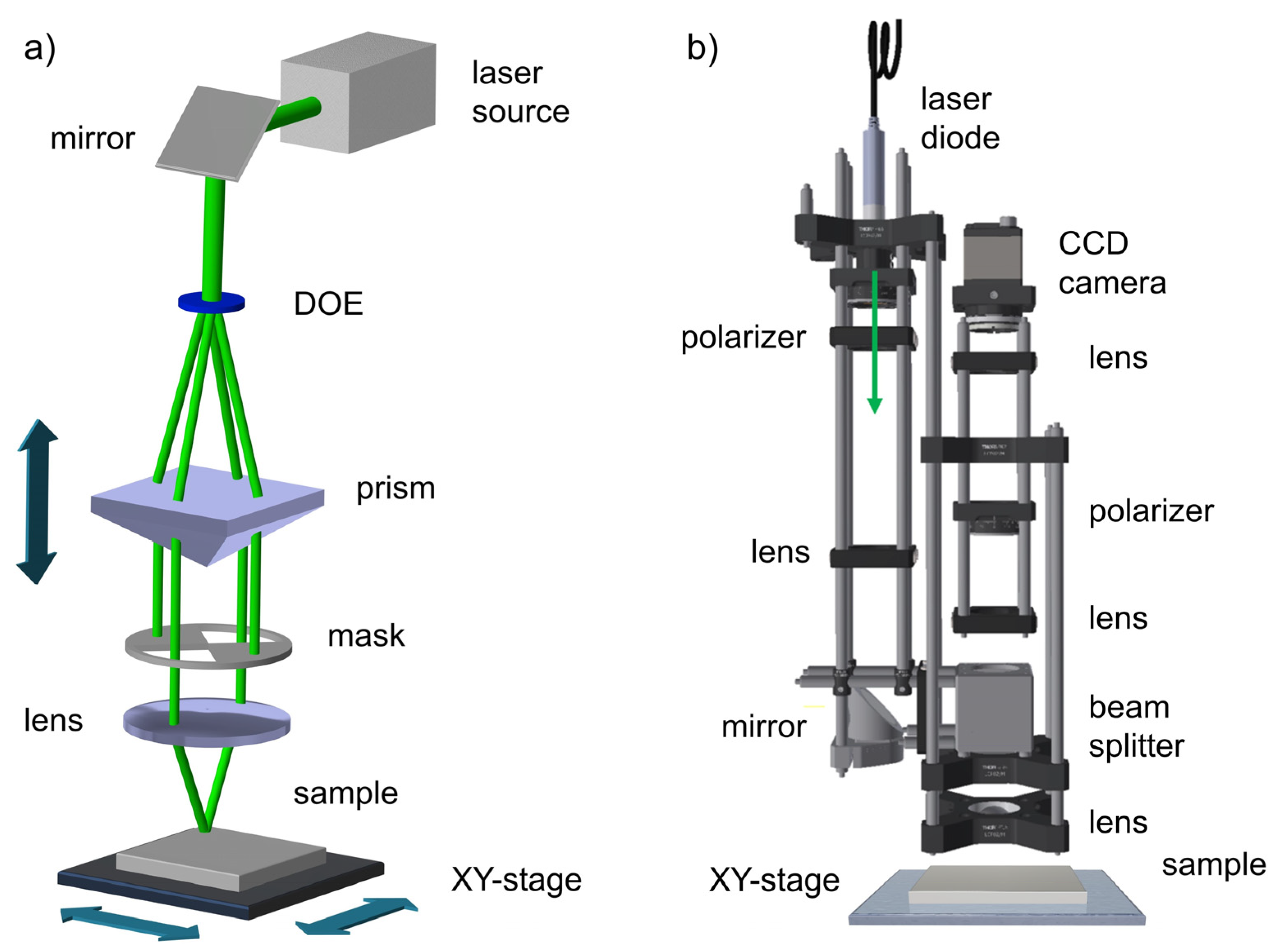
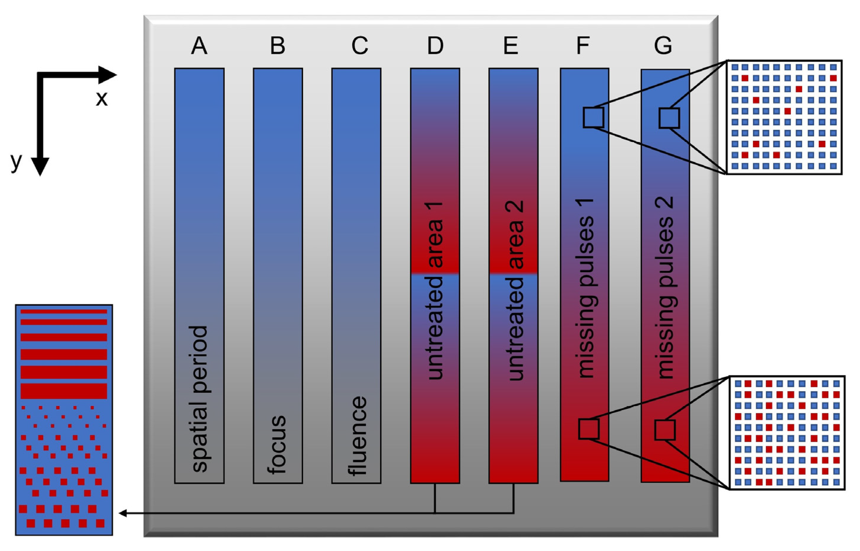
2. Materials and Methods

An electro-polished stainless steel plate with a size of 100 × 100 mm2, a thickness of 1 mm, and an initial roughness (Ra) of 52 nm (according to DIN-ISO 25178 norm) was used for the DLIP structuring experiments.
The steel surface was structured with a DLIP system, as shown schematically in Figure 1a, equipped with a ps-pulsed solid-state laser (neoLASE, Hannover, Germany) and emitting a maximum average power of 7.5 W at a wavelength λ = 532 nm. The pulse length of the system is fixed at 70 ps, the maximum pulse energy at the sample was 30 µJ at a 10 kHz repetition rate, and the spot diameter was 50 µm. As displayed in Figure 1a, the DLIP optics (Fraunhofer IWS, Dresden, Germany) splits the incoming beam from the laser source into four sub-beams, which are then parallelized by a prism and focused on the sample by a converging lens. For the experiments performed in this work, two beams were blocked, while the remaining two beams were overlapped, resulting in a 1D interference pattern. The spatial period Λ can be easily adjusted by changing the overlapping angle between the two beams 2α according to Equation (1) [11]:
Λ = λ 2 sin α .
In the used system, the overlapping angle was controlled by moving the prism relative to the converging lens [33].
Five different experiments were designed in order to test the capability of the monitoring unit to detect errors during the DLIP process. In each of these experiments, either a single DLIP parameter was varied, or some pulses were not fired during the structuring sequence to leave unstructured or partially structured areas with different geometries on the sample. For benchmarking the results, a reference texture was produced at a laser fluence of 0.75 J/cm2, a pulse-to-pulse feed of 7.0 µm, a hatch distance of 15.0 µm, a repetition rate of 10 kHz, and an overlapping angle 2α = 10.2°, yielding a nominal spatial period of 3.0 µm. A total of seven samples was produced on the steel plate, and in each sample, different parameters or different strategies were applied to induce artificial errors or fluctuations in the process (see schematics in Figure 2 and Table 1 for details). The five set of experiments are described as follows.
The first factor under study was the spatial period of the line-like texture, which was modified by changing the overlapping angle of the beams. A total of 11 fields with an area of 7 × 7 mm2 was structured with calculated spatial periods ranging from 1.3 to 3.3 µm (sample A in Table 1). The minimum spatial period of 1.3 µm was selected because this is the minimum spatial period that the monitoring system can detect according to previous simulations [31], whereas the maximum used period is imposed by the limitation of the current DLIP setup.
In sample B, the focus position was changed from −310 to 310 µm relative to the optimum focus position used in the reference texture (positive values mean a closer distance to the DLIP optics). Additionally, 11 fields with a size of 7 × 7 mm2 were produced with varying focus shifts.
In sample C, the impact of fluence variations in the topography and measured signals was investigated by changing the fluence from 0.03 to 0.75 J/cm2. In this case, 12 fields with an area of 7 × 7 mm2 were structured.
In the fourth set of experiments, corresponding to samples D and E, some areas were deliberately left unstructured by programming the laser controller to avoid firing pulses at given positions. Namely, in samples D and E, two patterning geometries were applied: (i) in the top half of both samples, complete horizontal gaps were left unstructured with increasing gap widths from top to bottom (see Figure 2), and (ii) in the bottom half section, square-shaped areas were left untreated, also with increasing size from the top to bottom (see Figure 2). The difference between samples D and E is that in sample E, the gaps and squares have significantly smaller dimensions (see Table 1).
Finally, in the fifth set of experiments, the laser was prevented from firing single pulses at discrete random positions. In sample F, a pulse-to-pulse feed of 7 µm and hatch distance of 15 µm was maintained as in the previous samples, and in each of the 12 structured fields, each with a size of 7 × 7 mm2, the probability of missing pulses increases linearly from top to bottom (see Table 1). In turn, sample G was patterned with a different strategy; namely, the pulse-to-pulse feed and hatch distance were set equal to the spot size, i.e., 50 µm, to avoid overlap between adjacent pulses. In addition, at each position, 10 pulses were applied. As in sample F, the probability of missing spots was increased from the top structured field to the one at the bottom (see Table 1). Although the probability of missing pulses in samples F and G is equivalent, these samples were processed with different structuring strategies that are commonly used in DLIP. The monitoring capabilities as a function of each strategy were thus tested.
The topography of the structured samples was characterized by optical confocal microscopy (Sensofar S Neox, Barcelona, Spain) using a 150× objective providing a lateral and vertical resolution of 140 nm and 1 nm, respectively.
The monitoring system is based on the principle of diffraction, whereby light reflecting from a periodic micropatterned surface is split into multiple diffraction angles, i.e., modes, according to the well-known grating equation [28]. By collecting the resulting diffraction pattern characteristic of the surface under study, valuable information can be extracted from the intensity, shape, and position of the diffraction orders. The used monitoring system is schematically shown in Figure 1b and consists of a low-power laser diode (532 nm), a CCD camera to capture the diffraction pattern, polarization optics to adjust the intensity of light arriving at the sample and camera, and a set of lenses for collecting the light from the surface and focusing it on the camera sensor. The measured spot diameter at the sample surface was approximately 1 mm, resulting in several tens of thousands of DLIP-produced microstructures that are illuminated at the same time. In this way, well-defined diffraction modes can be collected with the optical system. A detailed description of the device can be found elsewhere [31]. For recording the surface diffraction patterns, the samples were moved under the monitoring system with a hexapod stage (Aerotech HEX500-350 HL, Pittsburgh, PA, USA). The samples were measured (i) off-line, in which videos were recorded, and afterwards, they were analyzed to extract data, and (ii) in real-time, where data were extracted frame after frame from the captured images. Before measuring each sample, the laser spot of the monitoring system was positioned at the top-most edge, i.e., y = 0 (as defined in Figure 2). Then, the sample was moved along the y-direction at a constant speed until reaching the bottom edge of the sample, while the CCD camera recorded a video with the measured diffraction pattern. The CCD camera was connected via USB port to a laptop (Intel core i5-5257U, 8 GB RAM, running on Microsoft Windows 10, Redmond, WA, USA). Finally, each frame of the video was analyzed to extract useful information from the laser-patterned samples and, particularly, to detect the errors during the laser process. To this end, the images were first converted to grayscale pixels and then to binary white/black images by thresholding them at a level of 65 in the grayscale. Afterward, the images were dilated to detect the contour of the different orders, and finally, the area of each order was calculated using Green’s theorem. The images were processed with self-programmed codes based on OpenCV library [34]. The measurements were repeated three times. For the off-line experiments, the axis speed was set at 5 mm/s, while the camera frame rate was 79 fps. In the case of the real-time evaluation, the axis speed and frame rate were varied.

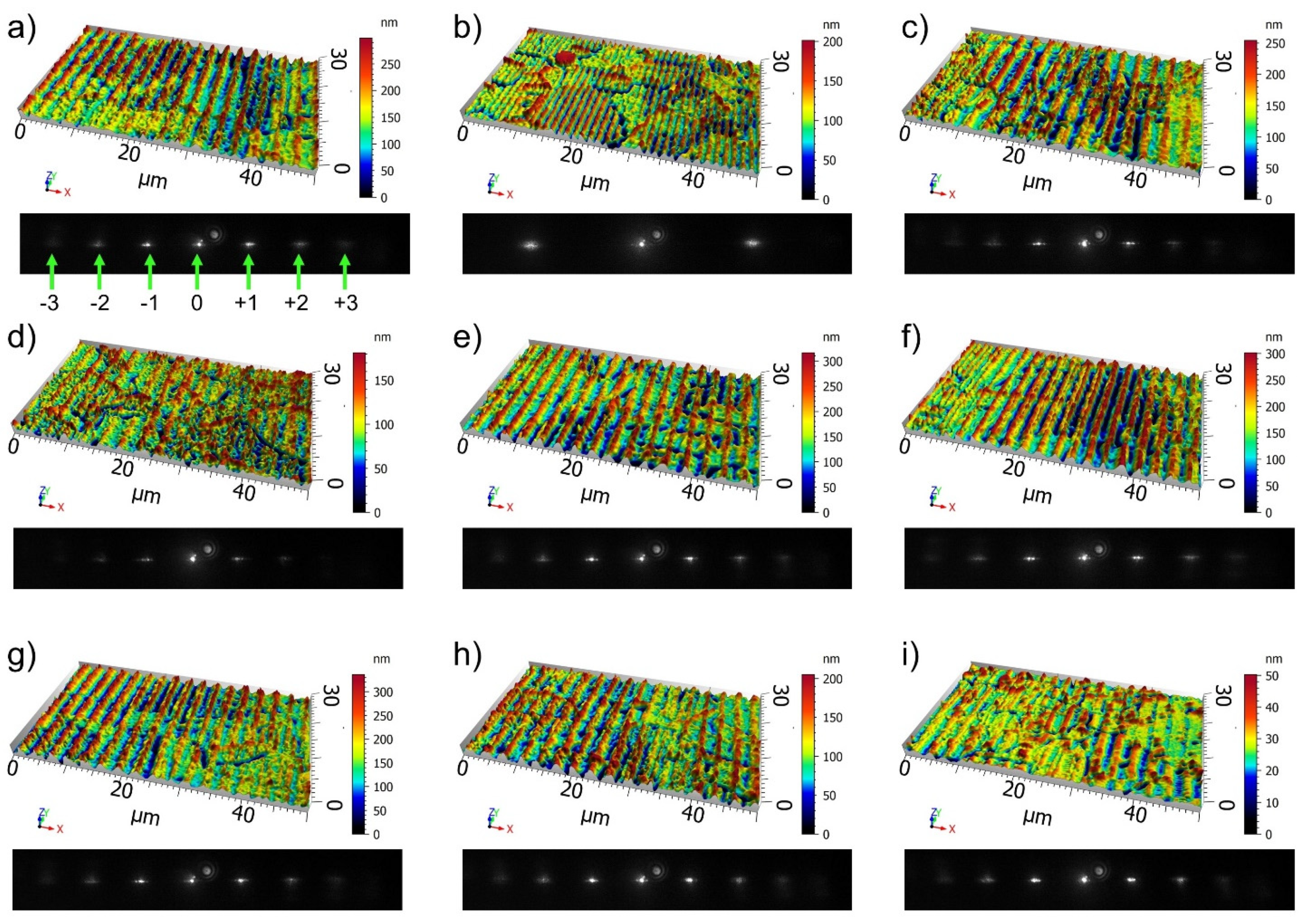
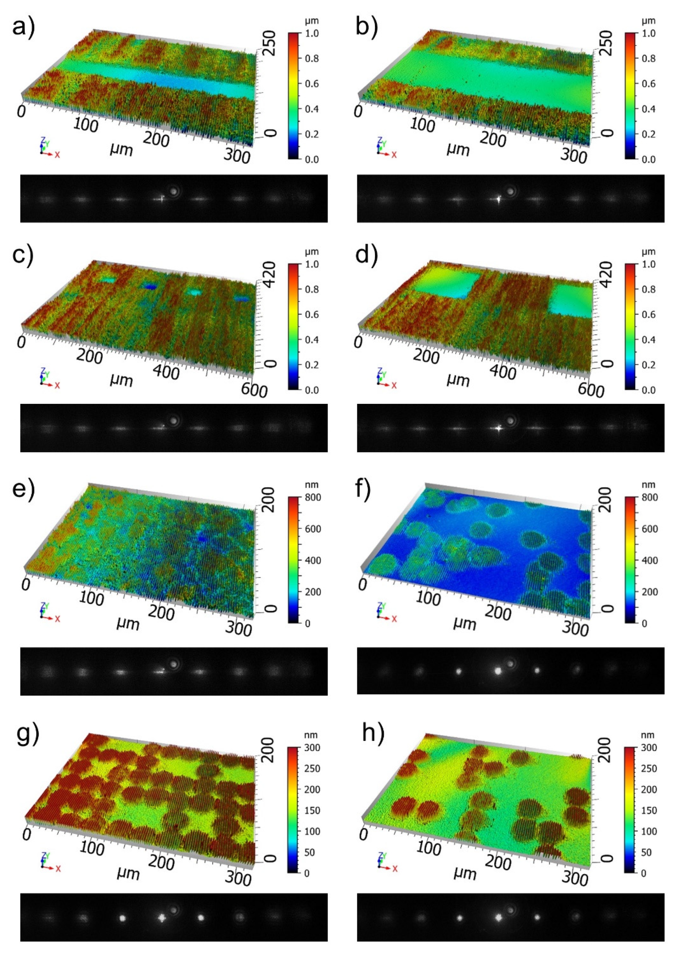
3. Results and Discussion

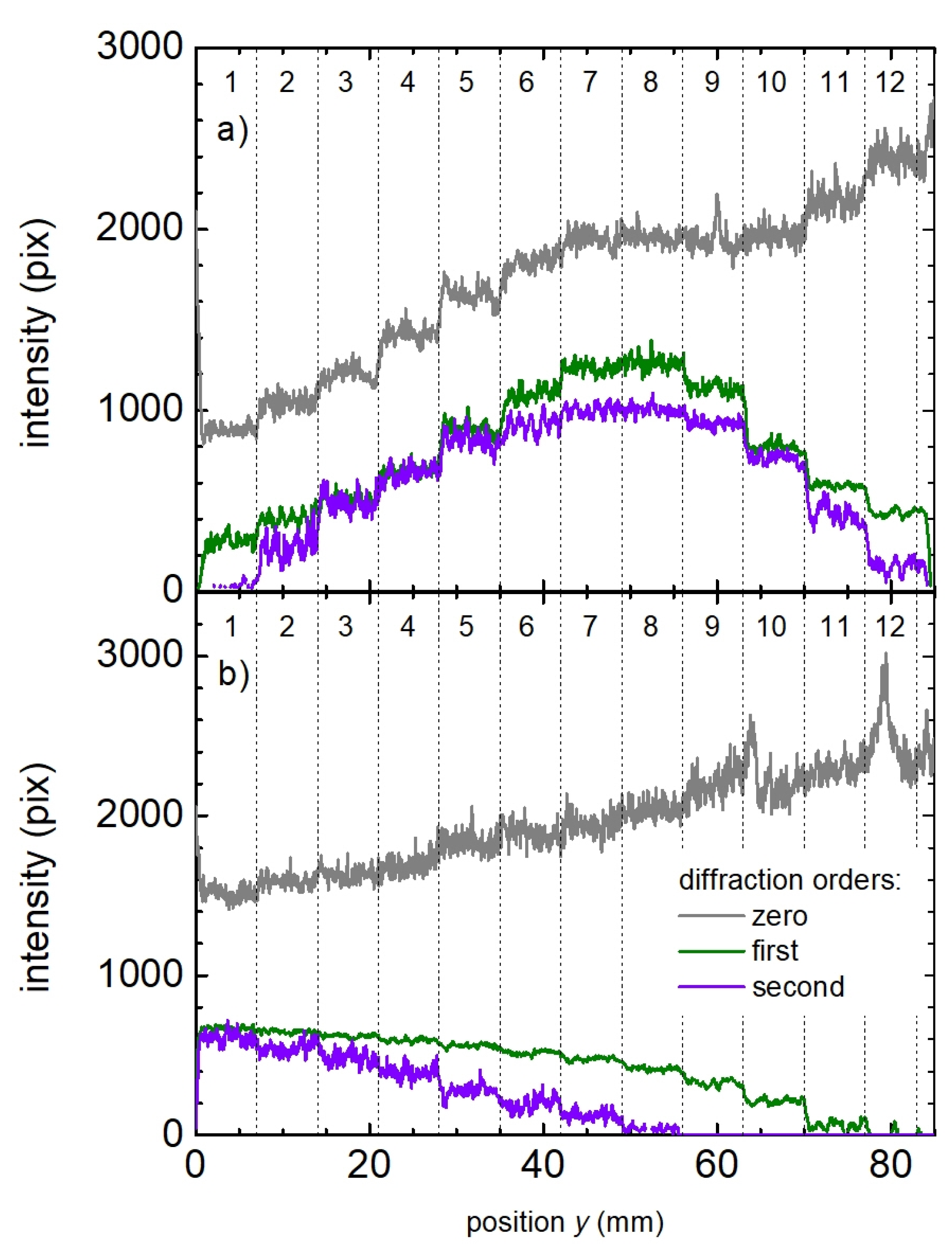
3.1. Morphology of Structured Surfaces and Associated Diffraction Patterns

Figure 3 and Figure 4 show selected confocal microscopy images of different samples with the corresponding image captured off-line with the monitoring system to visualize the impact of the introduced errors in the final topography and collected diffraction patterns. The reference texture, shown in Figure 3a, features a homogeneous line-like texture with a mean structure height of 212 nm and a calculated spatial period of 3.0 µm derived from a Fourier analysis of the topography. The CCD image features in total seven diffraction orders, as labeled in the image. Figure 3b,c correspond to the structured fields with spatial periods of 1.3 µm and 3.2 µm, respectively, on sample A. Here, it can be seen in the CCD images that the diffraction peaks are significantly shifted. In the case of Λ = 1.3 µm, only the first-order modes are visible, and they have shifted away from the center. On the contrary, in the pattern corresponding to Λ = 3.2 µm, the diffraction orders are closer to the center. The topography images of Figure 3d–f were taken from sample B, which was structured at different focus positions zf (d: zf = +300 µm, e: zf = +30 µm, f: zf = −300 µm). For the case of a slight focus shift of 30 µm, significant changes in neither the topography nor in the CCD image relative to the reference texture (Figure 3a) were observed. However, for the maximum and minimum focus shifts studied in this work, a noticeable increase and then decrease, respectively, in the spatial period was observed when analyzing the topography. These fluctuations in the spatial period as function of the focus position were also observed as a shift of the diffraction peaks positions in the CCD images and will be analyzed in the next section. The third row of Figure 3 shows results corresponding to sample C, in which the laser fluence was varied (g: 0.75 J/cm2, h: 0.63 J/cm2, i: 0.22 J/cm2). The topography images reveal a decrease in the structure height as the fluence decreases; however, the diffraction patterns in the CCD images do not show a significant variation.
Figure 4 displays some examples of samples D, E, F, and G, in which areas were left unstructured, or some pulses were not fired at random positions. In the fields shown in Figure 4a,b, stripes from sample E were intentionally left unpatterned, with a width of 42 µm and 98 µm, respectively. The CCD images show, in both cases, the complete set of characteristic diffraction peaks with a higher spreading of the intensities, mainly in the horizontal direction, compared to the reference texture. In the case of Figure 4b, the zero order has a higher intensity than in the CCD image of Figure 4a. Similarly, in the topographies of Figure 4c (sample E) and 4d (sample D), square areas with edge lengths of 19.8 µm and 210 µm, respectively, were not structured. The patterns in the CCD images are similar, although for the sample with larger flat squares (Figure 4d), the intensity of the zero order is significantly higher than in the case for the smaller square (Figure 4c). In Figure 4e,f, the topographies of sample F with an error probability of 20% and 95%, respectively, are presented. On the surface with the highest error probability, i.e., less effectively structured area, the high-order modes are less intense, whereas the zero-order intensity is higher. In the bottom row of Figure 4, the resulting textures on sample G patterned with an error probability of 20% (Figure 4g) and 80% (Figure 4h) are displayed. In this case, the CCD image of Figure 4g shows a higher intensity of the higher orders than for the case shown in Figure 4h although the intensity of the zero order is higher for the diffraction pattern in Figure 4h.

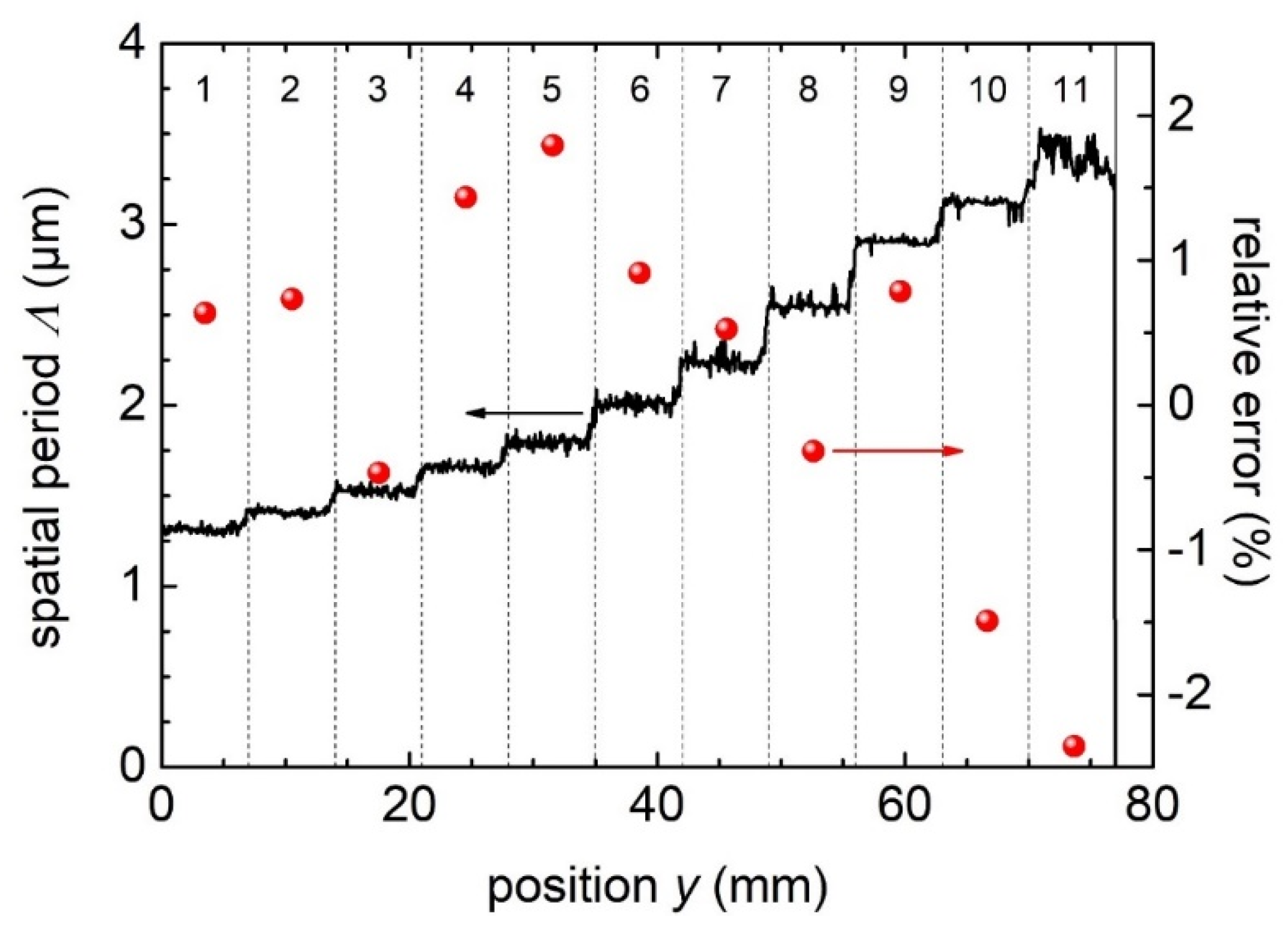
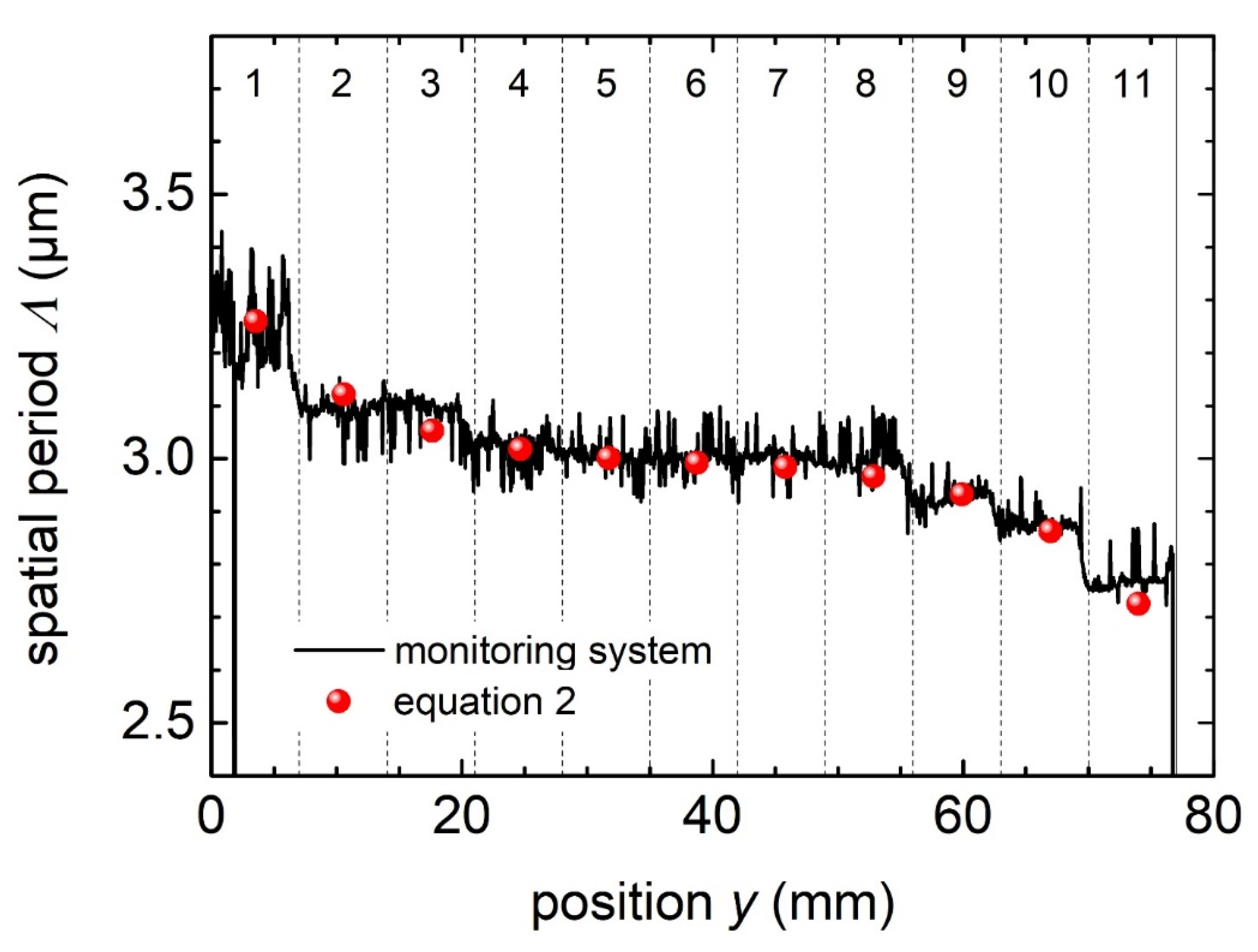
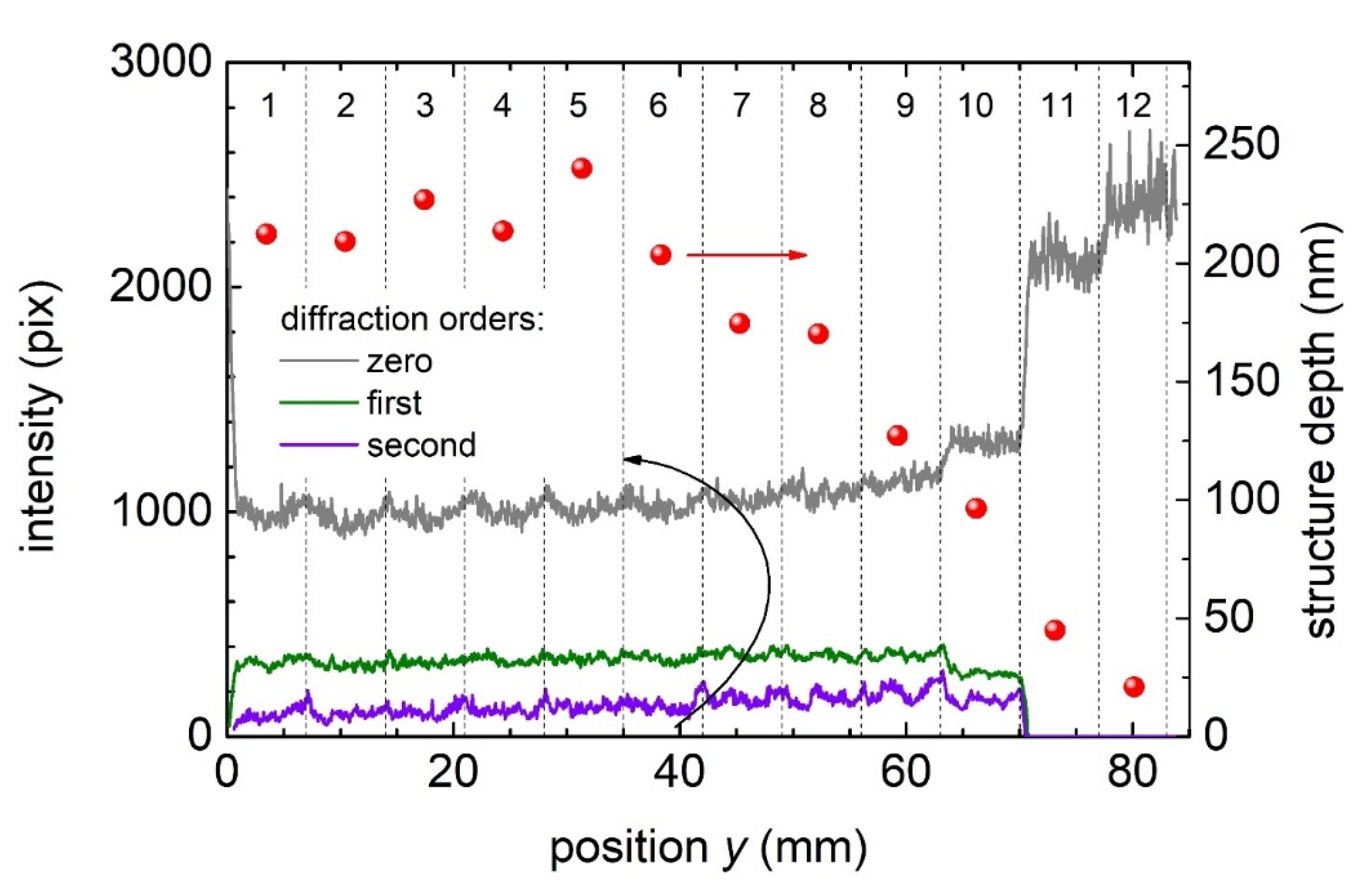
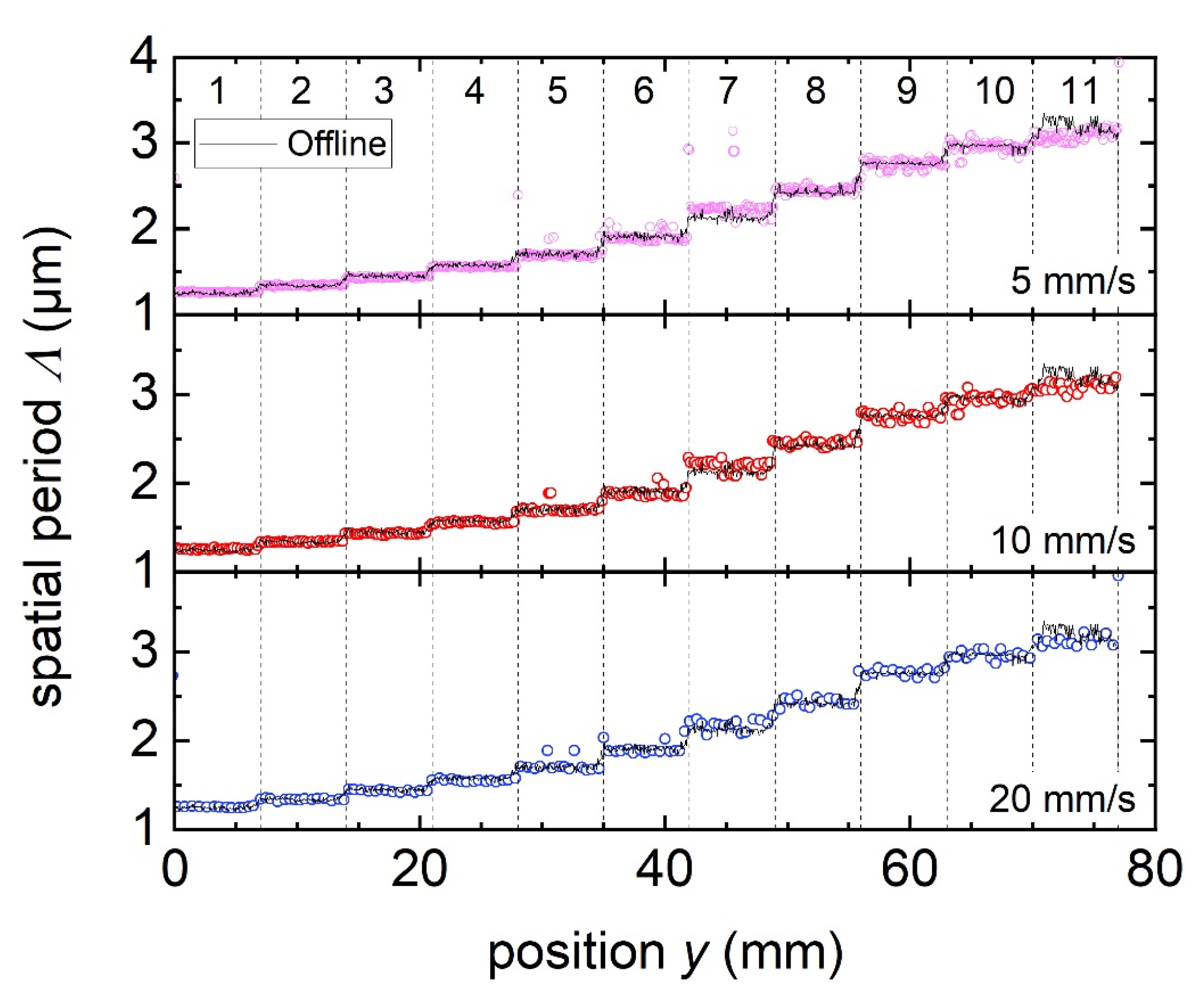
3.2. Off-Line Evaluation

The first DLIP parameter that was tested with the monitoring system was the texture spatial period, which can be directly correlated to the position of the diffraction orders in the CCD images according to the grating equation. In previous work, ray-tracing simulations were performed to establish the equivalency between the spatial period and the distance from the center of the CCD sensor [31]. In the present study, the above-mentioned equivalency was used, and to avoid offsets, a calibration was performed by measuring the topography of the reference texture with confocal microscopy.
The line in Figure 5 represents the extracted spatial period from the CCD images of sample A as a function of the position y. The average spatial period taken from topographical measurements was determined as well, showing a very good match between both methods with a relative error below 2.5% (Figure 5, red symbols). The numbering labels at the top of Figure 5 correspond to the field number in the sample. The source of error for the accurate determination of the spatial period is a combination of optical aberrations from the lenses, the projection of the orders onto the flat CCD sensor, stray light, internal reflections, and electrical noise. All of this results in diffuse and distorted diffraction orders in the collected images (see, for example, the CCD images in Figure 3 and Figure 4).
During a DLIP process, it is critical not only to ensure that the surface under treatment lies within the interference volume outlined by the overlapping beams but also that the focus position, i.e., working distance between the converging lens of the DLIP optics and surface, is constant for optimum texture quality and reproducibility. Depending on the laser beam characteristics, variations of 100–200 µm in the focus distance can yield fluctuations of the spatial period of a few hundred nanometers, ultimately deteriorating the texture uniformity. To test whether the monitoring system is able to detect changes in the topography upon deviations of the focus position, sample B was structured with 11 fields with varying focus distances (see Table 1 for details). Note that field number 6 corresponds to the reference structure fabricated at the optimum focus position. As observed in Figure 3d–f, shifts in the focus positions can induce changes in the spatial period. Therefore, in Figure 6, the extracted period from the analyzed CCD images as a function of position y in the sample is shown (black line). As indicated, field number 6, which corresponds to the reference texture, has a spatial period of 3.0 µm. As the working distance is decreased (fields 1–5; see top labels in Figure 6), the period increased, whereas the opposite is true when the DLIP optics is displaced away from the sample (fields 7–11). It can be observed that for fields number 3 and 9, a deviation in the spatial period of approximately 100 nm and −100 nm, respectively, was measured, implying that the system can detect variations in the focus position of at least ±70 µm from the optimum.
The change in the spatial period as a function of the focus position can be modeled using Equation (2) if the laser quality factor M2 and beam divergence angle Θ are known [35]:
Λ = λ 2   s i n a r c t a n z 0 z f + z 0 t a n α ,
where zf is the deviation from the optimum focus position (zf > 0 if the working distance is reduced), and z0 = λM2/πΘ2. Assuming a quality factor M2 = 1.3, as provided by the manufacturer, the divergence can be fitted with the data shown in Figure 6, yielding Θ = 8 mrad. Therefore, the method allows not only to detect fluctuations of the focus positions but also a methodology to extract the divergence (or quality factor if the divergence is given) of the beam from the measured data.
The laser power might also fluctuate during the processing of a surface, which can modify the ablation rate and thus produce deeper or shallower textures with degraded overall uniformity, as observed in Figure 3g–i. As shown in Table 1, in sample C 12 fields with varying laser fluence were produced. Figure 7 shows the mean structure depth (symbols) obtained from the confocal microscopy images sorted with the number of fields (top labels in Figure 7). It can thus be observed that for this process, when the fluence lies in the range 0.66–0.75 J/cm2 (fields 1–6), the structure depth oscillates around 220 nm ± 30 nm. However, when the fluence drops below 0.66 J/cm2, the depth decreases as well. Figure 7 shows that the intensities of the first and second diffraction orders as a function of the position y in the sample are essentially oscillating around a constant value for fields 1–8. For the zero-order intensity, the signal is constant up to the position corresponding to the field number 9 (with a fluence of 0.48 J/cm2), where its intensity starts to increase. For fields number 11 and 12, which have a very low structure depth of 48 nm and 21 nm, respectively, the first and second orders showed a clear decrease in the signal, accompanied by a steep increase in the zero-order intensity. The overall observed behavior of the diffraction orders as function of the structure depth seems not to correspond with the trends expected from the classical equations for the diffraction efficiency of sinusoidal diffraction gratings [28]. In addition, the measured intensities cannot be unequivocally correlated to the structure depths, let alone to the laser fluence. These results suggest that the algorithm implemented to detect the intensities of the diffraction orders based on calculating the area circumscribed by binary pixels associated with each order is not effective for this purpose. An improved version of the algorithm based on calculating the grayscale values of the pixels associated with each order is currently under evaluation.
Next, the monitoring system’s ability to detect missing lines, squares, or even individual spots was evaluated. To this end, the diffraction patterns corresponding to samples D–G were collected with the CCD camera, and the intensity of the diffraction peaks was quantified. As described in Table 1, samples D and E were fabricated using a patterning strategy that intentionally leaves line- and square-shaped untreated areas on the surface. The main difference between these samples is that in sample E, the unpatterned areas had smaller dimensions (see Table 1). Figure 8a,b show the intensity signals of the diffraction peaks corresponding to samples D and E, respectively. In both cases, the signal belonging to the zero diffraction order is characterized by a train of pulses with varying intensities. Whereas in sample E, some sharp valleys in the intensity of the first and hardly second diffraction orders are evident, for sample D, the intensities of the higher orders are noisy and oscillate around constant values. The pulses in the signal for the zero-order intensity and the valleys for the high-orders signals can be directly correlated to the presence of the unstructured and flat areas, which increase the specular reflection (zero-order peak) towards the CCD camera. As seen in the signal for sample D (Figure 8a), the first ten pulses correspond to the linear unstructured gaps, whereas the following nine pulses can be associated with the nine unpatterned squares. However, the signal for the zero order collected for sample E presents nine pulses with increasing intensity followed by a second train of pulses consisting of eight pulses. Therefore, the system was not able to detect the line gaps with widths of 7 µm and 14 µm or the squared areas with edge lengths of 30 µm and below, imposing a detectability limit for the system.
Finally, the textured samples in which a random distribution of missing spots was deliberately allowed were also characterized by the monitoring system. Figure 9 shows the signals corresponding to the zero, first, and second orders of sample F (a) and sample G (b). In sample F, the signals of all the diffraction orders increase as the amount of introduced errors increases (increasing position y) up to the position at 45 mm, corresponding to field number 7, where the signals reach their maxima. This counter-intuitive behavior can be explained by the fact that as the error probability increases, the texture homogeneity degrades, making the diffraction peaks broader (see Figure 4e). Because the algorithm converts the calculated area of the diffraction peaks into the intensities in Figure 9, less-defined and broader peaks tended to cause higher reconstructed intensities. When the number of missing pulses was high enough, a condition which, in these experiments, was reached for field number 9, the texture became so inhomogeneous that the diffraction efficiency began to decrease. Therefore, from the fields 9 to 12, the signals of the first and second order decreased significantly, whereas the zero-order intensity increased.
In the chosen patterning strategy for sample G, the overlapping of adjacent pulses was excluded. The resulting average structure depth was 203 nm, i.e., 63% lower than in the reference texture. The diffraction orders signals corresponding to this sample, shown in Figure 9b, presented a clear trend: while the intensity of the zero order increased almost linearly with the increasing number of missing structured spots, the higher orders’ intensity decreased accordingly. This behavior can be simply attributed to the fact that the less structured area the sample has, the lower the overall diffraction efficiency of the illuminated area will be. It is worth mentioning that in contrast to sample F, in sample G, the area of flat unstructured surface increases linearly with the error probability.
With the information derived from the monitoring results, different scenarios corresponding to specific structuring processes can be devised, where the presented approach can be useful. As the variations of fluence could not be successfully monitored with the current system, an additional sensor, e.g., a beam-splitter combined with a photodiode, could be integrated to monitor this variable. As a first possible scenario, a DLIP process with a constant user-defined spatial period and overlapping pulses strategy was analyzed. The signal of the spatial period can thus accurately provide the real spatial period of the textures, and variations thereof can be interpreted as fluctuations in the focus position, as was the case of sample B and shown in Figure 6. Increasing intensities of all the diffraction orders can be ascribed to the broadening of the diffraction peaks. According to the results of Figure 9a, it can be assumed that a considerable amount of discrete and randomly located pulses were not fired. If the amount of missing pulses is considerably high, the intensity of the first and second orders would be low. Furthermore, if sharp peaks are detected in the zero-order signal, then it can be assumed that unstructured areas are present.
A second scenario could be created in which the pulses are fired adjacent to one another (no overlap). The rest of the conditions would remain equal, as in the first example. Here, an increase in the zero-order intensity accompanied by a decrease in the other orders would imply unstructured spots due to missing pulses, as displayed in Figure 9b.
Finally, a third hypothetical process would be DLIP patterning of surfaces with different spatial periods to achieve complex topographies for decorative applications, for instance, ref. [36]. In such case, the determination of the user-defined spatial periods can be accurately supervised by the algorithm, and fluctuations around the set values can be detected. Depending on the used strategy (overlapping or adjacent pulses), the signal intensities of the diffraction orders can reveal the presence of texture defects, as described above.

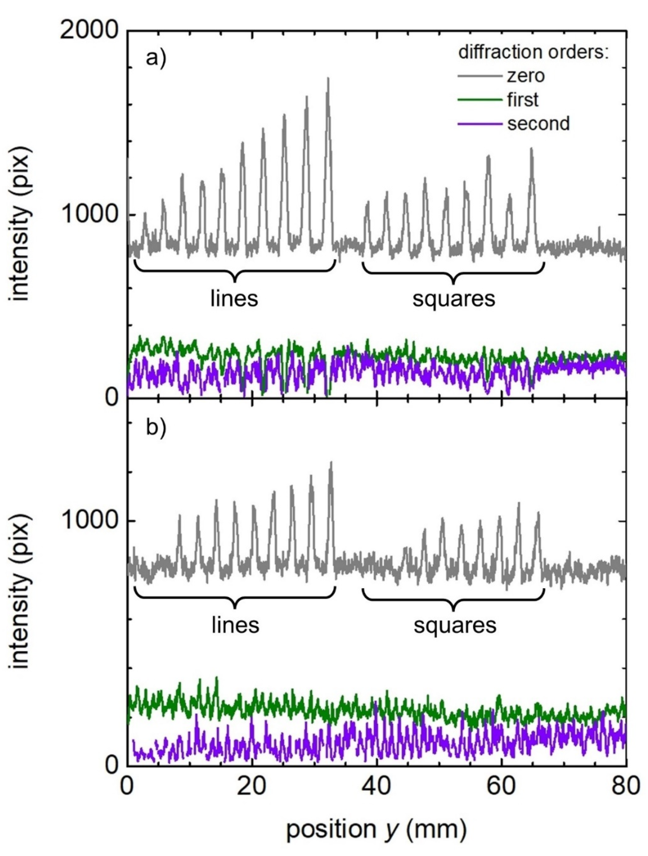
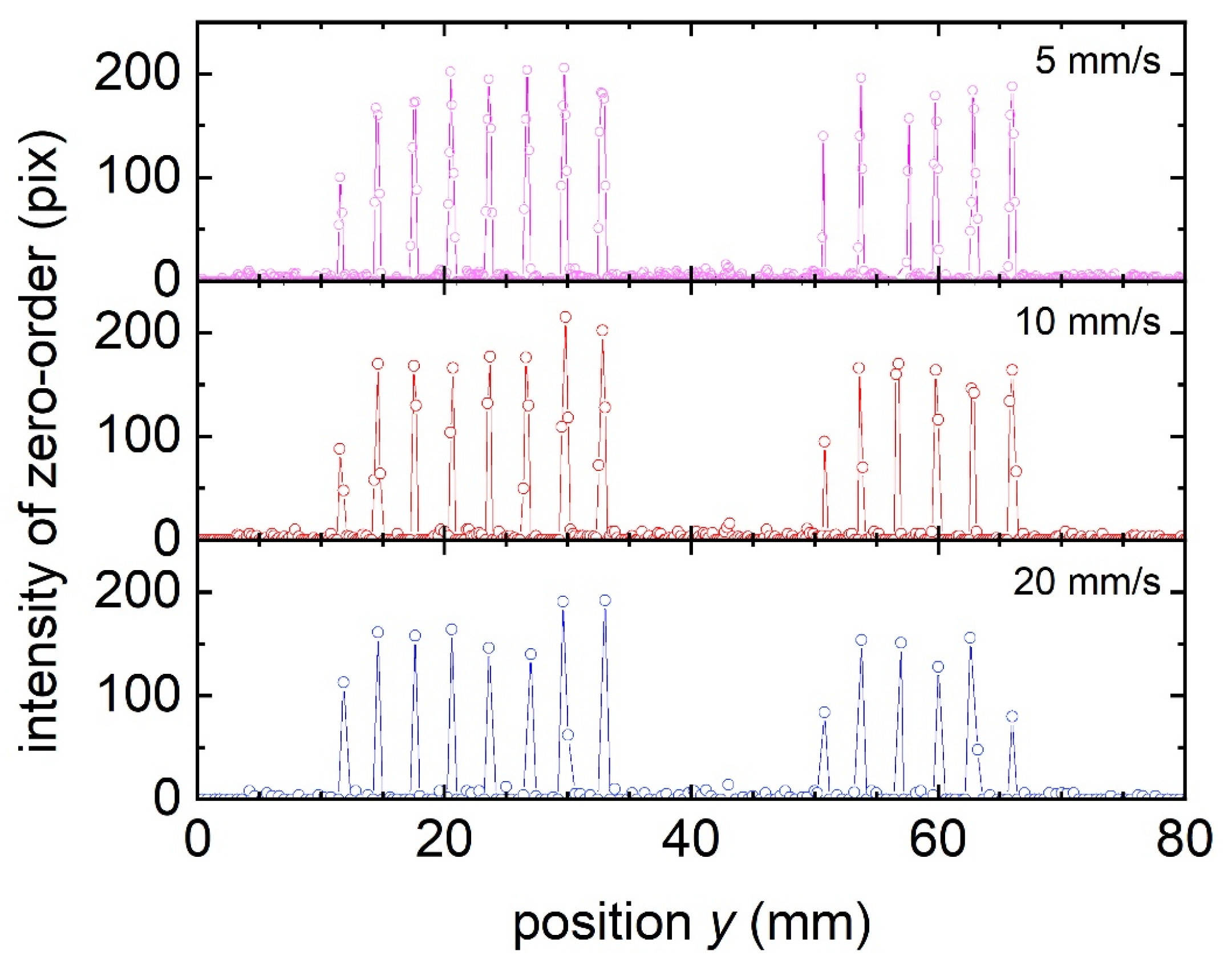
3.3. Real-Time Evaluation

The monitoring system was also evaluated in real-time; i.e., the algorithm was modified to generate the resulting data, while the sample was scanned under the monitoring unit. The axis speed was set at 5 mm/s, 10 mm/s, and 20 mm/s, whereas the camera frame rate was adjusted to a value of 50 fps, implying a spatial step size of 100 µm, 200 µm, and 400 µm, respectively, between frames. It is worth mentioning that 50 fps is the maximum value achievable at the selected field of view (1256 × 550 pixels). On the other hand, the algorithm reduces the camera frame rate if it needs more time to perform the calculation depending on the complexity of the processed image, which increases the spatial step size accordingly. Figure 10 shows the spatial period extracted from sample A for the three speeds labeled in the plot (symbols), superimposed with the previously off-line measured spatial period (black line). It can be observed that as the axis speed is increased, the measured spatial period is sampled with fewer datapoints. Although a few data outliers can be detected, the measurements in real time match very well those from the off-line characterization.
Finally, to test the resolution of the real-time monitoring system, the sample E was measured at three different axis speeds, namely 5, 10, and 20 mm/s. The measured intensity of the zero diffraction order as function of the sample position is shown in Figure 11. Notice that the light intensity of the laser diode was reduced with the polarizer to obtain fewer illuminated pixels in the captured images and speed up the calculation. From the figure, it can be seen that eight unpatterned gaps and six unpatterned squares were detected. Thus, the detection limit can be set at 42 µm for unstructured gaps and 60 µm for missing patterned squares. Recalling the measurement shown in Figure 8b, with the off-line procedure, nine missing lines and eight missing squares could be detected, and therefore, the real-time monitoring yielded a reduced detection resolution. It can be observed that the employed sampling rate for the highest used speed of 20 mm/s provides just one datapoint per missing line or square. This suggests that for the used approach and settings, further increasing the axis speed would imply an insufficient spatial resolution and an increased probability of skipping structuring defects. The real-time experiments, as those shown in Figure 10 and Figure 11, were performed three times, and similar characteristics and identical detection limits were obtained.

4. Conclusions

In summary, the presented set of experiments was successfully employed to test and validate a compact monitoring system useful for tracking the reproducibility of laser-microtexturing processes in both off-line and real-time operation. The method allowed for an accurate estimation of the patterned spatial period in a minimum range from 1.3 µm to 3.3 µm and with a precision of at least 100 nm. Focus shifts can be identified by tracking the positions of the first-order diffraction peaks, yielding a sensitivity of approximately 70 µm in the focus position. Missing lines during the laser texturing can be identified off-line as long as they have a width of at least 28 µm; however, in real-time monitoring, the detectivity limit was increased to 42 µm. It is suggested that a higher sensitivity to detect texture height variations can be obtained if the intensity of the peaks is calculated from the integral of the grayscale values instead of using the contour area. An algorithm that uses this approach is currently under evaluation.

Author Contributions

Conceptualization, M.S. and A.F.L.; methodology, S.T.-W. and N.S.; software, S.T.-W., N.S. and B.V.; validation, M.S. and N.S.; formal analysis, M.S., N.S. and B.V.; investigation, M.S. and N.S.; resources, A.F.L.; data curation, M.S., S.T.-W. and N.S.; writing—original draft preparation, M.S.; writing—review and editing, N.S. and A.F.L.; visualization, M.S.; supervision, M.S. and A.F.L.; project administration, M.S.; funding acquisition, A.F.L. All authors have read and agreed to the published version of the manuscript.

Funding

This work was carried out in the framework of the Reinhart–Koselleck project (323477257), which has received funding from the German Research Foundation (German: Deutsche Forschungsgemeinschaft DFG). This project has also received funding from the European Union’s Horizon 2020 research and innovation programme under Grant Agreement No. 825132. It is an initiative of the Photonics Public Private Partnership www.photonics21.org. This work reflects only the author’s view, and the EU is not responsible for any use that may be made of the presented information. The work of A.F.L. is also supported by the German Research Foundation (DFG) under Excellence Initiative program by the German federal and state government to promote top-level research at German universities.

Data Availability Statement

The data presented in this study are available on request from the corresponding author.

Conflicts of Interest

The authors declare no conflict of interest.

References

  1. Phillips, K.C.; Gandhi, H.H.; Mazur, E.; Sundaram, S.K. Ultrafast Laser Processing of Materials: A Review. Adv. Opt. Photon. 2015, 7, 684–712. [Google Scholar] [CrossRef]
  2. Malinauskas, M.; Žukauskas, A.; Hasegawa, S.; Hayasaki, Y.; Mizeikis, V.; Buividas, R.; Juodkazis, S. Ultrafast Laser Processing of Materials: From Science to Industry. Light Sci. Appl. 2016, 5, e16133. [Google Scholar] [CrossRef] [PubMed] [Green Version]
  3. Stratakis, E.; Bonse, J.; Heitz, J.; Siegel, J.; Tsibidis, G.D.; Skoulas, E.; Papadopoulos, A.; Mimidis, A.; Joel, A.C.; Comanns, P.; et al. Laser Engineering of Biomimetic Surfaces. Mater. Sci. Eng. R 2020, 141, 100562. [Google Scholar] [CrossRef]
  4. Vorobyev, A.Y.; Guo, C. Multifunctional Surfaces Produced by Femtosecond Laser Pulses. J. Appl. Phys. 2015, 117, 033103. [Google Scholar] [CrossRef] [Green Version]
  5. Bonse, J.; Höhm, S.; Kirner, S.V.; Rosenfeld, A.; Krüger, J. Laser-Induced Periodic Surface Structures— A Scientific Evergreen. IEEE J. Sel. Top. Quant. 2017, 23, 9000615. [Google Scholar] [CrossRef]
  6. El-Kady, M.F.; Kaner, R.B. Direct Laser Writing of Graphene Electronics. ACS Nano 2014, 8, 8725–8729. [Google Scholar] [CrossRef] [PubMed]
  7. Bonse, J. Quo Vadis LIPSS?—Recent and Future Trends on Laser-Induced Periodic Surface Structures. Nanomaterials 2020, 10, 1950. [Google Scholar] [CrossRef]
  8. Lasagni, A.F. Laser Interference Patterning Methods: Possibilities for High-Throughput Fabrication of Periodic Surface Patterns. Adv. Opt. Tech. 2017, 6, 265–275. [Google Scholar] [CrossRef]
  9. Voisiat, B.; Zwahr, C.; Lasagni, A.F. Growth of Regular Micro-Pillar Arrays on Steel by Polarization-Controlled Laser Interference Patterning. Appl. Surf. Sci. 2019, 471, 1065–1071. [Google Scholar] [CrossRef]
  10. Indrišiūnas, S.; Voisiat, B.; Gedvilas, M.; Račiukaitis, G. New Opportunities for Custom-Shape Patterning Using Polarization Control in Confocal Laser Beam Interference Setup. J. Laser. Appl. 2017, 29, 011501. [Google Scholar] [CrossRef]
  11. Mulko, L.; Soldera, M.; Lasagni, A.F. Structuring and Functionalization of Non-Metallic Materials Using Direct Laser Interference Patterning: A Review. Nanophotonics 2022, 11, 203–240. [Google Scholar] [CrossRef]
  12. Tran, D.V.; Lam, Y.C.; Wong, B.S.; Zheng, H.Y.; Hardt, D.E. Quantification of Thermal Energy Deposited in Silicon by Multiple Femtosecond Laser Pulses. Opt. Express 2006, 14, 9261–9268. [Google Scholar] [CrossRef] [PubMed]
  13. Tran, D.V.; Lam, Y.C.; Zheng, H.Y.; Wong, B.S.; Hardt, D.E. Direct Observation of the Temperature Field during Ablation of Materials by Multiple Femtosecond Laser Pulses. Appl. Surf. Sci. 2007, 253, 7290–7294. [Google Scholar] [CrossRef]
  14. Schröder, N.; Vergara, G.; Voisat, B.; Lasagni, A.F. Monitoring the Heat Accumulation during Fabrication of Surface Micropatterns on Metallic Surfaces Using Direct Laser Interference Patterning. J. Laser Micro Nanoeng. 2020, 15, 150–157. [Google Scholar]
  15. Schröder, N.; Teutoburg-Weiss, S.; Vergara, G.; Lasagni, A.F. New Approach for Monitoring a Direct Laser Interference Patterning Process Using a Combination of an Infrared Camera and a Diffraction Measurement System. J. Laser Micro Nanoeng. 2021, 16, 131–137. [Google Scholar]
  16. Langeheinecke, H.J.; Tutunjian, S.; Soldera, M.; Wegner, W.; Lasagni, A.F. Analyzing the Electromagnetic Radiations Emitted during a Laser-Based Surface Pre-Treatment Process for Aluminium Using Diode Sensors as an Approach for High-Resolution Online Monitoring. J. Laser Micro Nanoeng. 2022, 17, 141–149. [Google Scholar] [CrossRef]
  17. Stauter, C.; Gérard, P.; Fontaine, J.; Engel, T. Laser Ablation Acoustical Monitoring. Appl. Surf. Sci. 1997, 109–110, 174–178. [Google Scholar] [CrossRef]
  18. Steege, T.; Alamri, S.; Lasagni, A.F.; Kunze, T. Detection and Analysis of Photo-Acoustic Emission in Direct Laser Interference Patterning. Sci. Rep. 2021, 11, 14540. [Google Scholar] [CrossRef]
  19. Rodríguez, F.; Cotto, I.; Dasilva, S.; Rey, P.; der Straeten, K.V. Speckle Characterization of Surface Roughness Obtained by Laser Texturing. Procedia Manuf. 2017, 13, 519–525. [Google Scholar] [CrossRef]
  20. Li, L.; Haggans, C.W. Convergence of the Coupled-Wave Method for Metallic Lamellar Diffraction Gratings. J. Opt. Soc. Am. A 1993, 10, 1184–1189. [Google Scholar] [CrossRef]
  21. Moharam, M.G.; Gaylord, T.K. Rigorous Coupled-Wave Analysis of Grating Diffraction—E-Mode Polarization and Losses. J. Opt. Soc. Am. 1983, 73, 451–455. [Google Scholar] [CrossRef]
  22. Lalanne, P.; Morris, G.M. Highly Improved Convergence of the Coupled-Wave Method for TM Polarization. J. Opt. Soc. Am. A 1996, 13, 779–784. [Google Scholar] [CrossRef]
  23. Knop, K. Rigorous Diffraction Theory for Transmission Phase Gratings with Deep Rectangular Grooves. J. Opt. Soc. Am. 1978, 68, 1206–1210. [Google Scholar] [CrossRef]
  24. Oh, C.; Escuti, M.J. Numerical Analysis of Polarization Gratings Using the Finite-Difference Time-Domain Method. Phys. Rev. A 2007, 76, 043815. [Google Scholar] [CrossRef] [Green Version]
  25. Ichikawa, H. Electromagnetic Analysis of Diffraction Gratings by the Finite-Difference Time-Domain Method. J. Opt. Soc. Am. A 1998, 15, 152–157. [Google Scholar] [CrossRef]
  26. Delort, T.; Maystre, D. Finite-Element Method for Gratings. J. Opt. Soc. Am. A 1993, 10, 2592–2601. [Google Scholar] [CrossRef]
  27. Bao, G.; Chen, Z.; Wu, H. Adaptive Finite-Element Method for Diffraction Gratings. J. Opt. Soc. Am. A 2005, 22, 1106–1114. [Google Scholar] [CrossRef]
  28. Harvey, J.E.; Pfisterer, R.N. Understanding Diffraction Grating Behavior: Including Conical Diffraction and Rayleigh Anomalies from Transmission Gratings. Opt. Eng. 2019, 58, 087105. [Google Scholar] [CrossRef]
  29. Harvey, J.E.; Pfisterer, R.N. Understanding Diffraction Grating Behavior, Part II: Parametric Diffraction Efficiency of Sinusoidal Reflection (Holographic) Gratings. Opt. Eng. 2020, 59, 017103. [Google Scholar] [CrossRef]
  30. Michalek, A.; Jwad, T.; Penchev, P.; See, T.L.; Dimov, S. Inline LIPSS Monitoring Method Employing Light Diffraction. J. Micro Nanomanuf. 2020, 8, 011002. [Google Scholar] [CrossRef] [Green Version]
  31. Teutoburg-Weiss, S.; Voisiat, B.; Soldera, M.; Lasagni, A.F. Development of a Monitoring Strategy for Laser-Textured Metallic Surfaces Using a Diffractive Approach. Materials 2020, 13, 53. [Google Scholar] [CrossRef] [PubMed] [Green Version]
  32. Schröder, N.; Fischer, C.; Soldera, M.; Bouchard, F.; Voisiat, B.; Lasagni, A.F. Approach for Monitoring the Topography of Laser-Induced Periodic Surface Structures Using a Diffraction-Based Measurement Method. Mater. Lett. 2022, 324, 132794. [Google Scholar] [CrossRef]
  33. Fu, Y.; Soldera, M.; Wang, W.; Voisiat, B.; Lasagni, A.F. Picosecond Laser Interference Patterning of Periodical Micro-Architectures on Metallic Molds for Hot Embossing. Materials 2019, 12, 3409. [Google Scholar] [CrossRef] [PubMed] [Green Version]
  34. Culjak, I.; Abram, D.; Pribanic, T.; Dzapo, H.; Cifrek, M. A Brief Introduction to OpenCV. In Proceedings of the 2012 35th International Convention MIPRO, Opatija, Croatia, 21–25 May 2012; IEEE: New York, NY, USA, 2012; pp. 1725–1730. [Google Scholar]
  35. Gärtner, A. Development of Methods for the Processing of Three Dimensional Surfaces by Means of Direct Laser Interference Patterning; Technische Universität Dresden: Dresden, Germany, 2015. [Google Scholar]
  36. Voisiat, B.; Wang, W.; Holzhey, M.; Lasagni, A.F. Improving the Homogeneity of Diffraction Based Colours by Fabricating Periodic Patterns with Gradient Spatial Period Using Direct Laser Interference Patterning. Sci. Rep. 2019, 9, 7801. [Google Scholar] [CrossRef] [PubMed] [Green Version]
Figure 1. Schematic setup of the (a) DLIP station used to pattern line-like structures on the stainless steel plate and (b) optical system employed to monitor the texture morphology of the different samples.
Optics 04 00014 g001
Figure 2. Schematics of the patterned steel plate (100 × 100 mm2) with the seven samples (A–G). In each sample, a different laser parameter was varied, or some areas were deliberately left unstructured by avoiding firing pulses at given positions (see Table 1 and text for details). The red color points at unstructured or partially structured areas.
Optics 04 00014 g002
Figure 3. Selected topography images from samples A–C and their corresponding diffraction patterns captured with the monitoring system. The first row shows patterned fields of sample A with varying spatial periods of (a) 3.0 µm (reference texture), (b) 1.4 µm, and (c) 3.2 µm. In the second row, different fields belonging to sample B are shown, which were structured at different focus positions with respect to the reference texture: (d) 300 µm, (e) 30 µm, and (f) −300 µm. The third row shows fields corresponding to sample C, in which the fluence was varied: (g) 0.75 J/cm2, (h) 0.63 J/cm2, and (i) 0.22 J/cm2.
Optics 04 00014 g003
Figure 4. Selected topography images from samples D–G and their corresponding diffraction patterns captured with the monitoring system. In the first row, unpatterned stripes with line widths of (a) 42 µm and (b) 98 µm are displayed. The second row shows examples of untreated squares with edge lengths of (c) 19.8 µm and (d) 210 µm. In the third and fourth rows fields, different probabilities of skipping pulses are shown: (e) 20% and (f) 95% correspond to sample F, whereas (g) 20% and (h) 80% belong to sample G.
Optics 04 00014 g004
Figure 5. Spatial period extracted from the CCD images as a function of the position in sample A (black line). The symbols stand for the relative error between the measured spatial period with the monitoring system and the spatial period extracted from topographical images.
Optics 04 00014 g005
Figure 6. Measured spatial period with the monitoring unit (black line) as a function of the position in sample B. The symbols represent the spatial period calculated with Equation (2).
Optics 04 00014 g006
Figure 7. Intensity of the diffraction peaks (lines; see legend) as a function of the position in sample C. The symbols stand for the structure depth (right axis) determined from confocal microscopy.
Optics 04 00014 g007
Figure 8. Intensity of the diffraction peaks (lines; see legend) as a function of the position in samples (a) D and (b) E.
Optics 04 00014 g008
Figure 9. Intensity of the diffraction peaks (lines; see legend) as a function of the position in samples (a) F (overlapping pulses) and (b) G (no overlap between pulses).
Optics 04 00014 g009
Figure 10. Real-time calculation of spatial period (colored symbols) on sample A at three axis speeds. The black lines correspond to the off-line results from Figure 5.
Optics 04 00014 g010
Figure 11. Real-time calculation of intensity of zero order on sample E at three axis speeds. The lines are guides to the eye.
Optics 04 00014 g011
Table 1. DLIP parameters for the fabrication of the structured samples.
Sample ASample BSample CSample DSample ESample FSample G
Field #Spatial Period (µm)Focus Deviation (mm)Fluence (J/cm2)Unpatterned Line Width (µm)Unpatterned Squares Edge (µm)Unpatterned Line Width (µm)Unpatterned Squares Edge (µm)Error prob. (%)Error prob. (%)
11.30.310.75135357700
21.40.150.7417070149.91010
31.50.070.7281401402819.82020
41.70.030.7082102104229.73030
51.80.010.6822802805639.64040
62.000.6573503507049.55050
72.3−0.010.6324204908459.46060
82.5−0.030.5354905609869.37070
92.9−0.070.48156063012679.28080
103.1−0.150.362630-14089.19090
113.3−0.310.216--15499.09595
12--0.031---108.997.597.5
Disclaimer/Publisher’s Note: The statements, opinions and data contained in all publications are solely those of the individual author(s) and contributor(s) and not of MDPI and/or the editor(s). MDPI and/or the editor(s) disclaim responsibility for any injury to people or property resulting from any ideas, methods, instructions or products referred to in the content.

