Article

A Spectroscopic Evaluation of the Generation Process of Semiconductor Nanoparticles (ZnO) by DC Arc Plasma

Graduate School of Natural Science and Technology, Shimane University, 1060 Nishikawatsu, Matsue 690-8504, Japan
*
Author to whom correspondence should be addressed.
J 2023, 6(2), 207-219; https://doi.org/10.3390/j6020016
Submission received: 28 February 2023 / Revised: 30 March 2023 / Accepted: 4 April 2023 / Published: 7 April 2023
(This article belongs to the Section Chemistry & Material Sciences)

Abstract

:
The fabrication of ZnO nanoparticles (NPs) was monitored and studied in situ by controlling the plasma parameters of the direct current (DC) arc plasma system, such as the current density and chamber pressure. The optical emission signature of nitrogen was spectroscopically studied using optical emission spectroscopy (OES) techniques, and it showed a dependency on the nitrogen concentration in the ZnO nanoparticles in relation to the output of the ZnO NPs-based homojunction light-emitting diodes (LEDs). The synthesized NPs had a good crystalline quality and hexagonal wurtzite structure, and they were characterized by X-ray diffraction (XRD) techniques and scanning electron microscope (SEM). The photoluminescence properties of the ZnO NPs and the optical and electrical parameters of the LEDs were also analyzed and correlated. The results indicate that the nitrogen dopants act as acceptors in the ZnO NPs and are favored in low plasma temperatures during fabrication. We anticipate that the results can provide an effective way to realize reliable nitrogen-doped p-type ZnO and tremendously encourage the development of low-dimensional ZnO homojunction LEDs.

1. Introduction

ZnO-based semiconductor nanoparticles have been studied for a long time for their potential in multifaceted fields, such as optoelectronics (LEDs [1], lasers [2], photodetectors [3]); photocatalysis [4,5]; chemical sensing [6]; piezoelectric devices [7]; biomarkers [8]; storage application [9,10]; and so on. ZnO, which is a wide-bandgap semiconductor (3.36 eV), has gained popularity in recent years and is sought to replace the current GaN-based LEDs due to the high exciton binding energy (60 meV) exhibited at room temperature. The main bottleneck problem for ZnO remains a challenge to the obtainment of high-quality, stable, and reproducible p-ZnO with high conductivity and mobility [11]. Intrinsically, ZnO behaves as an n-type semiconductor that arises due to native defects, such as O vacancies, Zn interstitials, and Zn anti-sites. Thus, many groups have demonstrated ZnO-based heterojunction LEDs utilizing ZnO as the n layer, which is used in conjunction with other p-type materials, such as GaN [12], SiC [13], or Si [14], as well as demonstrating the heterostructures of ZnO alloys [15,16]; however, we still lack homojunction LEDs with high stability and repeatability.
Many attempts have been made to achieve p-type conductivity using group I or group V as dopants [17]. Theoretical studies have shown that nitrogen is a good acceptor material [18]. Our group also employed nitrogen-doped ZnO NPs to fabricate homojunction LEDs [19], and we also successfully demonstrated heterojunction-based LEDs using metalorganic vapor-phase epitaxy techniques [20]. In conjunction with the film, low-dimension ZnO has been successfully inserted as an active material in LEDs [21]. ZnO thin film can be grown by various techniques, such as radio frequency sputtering [19], metalorganic vapor phase epitaxy (MOVPE) [20], molecular beam epitaxy (MBE) [1], and electrochemical deposition [22]. However, single-crystal substrates and epitaxial growth processes need stringent fabrication controls and are currently expensive. Meanwhile, the manufacture of LEDs employing nanoparticles (NPs) is affordable and scalable, and it may be performed under ambient settings.
Low-dimension ZnO has been utilized in many forms in LED operations, such as nanoparticles (NPs) and nanowires [23,24]. Low dimensions also possess a large surface-to-volume ratio, which enables facile incorporation of dopants at a high concentration, making an effective doping method for ZnO nanostructures. Low-dimension ZnO can be fabricated in many ways, such as using the sol–gel [25], hydrothermal [26], microwave [27], precipitation [28], radio frequency (RF) thermal plasma [29], and arc discharge methods [30,31], among others.
Arc discharge methods are easily scalable, and ZnO NPs can be formed by large-area uniform production. In contrast to the considerable literature on ZnO NPs formed by various processes and their characteristics, it appears that little work has been conducted on elucidating the arc discharge process while characterizing the ablation plume from which such NPs are created. Mechanisms that involve the doping process and the expansion of plasma plumes are still not well-explored using optical emission spectroscopy (OES) techniques. Previous works regarding OES do not compare the plasma properties with the nitrogen incorporation in the ZnO, and the use of ambient air or dry air may lead to some ambiguity due to the presence of unwanted gas [32,33]. Herein, we spectroscopically evaluated the fabrication of nitrogen-doped p-type ZnO nanoparticles using arc discharge equipment by varying the current density and pressure conditions. The efficient doping conditions were investigated using OES methods by using a mixture of pure gas (nitrogen + oxygen), and they were validated by fabricating LEDs using the p-type ZnO NPs. Our study not only advances the synthesis of nitrogen-doped p-type ZnO nanocrystal materials but also provides an innovative design to construct low-dimensional ZnO homojunction optoelectronic devices such as LEDs with pure UV light.

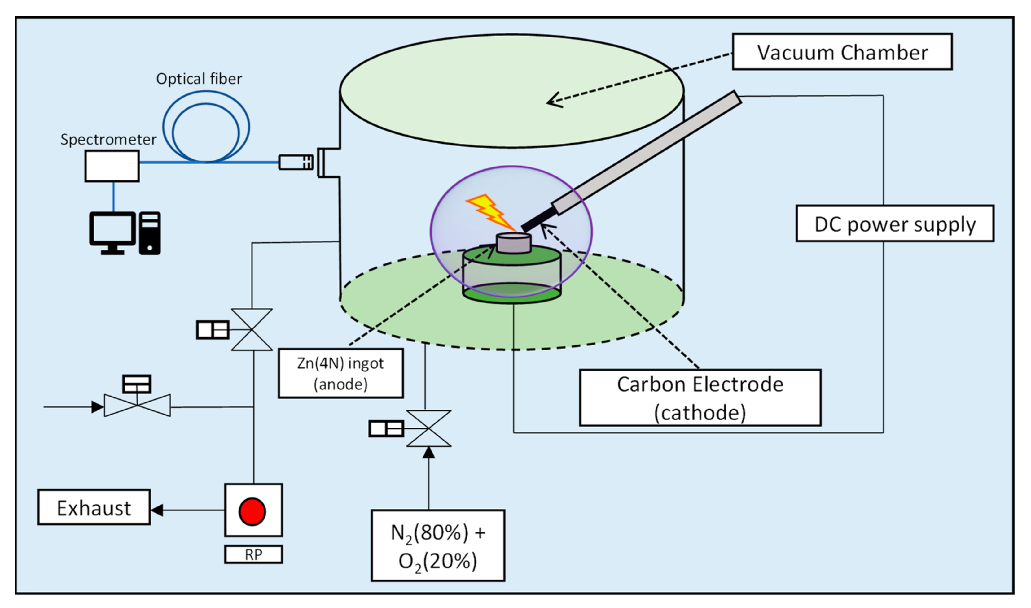
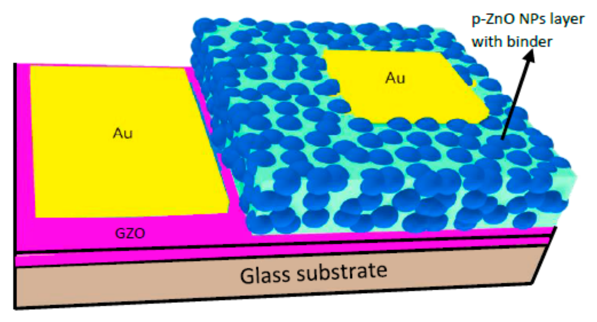
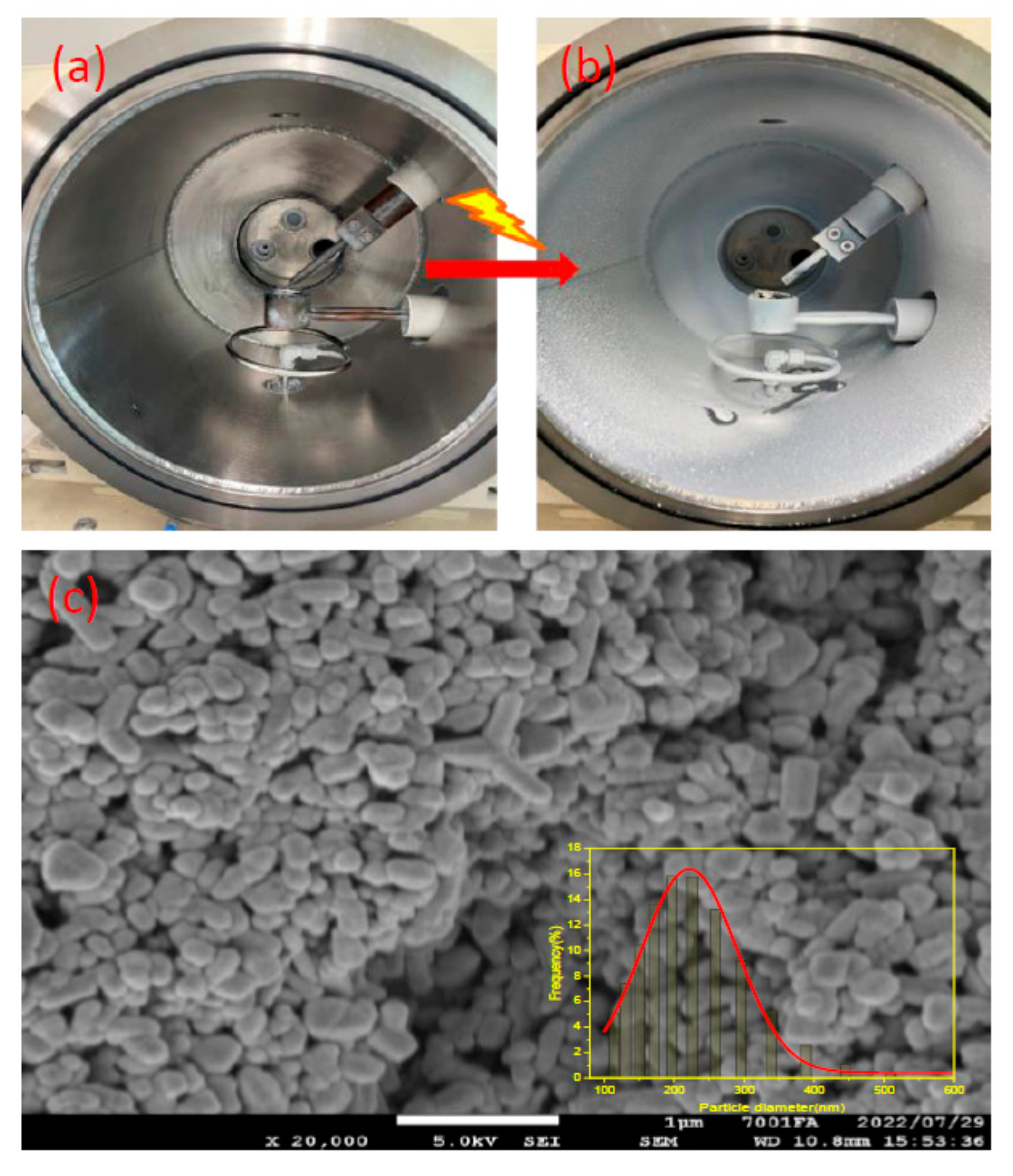
2. Materials and Methods

Nitrogen-doped p-type ZnO nanoparticles were prepared by the arc discharge apparatus (ULVAC Inc., Model No-GE-970, Chigasaki, Kanagawa, Japan), as shown in Figure 1. The details regarding the discharge process are briefly discussed [32]. Firstly, 4N zinc rods were cut into small pieces and were heated in a ceramic crucible at 600 °C to form zinc ingots. The zinc ingot acted as an anode and the carbon rod acted as a cathode. The distance between the cathode and anode was maintained at close to 1 mm, and the DC was supplied to oxidize zinc to zinc oxide within a mixture of pure oxygen and nitrogen gas. The chamber pressure was regulated by a controlling valve connected to a vacuum pump. A constant gas (pure mixed gas of N2 (80%) and O2 (20%)) flow (5 L/min) was supplied in the chamber, and the chamber pressure was varied from 150 Torr to 610 Torr. The mixed gas was inserted in the chamber, and after achieving the desired pressure and current density, the arc was initiated, which resulted in the formation of zinc plasma, along with gas plasma, which was later oxidized into ZnO by the vapor condensation method. To record the optical emission spectra from the arc plasma, the Ocean Optics QE65000 scientific-grade spectrometer (Dunedin, FL, USA) with a wavelength range of 200–1000 nm and an optical resolution of 0.14 nm full width at half maximum (FWHM) was used. The distance between the optical fiber and quartz window was maintained at constant. The output data were collected without averaging with an integration time of 1 s. The spectra were further calibrated using a tungsten halogen standard light source (LS-1-CAL, Dunedin, FL, USA).
For the formation of a ZnO NPs-based LED, firstly, GZO, a gallium-doped ZnO layer, was sputtered over a white glass substrate for the n-type layer using RF magnetron sputtering (Canon Anelva Corporation, Kanagawa, Japan, Model-400S) at 300 °C (5% Ga-doped ZnO target) (the thickness of the resultant film was around 600 μm, and the resistivity was around 3.6 × 10⁻⁴ Ω cm). A schematic diagram of the LED is shown in Figure 2.
For the p-ZnO NP layer, the dispersion was prepared by mixing N-doped ZnO NPs (0.05 g) prepared by the DC arc discharge method, isopropyl alcohol (IPA) (0.3 mL), and binder (0.1 g) (Silsesquioxane OX-SQ SI 20; Toagosei Co., Ltd., Minato-ku, Tokyo, Japan). The layer was applied using the spin-coating process and dual-step rotation methods, first with a slow speed of 1000 rpm for 5 s, and then increasing the speed to 4000 rpm for 10 s. The N-doped ZnO-NP-coated layer was annealed by a ceramic hotplate at around 300 °C. The thickness of the spin-coated layer was approximately 3 µm, as described in our previous works [34]. For the contacts, gold (Au) electrodes with a 30 nm thickness were thermally deposited on both the p-type layer and GZO film (n-type layer) using the thermal evaporation method.
The size and shape of the NPs were observed using a field-emission scanning electron microscope (FESEM) (JSM-7001FA, 5 KV, JEOL, Akishima, Tokyo, Japan). To investigate the average particle size of the synthesized p-ZnO NPs, dynamic light scattering (DLS) was carried out. The synthesized NP powder samples were characterized for their structure using the X-ray of a diffractometer (Rigaku Smart Lab) with Cukα radiation. The intensity data were collected over a 2θ range of 20–80°.
A Horiba FluoroMax-4 spectrofluorometer with an excitation wavelength of 325 nm from a Xe lamp was used to observe the photoluminescence (PL) spectra of the ZnO NPs. The nitrogen concentration in the ZnO NPs was measured by a thermal conductivity detector (EMGA-830 O/N analyzer, Horiba, Minami-ku, Kyoko, Japan). The current–voltage measurements of the light-emitting diodes were performed using a parameter analyzer (Keysight Technologies B2900A series of High-Resolution SMU module, Hachioji, Tokyo, Japan). We evaluated the electroluminescence (EL) spectra of the LEDs from the top side of the p-contact electrode at room temperature using the Ocean Optics QE65000 fiber multichannel monochrome meter. The output EL power of the LEDs was obtained by placing Si-based photodiodes (S2281, Hamamatsu Photonics, Higashi-ku, Hamamatsu city, Japan) under the LEDs.

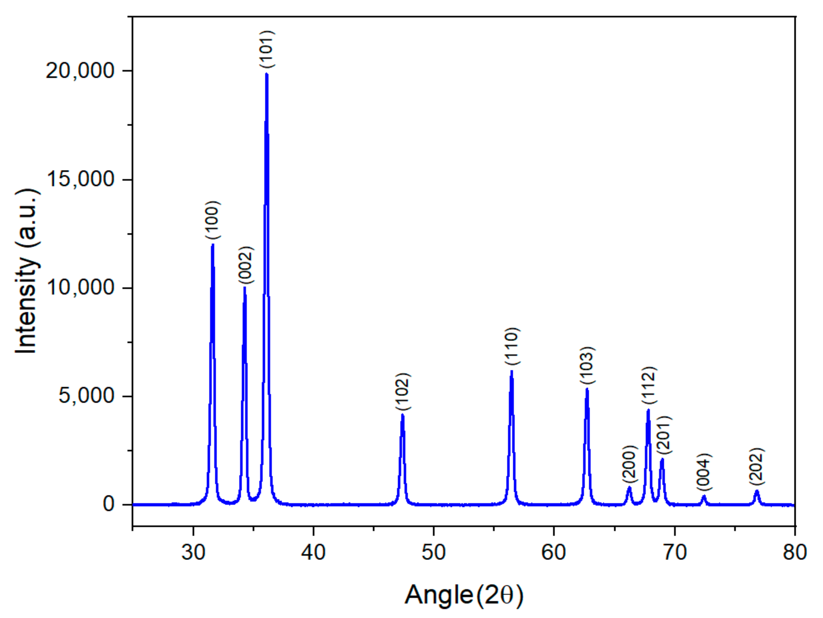
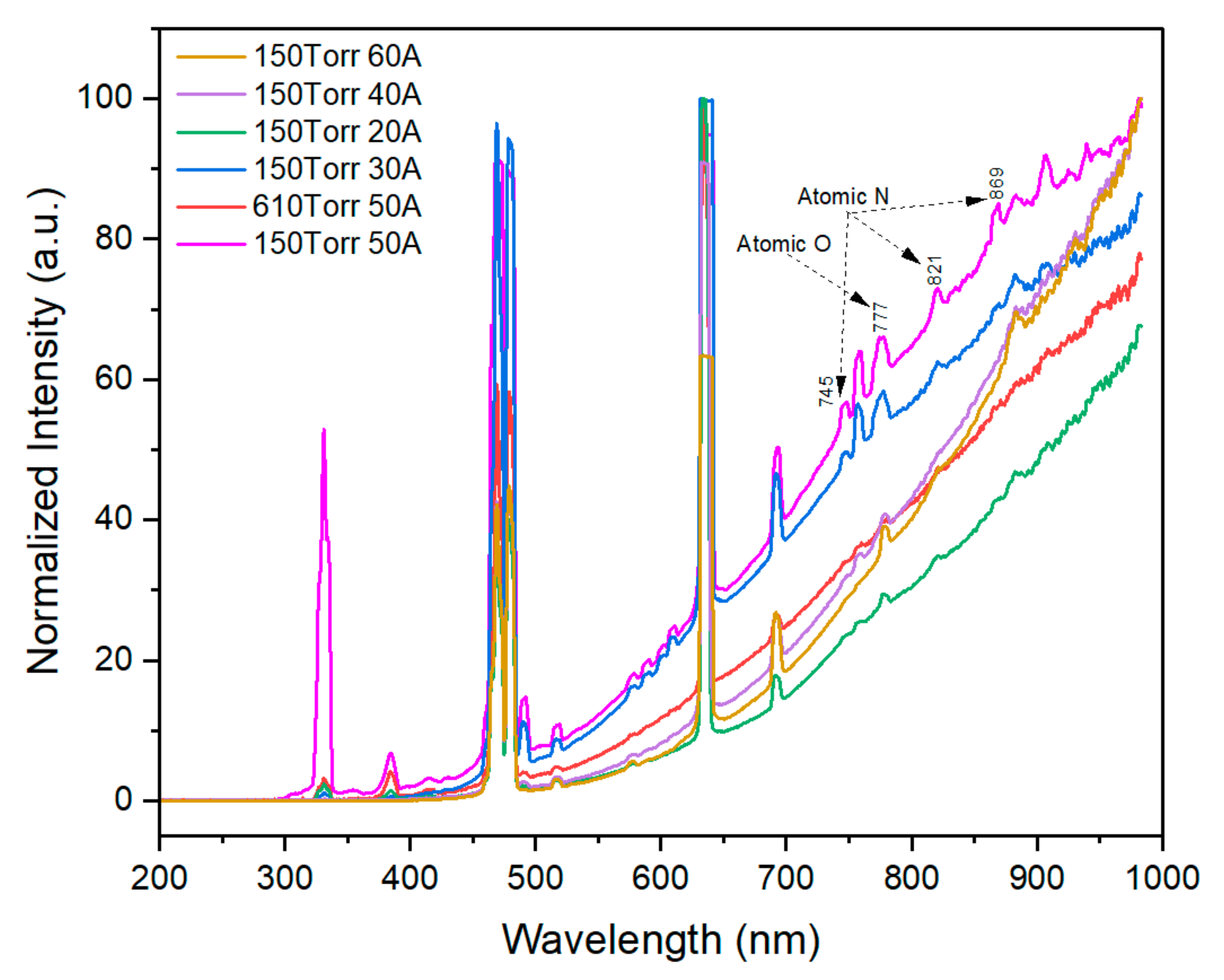
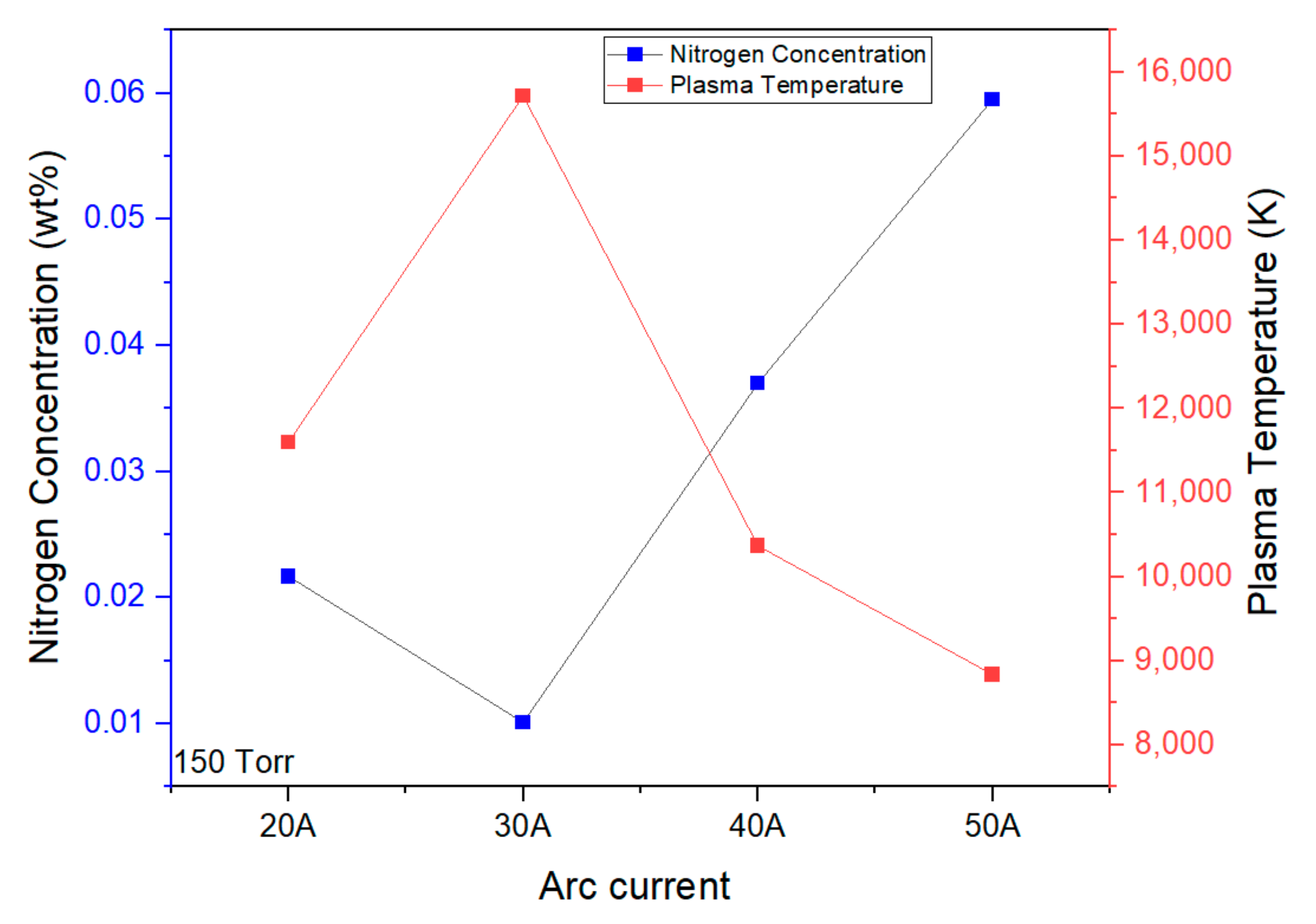
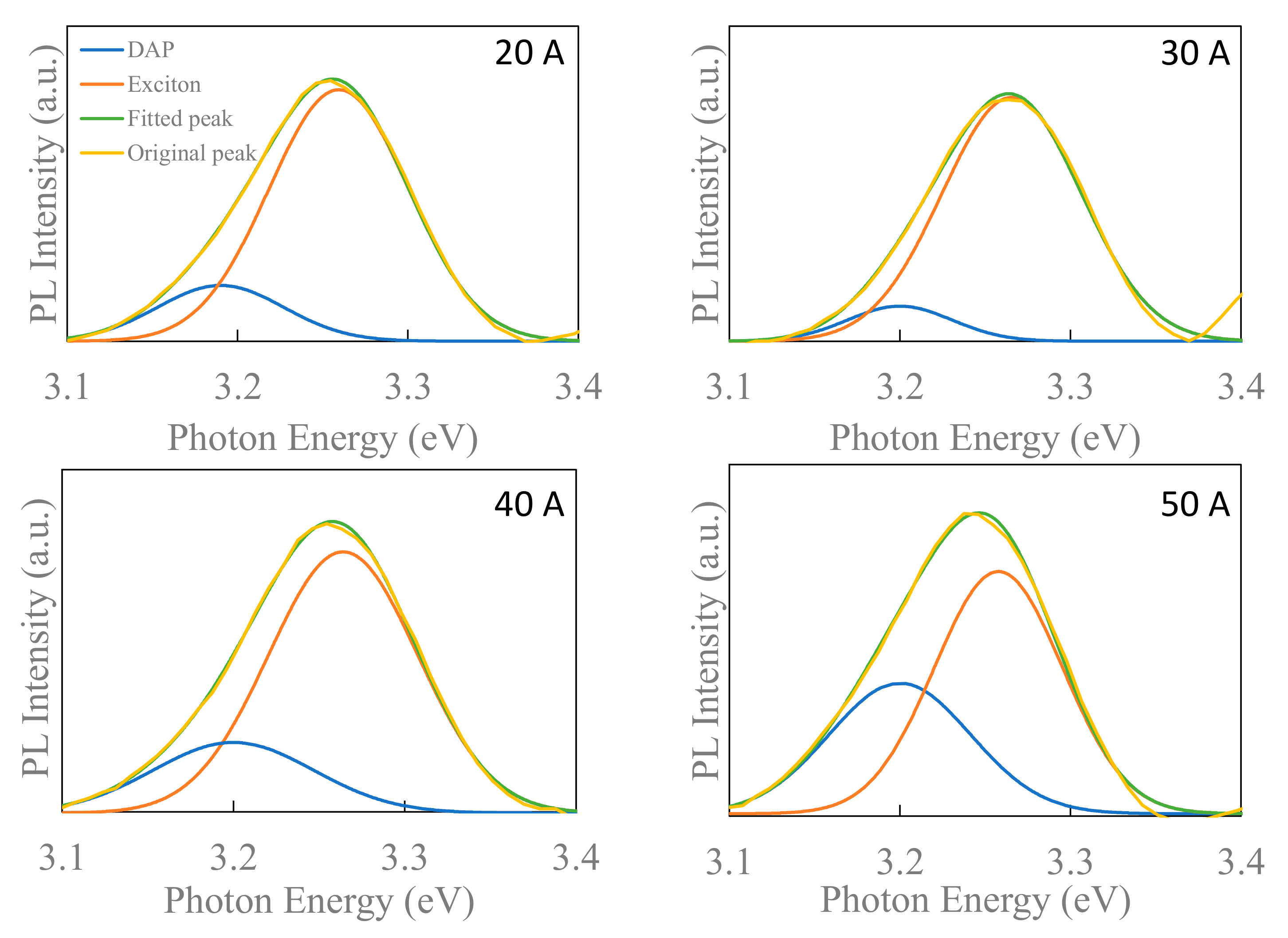
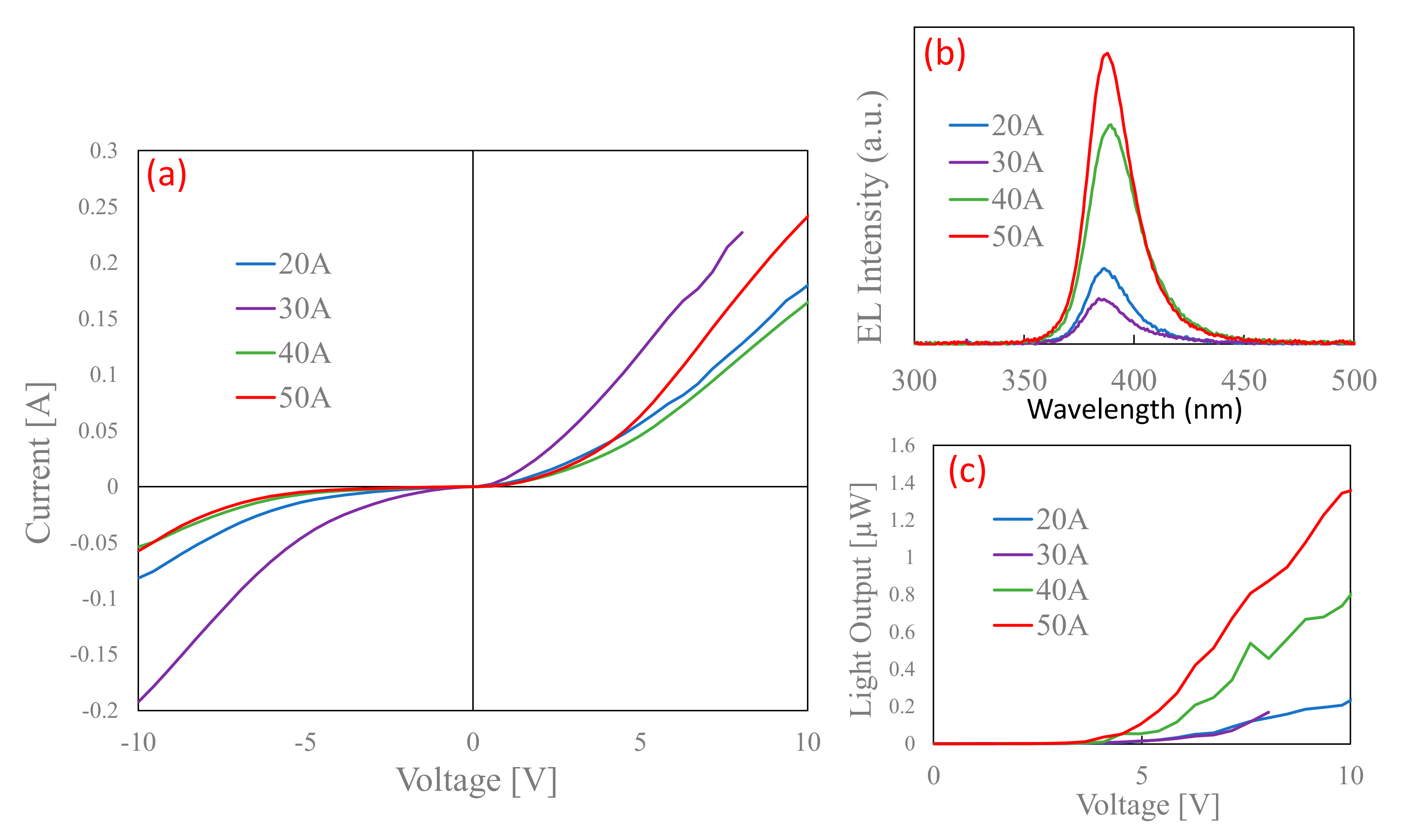
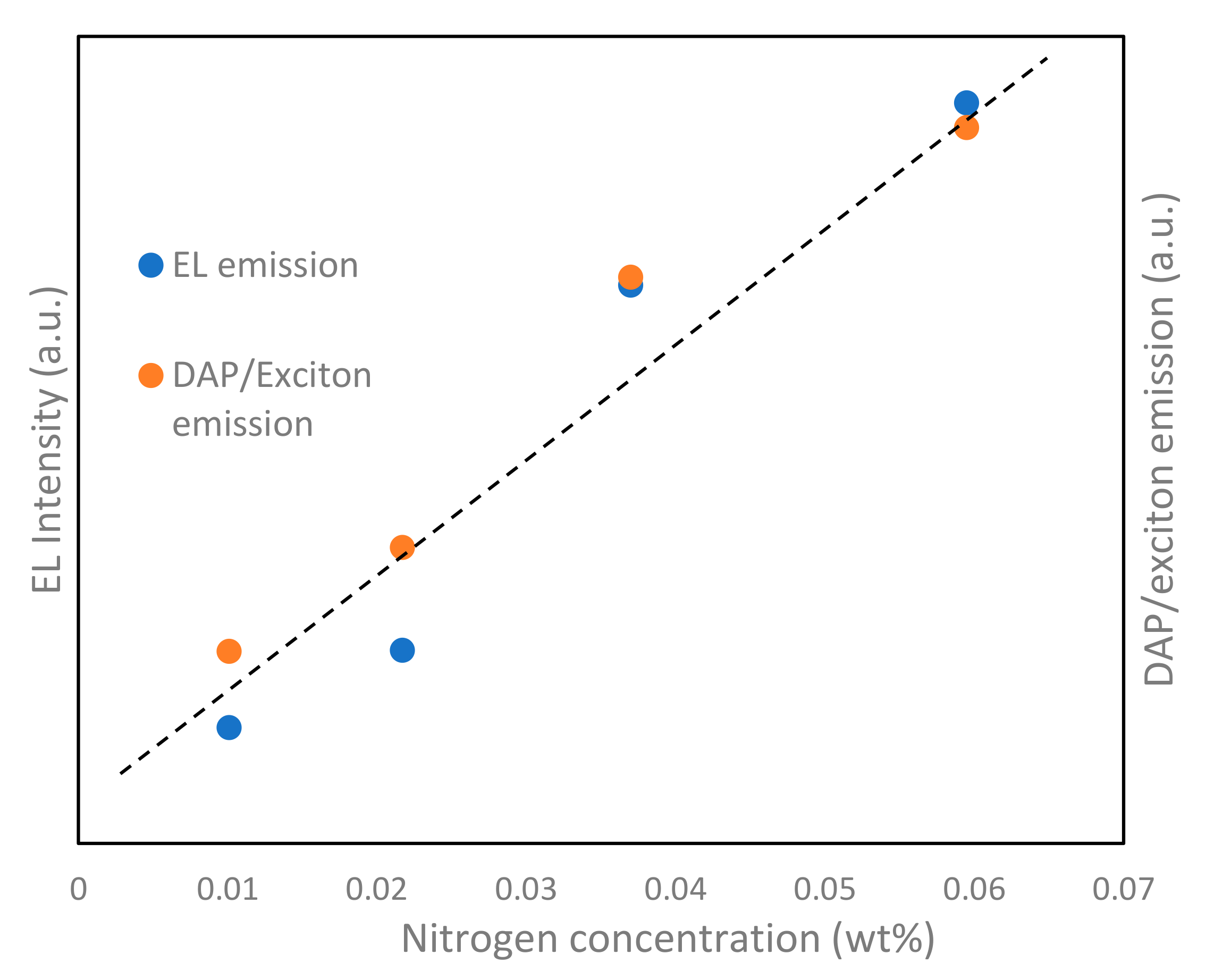
3. Results and Discussion

Zinc oxide NPs were deposited on the surface of the inner wall of the chamber, as shown in Figure 3, (a) before and (b) after the arc discharge. G.P. Zhu et al. discuss the mechanism for the formation of ZnO nanorods in the arc discharge, vapor–solid (VS), and vapor–liquid–solid (VLS) processes [30]. Our system follows a similar vapor–solid method, in which Zn metals were vaporized to zinc plasma due to the high temperatures during the arc discharge, and were later oxidized into ZnO nuclei, which were then condensed in the cooler end of the chamber (periphery) and formed nanorods/particles by absorbing gaseous plasma. Faster quenching in the arc discharge process leads to smaller-sized nanoparticles. The average hydrodynamic diameter of the ZnO NPs from the DLS results was around 200 nm. The size determined by the DLS method is always greater than the size determined by SEM due to the particle aggregation in the dispersion medium [35], as shown in Figure 3c. Different morphologies, such as tripods, and tetrapods, were observed in the SEM image, in addition to nanorods and nanoparticles.
The generated ZnO NPs were structurally characterized by XRD. Figure 4 shows the XRD pattern of the synthesized p-type ZnO NPs. No impurity peaks are observed, which indicates the high crystallization quality of the ZnO nanoparticles synthesized by the DC arc discharge method. The average crystallite size of the samples was estimated with the help of the Scherrer equation using diffraction intensities of (100), (002), and (101) planes. X-ray diffraction studies confirm that the synthesized materials are ZnO with the wurtzite phase, with the (101) plane as the favored plane. All the diffraction peaks agree with the reported Joint Committee on Powder Diffraction Standards (JCPDS), card number 36-1451 [34]. The average crystallite size of the NPs (tDs) that correspond to the most intense diffraction peaks at 2θ = 36.09°, as calculated by Debye–Scherrer’s equation and shown in Equation (1), is found to be 55.6 nm.
t D s = 0.9 λ β cos θ
where λ is the wavelength of the radiation, and β is the full width at half maximum (FWHM) of the diffraction peaks. The lattice constants are estimated by the hexagonal lattice parameters, where dhkl is the interplanar spacing of the (hkl) planes, determined from Bragg’s law: 2dhklsinθ = nλ. The lattice constants are calculated by the lattice parameters of the hexagonal close-packing (hcp) orientation for ZnO using the relation, as shown in Equation (2), in which a and c are found to be 3.258 Å and 5.221 Å, respectively. Further inspection of the XRD spectra shows that the position of the ZnO (002) peak shifts are likely due to the effects of the dopants, which prevent the complete relaxation of the stress [36].
1 d 2 = 4 3 h 2 + h k + k 2 a 2 + l 2 c 2
The unit cell volume (Vc = 3 / 2  a2 c) is 47.99 (Å)3, and the atomic packing factor (APF) (APF = 2πa/(3 3  c)) is calculated to be 0.754. The APF of bulk hexagonal ZnO materials is about 74% but in our case, the APF of ZnO NPs is close to 75% in a hexagonal structure. Other parameters are shown in Table 1.
The plasma properties were recorded by the OES setup, and the OES spectra were recorded during synthesis between 200 and 1000 nm (Figure 5). Both neutral as well as singly ionized zinc lines are present in this region, along with nitrogen and oxygen radicals. The zinc spectral line at 328.2 nm corresponds to the 4s4d 3D1 →4s4p 3P1 transition, the line at 468.0 nm corresponds to the 4s5s 3S1 → 4s4p 3P0 transition, and the line at 472.2 nm corresponds to the 4s5s 3S1 → 4s4p 3P1 transition. The strong resonance zinc line observed at 481.1 nm corresponds to the 4s5s 3S1 → 4s4p 3P2 transition. The assignment of these spectral lines was performed by referring to the NBS (NIST) database [37].
The high energy associated with the discharge dissociates gases in the form of plasma. The dissociation reaction of the mixture of gas plasma is explained by the following steps [38]:
O2 + e → 2O* + e,
N2 + O* → NO + N*,
NO + e → N* + O* + e,
The electron temperature was evaluated using the ratio of the relative intensity ratio of Zn(I) (481.05 and 636.2 nm in the OES) by the following relation, as shown in Equation (6):
I 1 I 2 = g 1 A 1 λ 2   e E 1 / k T e g 2 A 2 λ 1   e E 2 / k T e  
In this equation, subscripts 1 and 2 refer to the two spectral lines of the same element. The spectroscopic constants Ii, λi, gi, Ai, and Ei (i = 1, 2) represent the line intensity, wavelength, statistical weight, transition probability, and energy of the excited state, respectively. Te and k are the electron temperature and Boltzmann constant, respectively. These relevant spectroscopic constants are tabulated in Table 2 for the two emission lines of Zn(I), 4s5s 3S1→4s4p 3P2 at 481.05 nm and 4s 4d 1D2 → 4s4p 1P1 at 636.2 nm, and they were used to determine the electron temperature under the condition of local thermodynamic equilibrium (LTE). The atomic oxygen (O(I)) transition is at 777.1 nm, while N atom emissions at 745, 821, and 869 nm are observed from the OES [38]. Other possible optical transitions identified while fabricating ZnO NPs from DC arc plasma are referred to in previous reports [32].
We investigated the relationship between the plasma temperature and nitrogen content of the NPs, as shown in Figure 6. The plasma temperature is high during the initial phase of discharge and later saturates to a low value. Thermal energy is quickly changed into kinetic energy when plasma expands, which causes the temperature to drop. This rapid conversion of thermal energy into kinetic energy may account for the fall in its value [39].
Different conditions of nitrogen-doped ZnO NPs were fabricated at arc currents between 20 A and 50 A. The chamber pressure was maintained at 150 Torr/610 Torr with a constant gas flow rate of 5 L/min. In comparison with other fabrication methods, the ZnO NPs fabricated at 150 Torr and 50 A shows the lowest plasma temperature among all the conditions, as shown in Figure 6. The rapid expansion of plasma at a higher current density is thermalized due to the energy transfer to its surroundings. The intensity of the atomic N at the 869 nm line increases from 150 Torr (from 20 A to 50 A), as shown in Figure 5, to a maximum at 150 Torr and 50 A, which agrees with the nitrogen concentration measured from the inert gas method. High nitrogen content was observed in the previous report with 150 Torr and 30 A when the dry air was injected rather than pure mixture of oxygen and nitrogen gas [33]. High-chamber-pressure conditions (610 Torr) and a high current density (60 A) lead to a lower nitrogen content in ZnO NPs, and, therefore, to a reduction in the acceptor properties in the corresponding ZnO, which leads to lower electroluminescence emissions (not shown here).
Donor–acceptor pair (DAP) luminescence is a direct way to investigate the role of acceptors in ZnO. The presence of DAP recombination in the deconvolution of the photoluminescence (PL) spectra at the near-band-edge (NBE) emissions of the ZnO NP crystals suggests the presence of nitrogen acceptors [40]. The exciton (3.26eV concerning phonon replica) and DAP emissions of the deconvoluted NBE emissions are shown in Figure 7 [41]. The increase in the DAP intensity with the increase in the nitrogen concentration also shows the incorporation of nitrogen, which reinforces the claim that nitrogen acts as an acceptor, as described by Shafiqul et al. [33]. Here, the maximum DAP intensity is observed with the ZnO NPs fabricated at a chamber pressure of 150 Torr and a current of 50 A, which also have the maximum incorporated nitrogen. Note that the nitrogen concentration in ZnO NPs, measured by the thermal conductivity method, contains surface-absorbed species of nitrogen molecules.
For further verification, we fabricated LEDs using nitrogen-doped p-type ZnO NPs. Figure 8a shows the I–V results of the fabricated LEDs. The I–V characteristics reveal a diode-like rectification character with a low threshold voltage of 4.0 V at room temperature. Au contact with the p-type ZnO and n-type ZnO layer shows good ohmic behavior, as shown in previous works [42]. There is significant leakage current under all the fabricated conditions, which is mainly due to the binder parameters; however, it significantly improves during the fabrication with ZnO NPs obtained under higher current conditions. Figure 8b shows the corresponding EL spectra of the LEDs at a forward bias voltage of 8 V. The EL spectra show only near-band-edge UV emissions. The deep-level emissions are saturated by the higher current injection and are, thus, not observed in the EL spectra. Narrow EL spectra with a line width of 23 nm are observed peaking at 383 nm, which indicates the radiative annihilation of excitons [43]. The mechanism for the EL in the ZnO p–n junction should be discussed. Generally, the mobility of electrons is much larger than that of the holes in ZnO, and most of the electrons from the n-ZnO layer are injected into the p-ZnO layer, while only a few holes of the p-ZnO layer can enter into the n-ZnO layer [44]; however, in our case, the mobility of the holes is larger than that of the electrons because of the influence of the boundary layer [42], which may result in the movement of holes towards the n-layer, but does not contribute to the luminescence due to the high carrier concentration of n-layer. Thus, the emissions are dominant in the p-region. Figure 8c depicts the output power of the LEDs. The power of the LEDs was observed using Si-based photodiodes, which were placed on the bottom sides of the LEDs. LEDs fabricated with a chamber pressure of 150 Torr and under 50 A conditions have the maximum output power when compared with the other fabrication conditions, which validates the effect of nitrogen as an acceptor. Si-based photodiodes cannot receive all of the light from the device, and only a portion of the power is detected, which results in this comparatively low output power. The total EL power is roughly estimated to be about 12 times larger than the measured value [34]. To further study the relationship with the variable nitrogen concentration, the ratio of the DAP/exciton emissions observed from the PL results was compared with the EL results of the LED, as shown in Figure 9. In the figure, a linear relationship can be observed for both the EL intensity and DAP/exciton emissions. Shafiqul et al. also reported a similar relationship, even under different plasma conditions, which buttresses the role of nitrogen as an acceptor [33]. Thus, the DAP luminescence is directly affected by the presence of nitrogen in ZnO NPs and the device’s performance.

4. Conclusions

DC arc plasma gas evaporation was used to successfully fabricate nitrogen-doped ZnO nanoparticles and spectroscopically evaluate the generation process. The incorporation of the nitrogen dopants is favorable at the low plasma temperature, and they act as acceptors in the ZnO NPs, which is further validated by the fabrication of nanoparticle-based LEDs. The constructed homojunction LEDs exhibit diode-like characteristics, emitting UV emission peaking at 383 nm with a line width of about 23 nm. Overall, the experimental results indicate that nitrogen dopant most likely operates as an acceptor for ZnO NPs, and this is optimised spectroscopically.

Author Contributions

R.D. performed all experiments including material synthesis and characterization, T.A. performed some of the device fabrication and characterization, T.Y. and Y.F. were involved in planning and supervising the study. T.Y. contributed to setting up the spin coating and assisted in XRD and I-V evaluations. R.D. wrote the manuscript in consultation with T.Y. and Y.F. All authors have read and agreed to the published version of the manuscript.

Funding

This work was partially supported by MEXT of Japan City Area Program of Shinji Lake and Nakaumi (2009–2012), JSPS KAKENHI Grant Number 25630150, The Canon Foundation, and S-Nanotech Co-Creation Co., Ltd.

Institutional Review Board Statement

Not applicable.

Informed Consent Statement

Not applicable.

Data Availability Statement

The data that support the finding of this study are available on request from the corresponding author. The data are not publicly available due to privacy or ethical restrictions.

Acknowledgments

The authors are grateful to the cooperation of the Centre for Integrated Research in Science, Shimane University, for providing XRD and FE-SEM analysis.

Conflicts of Interest

The author Raj Deep, Takuma Akazawa and Toshiyuki Yoshida declare that they have no known competing financial interests or personal relationship that could have appeared to influence the work reported in this paper. Yasuhisa Fujita (Professor of Shimane University) is CEO of S-Nanotech Co-Creation Co., Ltd. (SNCC). This study was partially supported by a joint research fund of SNCC.

References

  1. Tsukazaki, A.; Ohtomo, A.; Onuma, T.; Ohtani, M.; Makino, T.; Sumiya, M.; Ohtani, K.; Chichibu, S.F.; Fuke, S.; Segawa, Y.; et al. Repeated temperature modulation epitaxy for p-type doping and light-emitting diode based on ZnO. Nat. Mater. 2005, 4, 42–46. [Google Scholar] [CrossRef]
  2. Chu, S.; Wang, G.; Zhou, W.; Lin, Y.; Chernyak, L.; Zhao, J.; Kong, J.; Li, L.; Ren, J.; Liu, J. Electrically pumped waveguide lasing from ZnO nanowires. Nat. Nanotechnol. 2011, 6, 506–510. [Google Scholar] [CrossRef] [PubMed]
  3. Deka Boruah, B. Zinc oxide ultraviolet photodetectors: Rapid progress from conventional to self-powered photodetectors. Nanoscale Adv. 2019, 1, 2059–2085. [Google Scholar] [CrossRef] [PubMed] [Green Version]
  4. Qi, K.; Cheng, B.; Yu, J.; Ho, W. Review on the improvement of the photocatalytic and antibacterial activities of ZnO. J. Alloy. Compd. 2017, 727, 792–820. [Google Scholar] [CrossRef]
  5. Cao, C.; Zhang, B.; Lin, S. p-type ZnO for photocatalytic water splitting. APL Mater. 2022, 10, 030901. [Google Scholar] [CrossRef]
  6. Miller, D.R.; Akbar, S.A.; Morris, P.A. Nanoscale metal oxide-based heterojunctions for gas sensing: A review. Sens. Actuators B Chem. 2014, 204, 250–272. [Google Scholar] [CrossRef]
  7. Wang, Z.L.; Yang, R.; Zhou, J.; Qin, Y.; Xu, C.; Hu, Y.; Xu, S. Lateral nanowire/nanobelt based nanogenerators, piezotronics and piezo-phototronics. Mater. Sci. Eng. R Rep. 2010, 70, 320–329. [Google Scholar] [CrossRef]
  8. Senthilkumar, K.; Senthilkumar, O.; Yamauchi, K.; Sato, M.; Morito, S.; Ohba, T.; Nakamura, M.; Fujita, Y. Preparation of ZnO nanoparticles for bio-imaging applications. Phys. Status Solidi B 2009, 246, 885–888. [Google Scholar] [CrossRef]
  9. Saadi, H.; Benzarti, Z.; Sanguino, P.; Pina, J.; Abdelmoula, N.; de Melo, J.S.S. Enhancing the electrical conductivity and the dielectric features of ZnO nanoparticles through Co doping effect for energy storage applications. J. Mater. Sci. Mater. Electron. 2023, 34, 116. [Google Scholar] [CrossRef]
  10. Saadi, H.; Benzarti, Z.; Rhouma, F.I.H.; Sanguino, P.; Guermazi, S.; Khirouni, K.; Vieira, M.T. Enhancing the electrical and dielectric properties of ZnO nanoparticles through Fe doping for electric storage applications. J. Mater. Sci. Mater. Electron. 2021, 32, 1536–1556. [Google Scholar] [CrossRef]
  11. Rahman, F. Zinc oxide light-emitting diodes: A review. Opt. Eng. 2019, 58, 1. [Google Scholar] [CrossRef] [Green Version]
  12. Chen, M.-J.; Yang, J.-R.; Shiojiri, M. ZnO-based ultra-violet light emitting diodes and nanostructures fabricated by atomic layer deposition. Semicond. Sci. Technol. 2012, 27, 074005. [Google Scholar] [CrossRef]
  13. Yuen, C.; Yu, S.F.; Lau, S.P.; Rusli; Chen, T.P. Fabrication of n-ZnO:Al∕p-SiC(4H) heterojunction light-emitting diodes by filtered cathodic vacuum arc technique. Appl. Phys. Lett. 2005, 86, 241111. [Google Scholar] [CrossRef]
  14. Baltakesmez, A.; Tekmen, S.; Köç, P.; Tüzemen, S.; Meral, K.; Onganer, Y. UV-visible detector and LED based n-ZnO/p-Si heterojunction formed by electrodeposition. AIP Adv. 2013, 3, 032125. [Google Scholar] [CrossRef]
  15. Shan, C.X.; Liu, J.S.; Lu, Y.J.; Li, B.H.; Ling, F.C.C.; Shen, D.Z. p-type doping of MgZnO films and their applications in optoelectronic devices. Opt. Lett. 2015, 40, 3041. [Google Scholar] [CrossRef] [PubMed]
  16. Zhang, T.; Li, M.; Chen, J.; Wang, Y.; Miao, L.; Lu, Y.; He, Y. Multi-component ZnO alloys: Bandgap engineering, hetero-structures, and optoelectronic devices. Mater. Sci. Eng. R Rep. 2022, 147, 100661. [Google Scholar] [CrossRef]
  17. Look, D.C.; Claflin, B. P-type doping and devices based on ZnO. Phys. Status Solidi B 2004, 241, 624–630. [Google Scholar] [CrossRef]
  18. Park, C.H.; Zhang, S.B.; Wei, S.-H. Origin of p -type doping difficulty in ZnO: The impurity perspective. Phys. Rev. B 2002, 66, 073202. [Google Scholar] [CrossRef]
  19. Fujita, Y.; Moriyama, K.; Hiragino, Y.; Furubayashi, Y.; Hashimoto, H.; Yoshida, T. Electroluminescence from nitrogen doped ZnO nanoparticles. Phys. Status Solidi C 2014, 11, 1260–1262. [Google Scholar] [CrossRef]
  20. Fujita, Y.; Yanase, S.; Nishikori, H.; Hiragino, Y.; Furubayashi, Y.; Lin, J.; Yoshida, T. Near ultraviolet light emitting diodes using ZnMgO:N/ZnO hetero-junction grown by MOVPE. J. Cryst. Growth 2017, 464, 226–230. [Google Scholar] [CrossRef]
  21. Dai, X.; Zhang, Z.; Jin, Y.; Niu, Y.; Cao, H.; Liang, X.; Chen, L.; Wang, J.; Peng, X. Solution-processed, high-performance light-emitting diodes based on quantum dots. Nature 2014, 515, 96–99. [Google Scholar] [CrossRef] [PubMed]
  22. Lei, J.F.; Wang, Z.W.; Li, W.S. Controlled fabrication of ordered structure-based ZnO films by electrochemical deposition. Thin Solid Films 2014, 573, 74–78. [Google Scholar] [CrossRef]
  23. Sun, H.; Zhang, Q.; Zhang, J.; Deng, T.; Wu, J. Electroluminescence from ZnO nanowires with a p-ZnO film/n-ZnO nanowire homojunction. Appl. Phys. B 2008, 90, 543–546. [Google Scholar] [CrossRef]
  24. Sang, N.X.; Beng, T.C.; Jie, T.; Fitzgerald, E.A.; Jin, C.S. Fabrication of p-type ZnO nanorods/n-GaN film heterojunction ultraviolet light-emitting diodes by aqueous solution method. Phys. Status Solidi A 2013, 210, 1618–1623. [Google Scholar] [CrossRef]
  25. Hasnidawani, J.N.; Azlina, H.N.; Norita, H.; Bonnia, N.N.; Ratim, S.; Ali, E.S. Synthesis of ZnO Nanostructures Using Sol-Gel Method. Procedia Chem. 2016, 19, 211–216. [Google Scholar] [CrossRef] [Green Version]
  26. Aneesh, P.M.; Vanaja, K.A.; Jayaraj, M.K. Synthesis of ZnO Nanoparticles by Hydrothermal Method; Gaburro, Z., Cabrini, S., Eds.; SPIE: San Diego, CA, USA, 2007; p. 66390J. [Google Scholar]
  27. Wojnarowicz, J.; Chudoba, T.; Lojkowski, W. A Review of Microwave Synthesis of Zinc Oxide Nanomaterials: Reactants, Process Parameters and Morphologies. Nanomaterials 2020, 10, 1086. [Google Scholar] [CrossRef]
  28. Avdeeva, A.V.; Zang, X.; Muradova, A.G.; Yurtov, E.V. Formation of Zinc-Oxide Nanorods by the Precipitation Method. Semiconductors 2017, 51, 1724–1727. [Google Scholar] [CrossRef]
  29. Hiragino, Y.; Tanaka, T.; Takeuchi, H.; Takeuchi, A.; Lin, J.; Yoshida, T.; Fujita, Y. Synthesis of nitrogen-doped ZnO nanoparticles by RF thermal plasma. Solid-State Electron. 2016, 118, 41–45. [Google Scholar] [CrossRef]
  30. Zhu, G.P.; Xu, C.X.; Wu, X.F.; Yang, Y.; Sun, X.W.; Cui, Y.P. Zinc Oxide Nanorods Grown by Arc Discharge. J. Electron. Mater. 2007, 36, 494–497. [Google Scholar] [CrossRef]
  31. Ko, T.S.; Yang, S.; Hsu, H.C.; Chu, C.P.; Lin, H.F.; Liao, S.C.; Lu, T.C.; Kuo, H.C.; Hsieh, W.F.; Wang, S.C. ZnO nanopowders fabricated by dc thermal plasma synthesis. Mater. Sci. Eng. B 2006, 134, 54–58. [Google Scholar] [CrossRef]
  32. Senthilkumar, K.; Senthilkumar, O.; Morito, S.; Ohba, T.; Fujita, Y. Synthesis of zinc oxide nanoparticles by dc arc dusty plasma. J. Nanoparticle Res. 2012, 14, 1205. [Google Scholar] [CrossRef]
  33. Shafiqul, I.M.; Deep, R.; Lin, J.; Yoshida, T.; Fujita, Y. The Role of Nitrogen Dopants in ZnO Nanoparticle-Based Light Emitting Diodes. Nanomaterials 2022, 12, 358. [Google Scholar] [CrossRef] [PubMed]
  34. Shafiqul, I.M.; Deep, R.; Lin, J.; Yoshida, T.; Fujita, Y. Demonstration and Evaluation of p-Type and n-Type ZnO Nanoparticles-Based Homojunction UV Light-Emitting Diodes. Phys. Status Solidi RRL—Rapid Res. Lett. 2022, 16, 2100556. [Google Scholar] [CrossRef]
  35. Domingos, R.F.; Baalousha, M.A.; Ju-Nam, Y.; Reid, M.M.; Tufenkji, N.; Lead, J.R.; Leppard, G.G.; Wilkinson, K.J. Characterizing Manufactured Nanoparticles in the Environment: Multimethod Determination of Particle Sizes. Environ. Sci. Technol. 2009, 43, 7277–7284. [Google Scholar] [CrossRef]
  36. Li, D.; Wang, H.-Q.; Zhou, H.; Li, Y.-P.; Huang, Z.; Zheng, J.-C.; Wang, J.-O.; Qian, H.; Ibrahim, K.; Chen, X.; et al. Influence of nitrogen and magnesium doping on the properties of ZnO films. Chin. Phys. B 2016, 25, 076105. [Google Scholar] [CrossRef]
  37. Hanif, M.; Salik, M.; Baig, M.A. Laser Based Optical Emission Studies of Zinc Oxide (ZnO) Plasma. Plasma Chem. Plasma Process. 2013, 33, 1167–1178. [Google Scholar] [CrossRef]
  38. Kato, H.; Yamamuro, T.; Ogawa, A.; Sano, M. Impact of Mixture Gas Plasma of N2 and O2 as the N Source on ZnO-Based Ultraviolet Light-Emitting Diodes Fabricated by Molecular Beam Epitaxy. Appl. Phys. Express 2011, 4, 091105. [Google Scholar] [CrossRef]
  39. Shaikh, N.M.; Rashid, B.; Hafeez, S.; Jamil, Y.; Baig, M.A. Measurement of electron density and temperature of a laser-induced zinc plasma. J. Phys. Appl. Phys. 2006, 39, 1384–1391. [Google Scholar] [CrossRef]
  40. Xiong, G.; Ucer, K.B.; Williams, R.T.; Lee, J.; Bhattacharyya, D.; Metson, J.; Evans, P. Donor-acceptor pair luminescence of nitrogen-implanted ZnO single crystal. J. Appl. Phys. 2005, 97, 043528. [Google Scholar] [CrossRef]
  41. Yang, S.; Tian, X.; Wang, L.; Wei, J.; Qi, K.; Li, X.; Xu, Z.; Wang, W.; Zhao, J.; Bai, X.; et al. In-situ optical transmission electron microscope study of exciton phonon replicas in ZnO nanowires by cathodoluminescence. Appl. Phys. Lett. 2014, 105, 071901. [Google Scholar] [CrossRef]
  42. Itohara, D.; Shinohara, K.; Yoshida, T.; Fujita, Y. p-Channel and n-Channel Thin-Film-Transistor Operation on Sprayed ZnO Nanoparticle Layers. J. Nanomater. 2016, 2016, 1–6. [Google Scholar] [CrossRef] [Green Version]
  43. Guo, L.; Ji, Y.L.; Xu, H.; Simon, P.; Wu, Z. Regularly Shaped, Single-Crystalline ZnO Nanorods with Wurtzite Structure. J. Am. Chem. Soc. 2002, 124, 14864–14865. [Google Scholar] [CrossRef] [PubMed]
  44. Chen, A.; Zhu, H.; Wu, Y.; Chen, M.; Zhu, Y.; Gui, X.; Tang, Z. Beryllium-Assisted p-Type Doping for ZnO Homojunction Light-Emitting Devices. Adv. Funct. Mater. 2016, 26, 3696–3702. [Google Scholar] [CrossRef]
Figure 1. Schematic diagram of arc discharge apparatus.
J 06 00016 g001
Figure 2. Schematic diagram of ZnO NP-based LED.
J 06 00016 g002
Figure 3. Chamber (a) before and (b) after arc discharge. (c) SEM of ZnO NPs (inset shows DLS spectra).
J 06 00016 g003
Figure 4. XRD pattern of p-type ZnO NPs.
J 06 00016 g004
Figure 5. OES spectra during synthesis.
J 06 00016 g005
Figure 6. Plasma temperature and N concentration.
J 06 00016 g006
Figure 7. Deconvoluted PL emissions of near-band-edge emission regions.
J 06 00016 g007
Figure 8. (a) I-V characteristics, (b) EL spectra, and (c) output power of p-ZnO/GZO LEDs fabricated using ZnO NPs prepared at chamber pressure of 150 Torr and with arc currents ranging from 20 to 50 A.
J 06 00016 g008
Figure 9. Ratio of DAP/exciton emissions and EL intensities with variable nitrogen concentration.
J 06 00016 g009
Table 1. XRD parameters of p-type ZnO NPs.
Parameters(100)(002)(101)
2θ (degree)31.6134.2636.09
FWHM (degree)0.1570.1390.156
dhkl (Å)2.8272.6142.486
Crystallite size (nm)54.962.455.6
a (Å)3.258
c (Å)5.221
c/a1.60
Unit cell vol (Å)347.99
APF0.754
Table 2. Spectroscopic parameters of the neutral zinc (Zn I) lines.
Wavelength
λ (nm)
TransitionsStatistical
Weight g
Transition
Probability A (s−1)
Excitation Energy
E (cm−1)
481.054s5s 3S1 → 4s4p 3P237.00 × 10753,672.24
636.234s4d 1D2 → 4s4p 1P154.65 × 10762,458.51
Disclaimer/Publisher’s Note: The statements, opinions and data contained in all publications are solely those of the individual author(s) and contributor(s) and not of MDPI and/or the editor(s). MDPI and/or the editor(s) disclaim responsibility for any injury to people or property resulting from any ideas, methods, instructions or products referred to in the content.

