Article

Characterization of Bipolar Transport in Hf(Te1−xSex)2 Thermoelectric Alloys

Department of Materials Science and Engineering, University of Seoul, 163 Seoulsiripdae-ro, Dongdaemun-gu, Seoul 02504, Republic of Korea
*
Author to whom correspondence should be addressed.
These authors contributed equally to this work.
Ceramics 2023, 6(1), 538-547; https://doi.org/10.3390/ceramics6010032
Submission received: 27 December 2022 / Revised: 1 February 2023 / Accepted: 14 February 2023 / Published: 17 February 2023
(This article belongs to the Special Issue Thermoelectric Properties of Ceramic-Based Materials)

Abstract

:
Control of bipolar conduction is essential to improve the high-temperature thermoelectric performance of materials for power generation applications. Recently, Hf(Te1−xSex)2 alloys have gained much attention due to their potential use in thermoelectric power generation. Increasing the Se alloying content significantly increases the band gap while decreasing its carrier concentration. These two factors affect bipolar conduction substantially. In addition, the weighted mobility ratio is estimated from the experimental electronic transport properties of Hf(Te1−xSex)2 alloys (x = 0.0, 0.025, 0.25, 0.5, 1.0) by using the Two-Band model. From the bipolar thermal conductivity also calculated using the Two-Band model, we find that it peaks near x = 0.5. The initial bipolar conductivity increase of x < 0.5 is mostly due to the decrease in the weighted mobility ratio and carrier concentration with increasing x. For x > 0.5, the drop in the bipolar conductivity can be understood with significant band gap enlargement.

1. Introduction

Thermoelectric technology can be used to harvest electricity from waste heat. Because the burning of no fossil fuels is required to produce electricity, the demand for thermoelectric technology is growing fast. The process of generating electricity using the thermoelectric device is also simple. When one side of the thermoelectric device (p- and n-type thermoelectric elements connected in series) is attached to the waste heat source, the induced temperature gradient across the device makes holes (in the p-type element) and electrons (in the n-type element) move away from the heat source while generating electricity [1,2,3,4,5]. The conversion (from heat to electricity) efficiency of the thermoelectric device is largely determined by the thermoelectric performance of the materials used in the device. Most importantly, how much electric voltage is induced within the thermoelectric material due to the applied temperature gradient is defined as the Seebeck coefficient (S). To achieve high conversion efficiency in the thermoelectric device, thermoelectric materials with high S is desired. However, the thermoelectric performance of a material is better represented by a Figure-of-merit zT than the S alone. The zT is defined as Equation (1) [6].
z T = S 2 σ T κ e + κ l
The σ, κe, κl, and T are the electrical conductivity, thermal conductivity by charged carriers, lattice thermal conductivity, and temperature (unit of K), respectively. According to Equation (1), the S and σ (electronic properties) need to be improved while suppressing κe and κl (thermal properties) to enhance zT. The thermoelectric parameters in Equation (1) are interconnected with one another, except κl. If the σ is increased by increasing the Hall carrier concentration (nH), the S will decrease but κe will increase. For this reason, the zT is always optimized at a narrow range of nH. To avoid any complication, many researchers have focused on reducing κl or the engineering band structure to overcome the strong Sσ trade-off relation [7,8,9,10,11,12,13]. The strong Sσ trade-off relation observed in thermoelectric materials is mainly due to the density-of-states effective mass (md*) of the material. At a fixed carrier concentration, increasing md* increases the S while decreasing the σ. However, more specifically, the S is related to the md*, but the σ is related to the single band mass (mb) and not to the md* directly. Of course, the md* is a product of mb and the number of valley degeneracy to the power of 2/3 (NV 2/3). If we can increase the S without decreasing σ, the strong Sσ trade-off relationship can be overcome. It can be achieved if the increase in S is due to NV increase and not the mb increase. The improvement of S via the NV increase can be achieved by converging adjacent bands, and in this case, σ will remain intact.
As one of the approaches to bypass the Sσ trade-off relationship, semiconducting transition metal dichalcogenides (TMDs) have been studied extensively because of their novel electronic and thermal properties [14,15,16,17,18,19,20]. According to Yumnam et al., HfX2 (X = S, Se) compounds exhibit high theoretical S and σ at the same time, stemming from the interaction between the light and heavy bands. In addition, they show significantly low theoretical κl (< 2 W m−1 K−1) due to the low phonon group velocity [21]. Recently, Bang et al. have reported experimental electronic transport properties of bulk Hf(Te1−xSex)2 alloys (x = 0.0–1.0). A high-power factor (PF = S2σ) of 0.24 mW m−1 K−1 is obtained for HfTe2 at 600 K [22]. They also provide how band parameters such as the md*, non-degenerate mobility (μ0), and weighted mobility (μW) change as the Se alloying content increases from 0.0 (HfTe2) to 1.0 (HfSe2) using the Single Parabolic Band (SPB) model [23]. Based on the SPB model, increasing the Se alloying content sharply decreases md*, μ0, and μW. Bang et al. also report that the band gap estimated by using the Goldsmid–Sharp equation increases significantly with the increasing Se alloying content [24,25]. However, the effect of the band gap increase was not taken into consideration when estimating the electronic band parameters.
Here, the effect of the band gap change in the electronic transport properties of bulk Hf(Te1−xSex)2 alloys (x = 0.0, 0.025, 0.25, 0.5, and 1.0) is investigated using the Two-Band (TB) model. Experimental nH-dependent S and Hall mobility (μH) are used to estimate md,i*, μ0,i, and μW,i (i = maj for majority carrier band and min for minority carrier band) for one valence band and one conduction band that contribute to electronic transport. From the individual band parameter for each band, the ratio of majority carrier-weighted mobility to minority carrier-weighted mobility, A, and bipolar thermal conductivity (κb) are also characterized. The calculated κb at 300 K peaks when x = 0.5, and this is an interplay among A, the Goldsmid–Sharp band gap (Eg,G-S), and nH that are known to affect the κb, but change differently with increasing x.

2. Materials and Methods

The ingots of Hf(Te1−xSex)2 (x = 0, 0.025, 0.25, 0.5, and 1) were first prepared using melting stoichiometrically weighed Hf (99.6%), Te (99.999%), and Se (99.999%) powders within vacuum quartz tubes at 950 °C for 60 h. The ingots were transferred to a glove box and pulverized in the glove box into powders using a mortar and pestle. The powders were then sintered using a spark plasma sintering at 580 °C for 10 min under 50 MPa in a vacuum. The Hall carrier concentration and Hall mobility of the sintered samples were obtained from the Hall coefficient measured via the Van der Pauw method using a commercial Hall measurement system (AHT-55T5 from Ecopia, Anyang, South Korea) under a magnetic field of 0.5 T. For the samples with low Hall mobility, a very thin sample (~ 500 μm) is fabricated to minimize measurement errors.
The md,i* and μ0,i (i = maj, min) are fitted to the experimental nH-dependent S and σ, respectively, using the TB model. According to the TB model, the Si, σi, and Hall coefficient (RH,i) (i = maj, min) are defined as below.
S m a j = k B e ( 2 F 1 ( η ) F 0 ( η ) η )
S m i n = k B e ( 2 F 1 ( η ε g ) F 0 ( η ε g ) + η + ε g )
S = S m a j σ m a j + S m i n σ m i n σ m a j + σ m i n
σ m a j = ( e 3 h 5 48 2 π 5 ) μ 0 , m a j ( m d , m a j * k B T ) 3 / 2 F 0 ( η )
σ m i n = ( e 3 h 5 48 2 π 5 ) μ 0 , m i n ( m d , m i n * k B T ) 3 / 2 F 0 ( η ε g )
σ = σ m a j + σ m i n
1 R H , m a j = 16 π e 3 ( 2 m d , m a j * k B T h 2 ) 3 / 2 ( F 0 ( η ) ) 2 F 1 / 2 ( η )
1 R H , m i n = 16 π e 3 ( 2 m d , m i n * k B T h 2 ) 3 / 2 ( F 0 ( η ε g ) ) 2 F 1 / 2 ( η ε g )
R H = R H , m a j σ m a j 2 + R H , m i n σ m i n 2 ( σ m a j + σ m i n ) 2
n H = 1 R H e
The kB, e, η, h, εg, and Fj are the Boltzmann constant, electric charge, fermi level, Planck constant, band gap divided by kBT, and Fermi integral of order j (Equation (12)).
F j ( η ) = 0 ε j 1 + exp ( ε η ) d ε
The calculated S (Equation (4)) as a function of nH (Equation (11)) is fitted to the measurement to obtain md,i* (i = maj, min). The calculated σ (Equation (7)) as a function of nH (Equation (11)) is fitted to the measurement to obtain μ0,i (i = maj, min). The εg for Hf(Te1−xSex)2 (x = 0.0, 0.025, 0.25, 0.5, and 1.0) are adopted from Bang et al. and they are listed in the Table 1 below [22]. In a Single Parabolic Band (SPB) model, where we assume there is only one band participating in the electronic transport properties, we only have to fit one band parameter, which is the md* to the experimental nH-dependent S. However, in the TB model, the total S is an electrical conductivity-weighted average between Smaj and Smin (Equation (4)). In other words, when there are two bands participating in transport, even when we want to describe the experimental nH-dependent S, both md,i* (i = maj, min) and μ0,i (i = maj, min) need to be fitted simultaneously while changing the εg for different x. Therefore, instead of fitting md* from the nH-dependent S and μ0 from the nH-dependent σ, consecutively, all four unknown band parameters md,i* (i = maj, min) and μ0,i (i = maj, min) were fitted to nH-dependent S and σ concurrently. Plus, to minimize the complexity of the TB modeling, once the md,imin* and μ0,min were fitted in x with the lowest εg (where the contribution from the minority carrier band is maximum), they were kept constant for the TB model calculation of the samples with different x. This is because the impact of the minority carrier band on the electronic transport properties decreases with an increasing εg.
The μW,i is characterized from the estimated md,i* and μ0,i (i = maj, min) via Equation (13) (m0 is the electron rest mass).
μ W , i = μ 0 , i ( m d , i * m 0 ) 3 / 2
The weighted mobility ratio a is computed using Equation (14).
A = μ W , m a j μ W , m i n

3. Results and Discussion

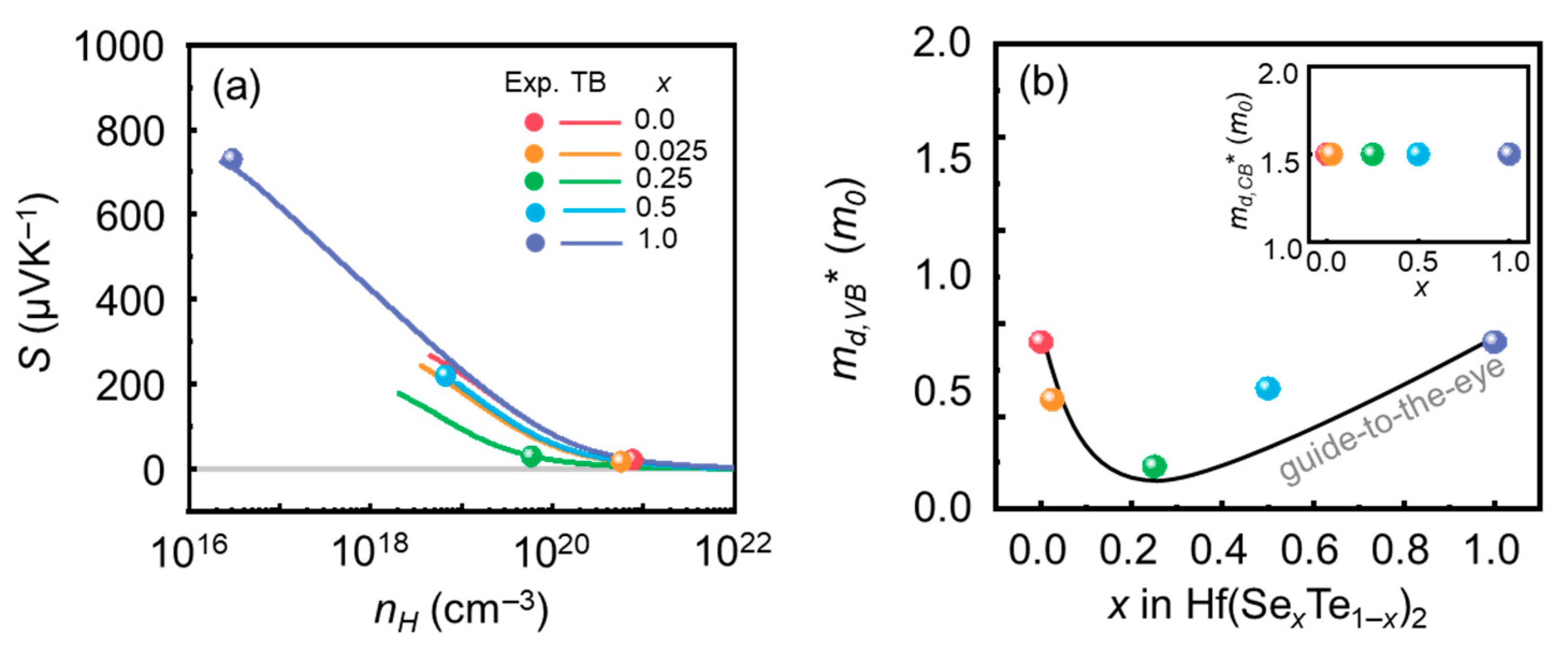
3.1. Estimation of the md,i* (i = VB, CB) Via the TB Model

Figure 1a presents the experimental S in terms of nH at 300 K adopted from Bang et al. (in symbols) [22]. The magnitude of S drastically increases with the increasing Se alloying content (x). While S of the samples with x ≤ 0.25 is smaller than 30 μV K1, the S of x = 0.5 and x = 1.0 amount to 220 and 730 μV K1, respectively. On the contrary, measured nH significantly decrease with increasing x. For example, the nH of x = 0.0, which is 7.7 × 1020 cm3, sharply decreases to 3.0 × 1016 cm3 when x = 1.0. If we assume that there is only one electronic band contributing to the electronic transport properties of the sample, the S increase with x would be explained by the fermi level (η) decrease with the increasing Se alloying content (x) (Equation (2)). The nH depends both on η and md* (Equations (8) and (11)). Again, with a single band contributing to electronic transport, the nH decrease with x can be explained with η and md*. Both η and md* are directly proportional to the nH. Because we already know that the η decreases with x, the measured nH decrease with x suggests that the md* can be decreased or increased with x. Here, the effect of md* increase in nH should be smaller than the effect of η decrease in nH.
However, when we take the minority carrier band into consideration as well to describe the experimental S in terms of nH, we must consider how μ0,i (i = maj, min) and εg change with x to estimate md,i* (i = maj, min) (Equations (2)(4) and (8)(11)). According to Table 1, the band gap increases significantly with x. In other words, the effect of the minority carrier band (conduction band in the case of Hf(Te1−xSex)2) in electronic transport decreases with x. The lines in Figure 1a are the TB model calculation results. From the fact that the lines in Figure 1a coincide with the experimental data in symbols, we can conclude that the fitted band parameters capture important features of the electronic bands in Hf(Te1−xSex)2. The reason that the TB model calculation results (in lines) are only available for nH > 1018 cm3 for x < 1.0 is that for nH < 1018 cm3, the TB model results in a change in the type of material change due to the narrow band gap (x < 1.0).
Figure 1b shows the md,VB* (= md,maj*) and md,CB* (= md,min* in the inset) of Hf(Te1−xSex)2 (x = 0.0, 0.025, 0.25, 0.5, and 1.0) estimated by using the TB model at 300 K. To avoid any complexity, the md,CB* of Hf(Te1−xSex)2 was kept constant for all x (1.5 m0). According to the TB model, the md,VB* first decreases with x and increases again after x = 0.25. For example, while the md,VB* at x = 0.0 and 1.0 are the same (0.9 m0), that at x = 0.25 is the lowest (0.23 m0). The gray solid line is also provided for the guide-to-the-eye. The Se alloying makes the md,VB* lighter until x = 0.25 and for x greater than 0.25, and the same Se alloying increases the md,VB*. The increase in md,VB* for x ≥ 0.25 may have increased the corresponding nH. However, the observed decrease in nH with increasing x must be the η decrease that outweighs the md,VB* increase for x ≥ 0.25.

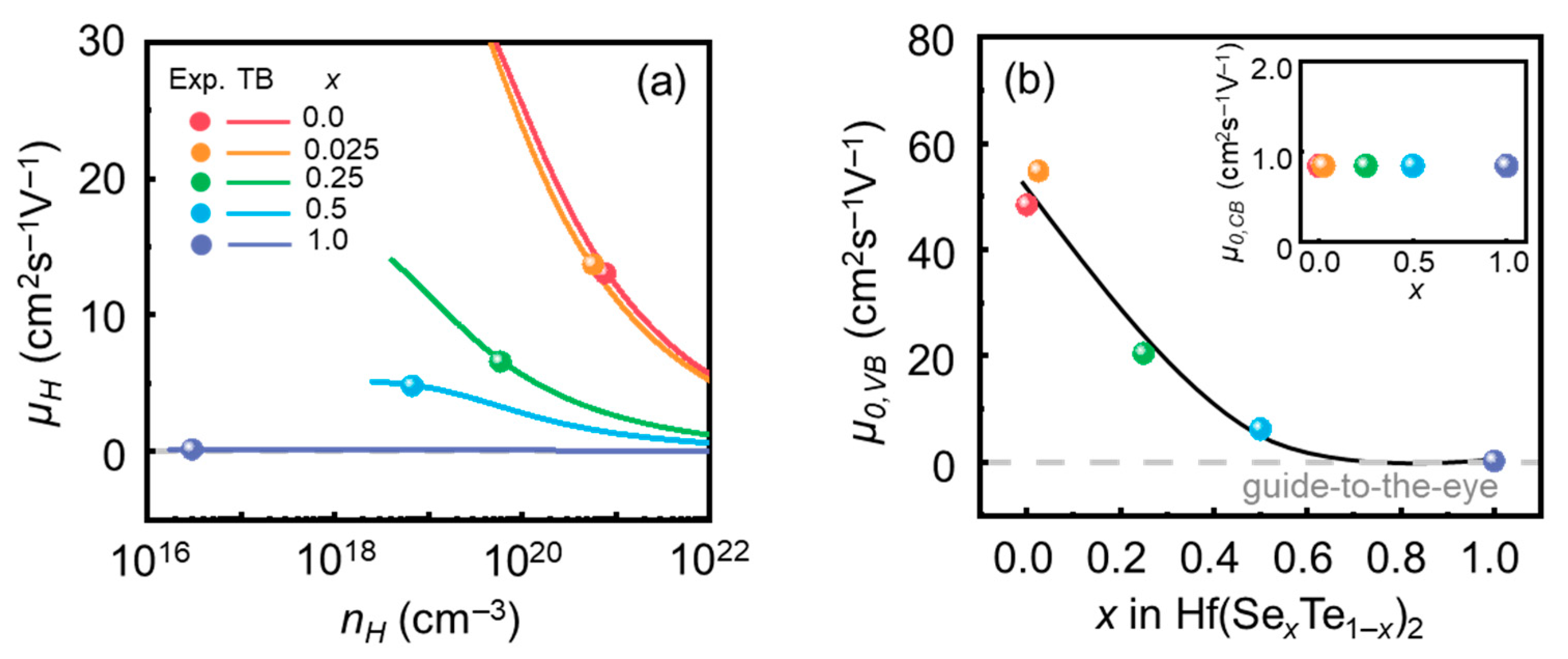
3.2. Estimation of the μ0,i (i = VB, CB) Via the TB Model

Figure 2a shows the experimental μH in terms of nH at 300 K adopted from Bang et al. (in symbols) [22]. The μH is substantially suppressed with increasing x. The μH of approximately ~13 cm2 V−1 s−1 for x = 0.0 and 0.025 is decreased down to 0.15 cm2 V−1 s−1 when x = 1.0. Because only the x = 0.0 and 0.025 samples have nH that are higher than 5 × 1020 cm−3 (other samples with x ≥ 0.25 have nH those are lower than 5 × 1019 cm−3), only the x = 0.0 and 0.025 samples have σ that are higher than 1200 S cm−1 (σ = e μH nH). The σ of the samples with x ≥ 0.25 are lower than 100 S cm−1 at 300 K [22]. In order to evaluate the characteristics of the electronic bands contributing to the electronic transport, we need to convert the μH into μ0. The μH is a function of μ0 and η, so depending on η, the trend observed in μH may not reflect the trend in the band parameter, μ0, which represents the carrier mobility without any defects. By fitting md,i* and μ0,i (i = maj, min) with different εg (Table 1) to the experimental μH in terms of nH by using the TB model, the lines in Figure 2a that accurately describe the experimental data (in symbols) are obtained. From the reasonable agreements between the experiments and the TB model results, we demonstrate that the band parameter μ0,i (i = maj, min) provided in Figure 2b describes the electronic bands well.
Figure 2b shows the μ0,VB (=μ0,maj) and μ0,CB (=μ0,min in the inset) of Hf(Te1−xSex)2 (x = 0.0, 0.025, 0.25, 0.5, and 1.0) estimated by using the TB model at 300 K. Again, to minimize any complications, the μ0,CB is kept constant for all different x (0.84 cm2 V−1 s−1). Overall, the μ0,VB decreases with increasing x. At first, the μ0,VB rapidly decreases with x, but for x > 0.25, the rate of the μ0,VB decrease decreases. The guide-to-the-eye is provided in the gray solid line. This suggests that increasing the Se alloying content deteriorates the mobility of the holes. The physical reason behind the μ0,VB reduction can be found by looking at how the carrier–phonon interaction changes with Se alloying. The μ0 of any band is related to the md* and deformation potential (Edef), as in Equation (15). The ħ and Cl in Equation (15) are the h/2π and the elastic constant, respectively.
μ 0 = ( 2 2 π 3 ) e 4 ( k B T ) 3 / 2 C l m d * 5 / 2 E d e f 2
As shown in Equation (15), the μ0 is inversely proportional to Edef2. The Edef quantifies how strong the scattering of charged carriers is due to lattice vibrations (phonons). If the Edef is high, this means that the charged carriers are more often scattered by phonons hindering the electronic transport properties. The Edef,VB (the Edef of the valence band) for different x are obtained from md,VB* (Figure 1b) and μ0,VB (Figure 2b), and are provided in Table 2. The general trend observed in Edef,VB is that the carrier–phonon interaction becomes stronger as x increases. However, it is to be noted that there is a local minimum in Edef,VB at x = 0.5.

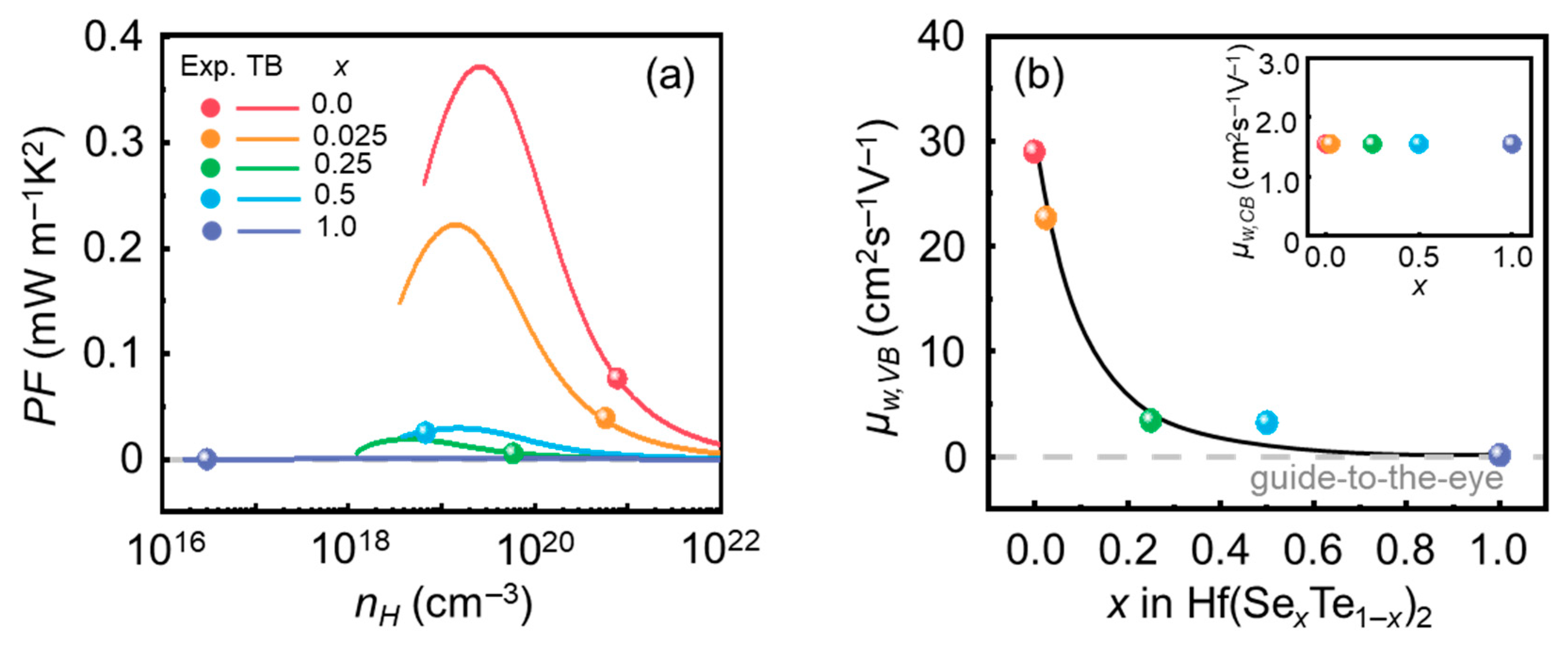
3.3. Estimation of the μW,i (i = VB, CB) Via the TB Model

Figure 3a shows the experimental power factor (= S2σ, PF) in terms of nH at 300 K adopted from Bang et al. (in symbols) [22]. The experimental PF decreases significantly with increasing x, except when x = 0.5. When x = 0.5 (PF = 0.025 mW m1 K2), the corresponding PF is approximately four times greater than that measured when x = 0.25 (PF = 0.006 mW m1 K2). However, when x = 1.0, its PF decreases to lower than 0.001 mW m1 K2. According to Figure 1a, the S of x = 1.0 (S = 730 μV K1) is much higher than those of other x. However, the μH of x = 1.0 is the lowest mostly due to high Edef (Table 2). The PF is a product between S2 and σ (= e μH nH). The large PF discrepancy between x = 0.0 and 1.0 is mostly due to the significant difference in nH (incorporated in σ). While the nH of x = 0.0 is in the order of 1021 cm3, that for x = 1.0 is only in the order of 1016 cm3. The factor of 105 difference cannot be offset, even with a large difference in the S. Based on the md,i* and μ0,i (i = VB, CB) estimated using the TB model (Figure 1b and Figure 2b), the PF in terms of nH are estimated for different x (Figure 3a in lines). Regardless of the x, the theoretical maximum PF are predicted near 1019 cm3, and the predicted maximum PF decreases significantly with increasing x. The theoretical maximum PF for x = 0.0 is as high as 0.37 mW m−1K2. Since the experimental PF for x = 0.0 is only 0.076 mW m1 K2, when the nH is tuned from 7.7 × 10²⁰ to 2.8 × 1020 cm3, an improvement of approximately 4.5 times in the PF is expected.
When there is only one band contributing to electronic transport, the theoretical maximum PF is directly proportional to the μW of the band. When there are two bands (valence and conduction bands) contributing, the theoretical maximum PF is related to the interplay between the μW,maj and μW,min. Out of the two band parameter, μW,maj would be more important when determining the theoretical maximum PF. Figure 3b shows the μW,VB and μW,CB (inset) of Hf(Te1−xSex)2 (x = 0.0, 0.025, 0.25, 0.5, and 1.0) at 300 K. Because we assume that the md,CB* and μ0,CB are invariant with x, corresponding μW,CB (Equation (13)) in terms of x (Figure 3b inset) is also independent to x. Generally, the calculated μW,VB decreases with increasing x. The values of μW,VB are approximately proportional to the theoretical maximum PF in Figure 3a. The values of μW,VB are not directly proportional to the theoretical maximum PF as the μW,CB values also contribute when determining the theoretical maximum PF. The contribution from μW,CB becomes larger for small x as the εg reduces for decreasing x (Table 1).

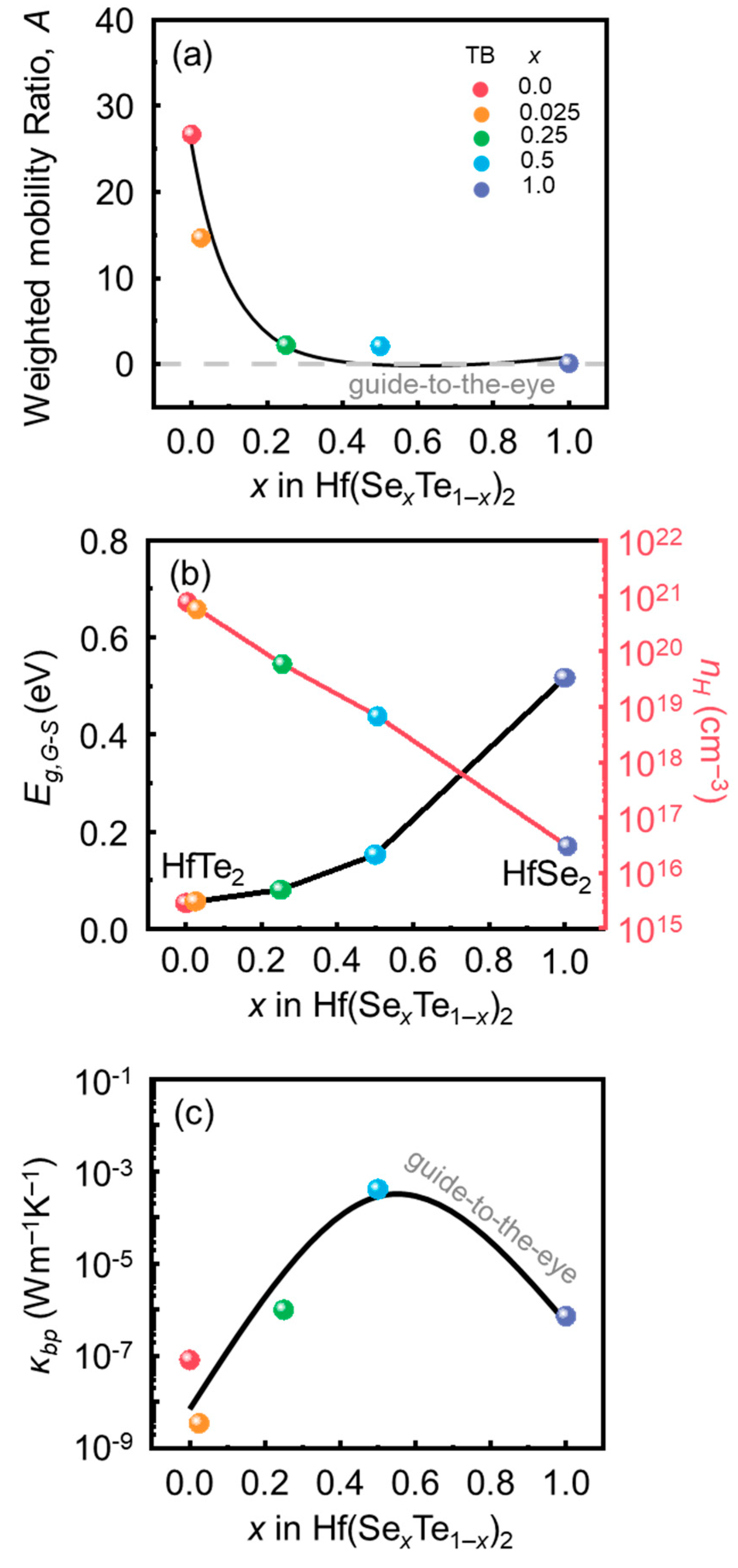
3.4. Estimation of the Bipolar Thermal Conductivity (κb) Via the TB Model

Figure 4a presents the theoretical weighted mobility ratio a computed using the μW,VB and μW,CB from Figure 3b. The A is defined as the ratio of μW,maj to μW,min (Equation (14)). Because Hf(Te1−xSex)2 (x = 0.0, 0.025, 0.25, 0.5, and 1.0) alloys are p-type, the A in Figure 4a is obtained by μW,VB divided by μW,CB. As we have kept the μW,CB constant for all x, the trend calculated in the A is almost identical to that observed in μW,VB. Similar to the μW,VB, the A rapidly decreases with increasing x. Except x = 0.0 and 0.025, the A of all x are smaller than 2.2. What A represents is how mobile majority carriers are with respect to the minority carriers. If A is much larger than one, it means that the majority carriers move much faster than minority carriers. In such a case, the bipolar contribution to electronic contribution weakens. Therefore, a much-suppressed bipolar conduction is expected when the A is large. According to Figure 4a, the samples with small x would experience much weaker bipolar conduction than those with large x. However, this only applies when other factors that affect the κb stay the same.
Figure 4b shows how the band gap estimated using the Goldsmid–Sharp equation (Eg,G-S) and the measured nH change in terms of x. The band gap and nH are also important factors that affect the κb. First of all, increasing the band gap will decrease the κb. Secondly, increasing nH will also decrease the κb. In Hf(Te1−xSex)2 (x = 0.0, 0.025, 0.25, 0.5, and 1.0) alloys, increasing x will increase Eg,G-S but decrease the nH at the same time. From Figure 4a,b, we now know that the increasing x will decrease A and nH, but increase Eg,G-S. We have two factors (A and nH) changing to increase the κb, and one factor (Eg,G-S) changing to suppress the κb with increasing x. The relative impact of each factor on κb is difficult to evaluate as those factors are strongly interdependent. Instead, the κb itself is estimated to see which factor affects bipolar conduction more strongly.
Figure 4c is the κb in terms of x estimated by using the TB model at 300 K. The κb is a function of Si, σi (i = maj, min), and T (Equation (16)). The Si and σi (i = maj, min) are defined as in Equations (2)–(3) and (5)–(6) [26,27,28,29,30,31,32,33].
κ b = [ σ m a j S m a j 2 + σ m i n S m i n 2 ( σ m a j S m a j + σ m i n S m i n ) 2 σ m a j + σ m i n ] T
According to Figure 4c, the κb increases with x until x = 0.5, and for x > 0.5 it starts to decrease. For small x, the Eg,G-S is also narrow. In such a circumstance, decreases in A and nH result in an increase in κb. However, once the Eg,G-S becomes wider than 0.15 eV (when x = 0.5), the effect of the band gap on bipolar conduction becomes much greater than those of A and nH. Hence, despite the decrease in A and nH, a reduction in κb is obtained with the band gap increase.

4. Conclusions

In summary, the electronic transport properties of p-type Hf(Te1−xSex)2 (x = 0.0, 0.025, 0.25, 0.5, and 1.0) alloys have been investigated in terms of electronic band parameters. Because the band gap of the Hf(Te1−xSex)2 alloys increases with increasing x, the Two-Band (TB) model (one valence band and one conduction band) has been adopted to take the band gap change into consideration. When we consider the majority carrier band (valence band in this case), its density-of-states effective mass first decreases but for x > 0.25, it increases again. The deformation potential increases with increasing x. Consequently, the weighted mobility and weighted mobility ratio of the valence band decrease with increasing x. The bipolar thermal conductivity is also estimated using the TB model. It peaks near x = 0.5 and decreases for x > 0.5. This trend observed in the bipolar thermal conductivity can be explained with the weighted mobility ratio, band gap, and carrier concentration change with increasing x. When the band gap is narrow (x < 0.5), the effects of the weighted mobility ratio and carrier concentration are strong, but when the band gap becomes wide (x > 0.5), the band gap becomes a more critical factor to bipolar conduction than the other two factors.

Author Contributions

Data curation, J.-Y.K.; Writing—original draft, S.-M.H. and S.-i.K.; Writing—review & editing, H.-S.K.; Visualization, M.H.; Supervision, H.-S.K. All authors have read and agreed to the published version of the manuscript.

Funding

This work was financially supported by the National Research Foundation of Korea (NRF), funded by the Ministry of Education (NRF-2021K2A9A1A06092290).

Institutional Review Board Statement

Not applicable.

Informed Consent Statement

Not applicable.

Data Availability Statement

The data presented in this study are available on request from the corresponding author.

Conflicts of Interest

The authors declare no conflict of interest.

References

  1. Petsagkourakis, I.; Tybrandt, K.; Crispin, X.; Ohkubo, I.; Satoh, N.; Mori, T. Thermoelectric materials and applications for energy harvesting power generation. Sci. Technol. Adv. Mater. 2018, 19, 836–862. [Google Scholar] [CrossRef] [Green Version]
  2. Tritt, T.M.; Subramanian, M.A. Thermoelectric Materials, Phenomena, and Applications: A Bird’s Eye View. MRS Bull. 2006, 31, 188–198. [Google Scholar] [CrossRef] [Green Version]
  3. Caballero-Calero, O.; Ares, J.R.; Martín-González, M. Environmentally Friendly Thermoelectric Materials: High Performance from Inorganic Components with Low Toxicity and Abundance in the Earth. Adv. Sustain. Syst. 2021, 5, 2100095. [Google Scholar] [CrossRef]
  4. Rosi, F.D. Thermoelectricity and thermoelectric power generation. Solid State Electron. 1968, 11, 833–868. [Google Scholar] [CrossRef]
  5. Liu, W.; Jie, Q.; Kim, H.S.; Ren, Z. Current progress and future challenges in thermoelectric power generation: From materials to devices. Acta Mater. 2015, 87, 357–376. [Google Scholar] [CrossRef] [Green Version]
  6. Snyder, G.J.; Toberer, E.S. Complex thermoelectric materials. Nat. Mater. 2008, 7, 105–114. [Google Scholar] [CrossRef] [Green Version]
  7. Lee, K.H.; Kim, Y.M.; Park, C.O.; Shin, W.H.; Kim, S.W.; Kim, H.S.; Kim, S.i. Cumulative defect structures for experimentally attainable low thermal conductivity in thermoelectric (Bi,Sb)2Te3 alloys. Mater. Today Energy 2021, 21, 100795. [Google Scholar] [CrossRef]
  8. Feng, Y.; Li, J.; Li, Y.; Ding, T.; Zhang, C.; Hu, L.; Liu, F.; Ao, W.; Zhang, C. Band convergence and carrier-density fine-tuning as the electronic origin of high-average thermoelectric performance in Pb-doped GeTe-based alloys. J. Mater. Chem. A 2020, 8, 11370–11380. [Google Scholar] [CrossRef]
  9. Kim, H.-S.; Heinz, N.A.; Gibbs, Z.M.; Tang, Y.; Kang, S.D.; Snyder, G.J. High thermoelectric performance in (Bi0.25Sb0.75)2Te3 due to band convergence and improved by carrier concentration control. Mater. Today 2017, 20, 452–459. [Google Scholar] [CrossRef]
  10. Hong, T.; Wang, D.; Qin, B.; Zhang, X.; Chen, Y.; Gao, X.; Zhao, L.-D. Band convergence and nanostructure modulations lead to high thermoelectric performance in SnPb0.04Te-y% AgSbTe2. Mater. Today Phys. 2021, 21, 100505. [Google Scholar] [CrossRef]
  11. Moshwan, R.; Liu, W.-D.; Shi, X.-L.; Wang, Y.-P.; Zou, J.; Chen, Z.-G. Realizing high thermoelectric properties of SnTe via synergistic band engineering and structure engineering. Nano Energy 2019, 65, 104056. [Google Scholar] [CrossRef]
  12. Wang, N.; Li, M.; Xiao, H.; Gao, Z.; Liu, Z.; Zu, X.; Li, S.; Qiao, L. Band degeneracy enhanced thermoelectric performance in layered oxyselenides by first-principles calculations. Npj Comput. Mater. 2021, 7, 18. [Google Scholar] [CrossRef]
  13. Dangić, Đ.; Hellman, O.; Fahy, S.; Savić, I. The origin of the lattice thermal conductivity enhancement at the ferroelectric phase transition in GeTe. Npj Comput. Mater. 2021, 7, 57. [Google Scholar] [CrossRef]
  14. Chhowalla, M.; Shin, H.S.; Eda, G.; Li, L.-J.; Loh, K.P.; Zhang, H. The chemistry of two-dimensional layered transition metal dichalcogenide nanosheets. Nat. Chem. 2013, 5, 263–275. [Google Scholar] [CrossRef] [PubMed]
  15. Muratore, C.; Varshney, V.; Gengler, J.J.; Hu, J.J.; Bultman, J.E.; Smith, T.M.; Shamberger, P.J.; Qiu, B.; Ruan, X.; Roy, A.K.; et al. Cross-plane thermal properties of transition metal dichalcogenides. Appl. Phys. Lett. 2013, 102, 081604. [Google Scholar] [CrossRef]
  16. Isomäki, H.; Boehm, J.v. Bonding and Band Structure of ZrS2 and ZrSe2. Phys. Scr. 1981, 24, 465. [Google Scholar] [CrossRef]
  17. Gaiser, C.; Zandt, T.; Krapf, A.; Serverin, R.; Janowitz, C.; Manzke, R. Band-gap engineering with HfSxSe2-x. Phys. Rev. B 2004, 69, 075205. [Google Scholar] [CrossRef]
  18. Bilc, D.I.; Benea, D.; Pop, V.; Ghosez, P.; Verstraete, J. Electronic and Thermoelectric Properties of Transition-Metal Dichalcogenides. J. Phys. Chem. C B 2021, 125, 27084–27097. [Google Scholar] [CrossRef]
  19. Ge, Y.; Wan, W.; Ren, Y.; Liu, Y. Large thermoelectric power factor of high-mobility transition-metal dichalcogenides with 1T’’ phase. Phys. Rev. Res. 2020, 2, 013134. [Google Scholar] [CrossRef] [Green Version]
  20. Bharadwaj, S.; Ramasubramaniam, A.; Ram-Mohan, L.R. Lateral transition-metal dichalcogenide heterostructures for high efficiency thermoelectric devices. Nanoscale 2022, 14, 11750–11759. [Google Scholar] [CrossRef]
  21. Yumnam, G.; Pandey, T.; Singh, A.K. High temperature thermoelectric properties of Zr and Hf based transition metal dichalcogenides: A first principles study. J. Chem. Phys. 2015, 143, 234704. [Google Scholar] [CrossRef] [PubMed] [Green Version]
  22. Bang, J.; Kim, H.-S.; Kim, D.H.; Lee, S.W.; Park, O.; Kim, S.-I. Phase formation behavior and electronic transport properties of HfSe2-HfTe2 solid solution system. J. Alloys Compd. 2022, 920, 166028. [Google Scholar] [CrossRef]
  23. May, A.F.; Snyder, G.J. Introduction to Modeling Thermoelectric Transport at High Temperatures. In Materials, Preparation, and Characterization in Thermoelectrics; CRC Press: Boca Raton, FL, USA, 2012; pp. 1–18. [Google Scholar]
  24. Goldsmid, H.J.; Sharp, J.W. Estimation of the thermal band gap of a semiconductor from seebeck measurements. J. Electron. Mater. 1999, 28, 869–872. [Google Scholar] [CrossRef]
  25. Gibbs, Z.M.; Kim, H.-S.; Wang, H.; Snyder, G.J. Band gap estimation from temperature dependent Seebeck measurement—Deviations from the 2e|S|maxTmax relation. Appl. Phys. Lett. 2015, 106, 022112. [Google Scholar] [CrossRef] [Green Version]
  26. Foster, S.; Neophytou, N. Effectiveness of nanoinclusions for reducing bipolar effects in thermoelectric materials. Com. Mat. Sci. 2019, 164, 91–98. [Google Scholar] [CrossRef] [Green Version]
  27. Graziosi, P.; Neophytou, N. Bipolar conduction asymmetries lead to ultra-high thermoelectric power factor. Appl. Phys. Lett. 2022, 120, 072102. [Google Scholar] [CrossRef]
  28. Hong, M.; Chen, Z.-G.; Yang, L.; Zou, J. Enhancing thermoelectric performance of Bi2Te3-based nanostructures through rational structure design. Nanoscle 2016, 8, 8681–8686. [Google Scholar] [CrossRef]
  29. Bahk, J.-H.; Shakouri, A. Enhancing the thermoelectric figure of merit through the reduction of bipolar thermal conductivity with heterostructure barriers. Appl. Phys. Lett. 2014, 105, 052106. [Google Scholar] [CrossRef]
  30. Burke, P.G.; Curtin, B.M.; Bowers, J.E.; Gossard, A.C. Minority carrier barrier heterojunctions for improved thermoelectric efficiency. Nano Energy 2015, 12, 735–741. [Google Scholar] [CrossRef] [Green Version]
  31. Muzaffar, M.U.; Zhu, B.; Yang, Q.; Zhou, Y.; Zhang, S.; Zhang, Z.; He, J. Suppressing bipolar effect to broadening the optimum range of thermoelectric performance for p-type bismuth telluride–based alloys via calcium doping. Mater. Today Phys. 2019, 9, 100130. [Google Scholar] [CrossRef]
  32. Parker, D.; Singh, D.J. Thermoelectric properties of AgGaTe2 and related chalcopyrite structure materials. Phys. Rev. B 2012, 85, 125209. [Google Scholar] [CrossRef] [Green Version]
  33. Zhang, L.; Xiao, P.; Shi, L.; Henkelman, G.; Goodenough, J.B.; Zhou, J. Suppressing the bipolar contribution to the thermoelectric properties of Mg2Si0.4Sn0.6 by Ge substitution. J. Appl. Phys. 2015, 117, 155103. [Google Scholar] [CrossRef] [Green Version]
Figure 1. (a) Experimental (symbols) and theoretical (lines) S in terms of nH for Hf(Te1−xSex)2 (x = 0.0, 0.025, 0.25, 0.5, and 1.0) at 300 K [22], (b) estimated md,VB* (=md* for holes) in terms of Se alloying content (x) at 300 K. The x-dependent md,CB* (=md* for electrons) at 300 K is provided in the inset.
Ceramics 06 00032 g001
Figure 2. (a) Experimental (symbols) and theoretical (lines) μH in terms of nH for Hf(Te1−xSex)2 (x = 0.0, 0.025, 0.25, 0.5, and 1.0) at 300 K [22], (b) estimated μ0,VB (=μ0 for holes) in terms of Se alloying content (x) at 300 K. The x-dependent μ0,CB (=μ0 for electrons) at 300 K is provided in the inset.
Ceramics 06 00032 g002
Figure 3. (a) Experimental (symbols) and theoretical (lines) power factor (PF) in terms of nH for Hf(Te1−xSex)2 (x = 0.0, 0.025, 0.25, 0.5, and 1.0) at 300 K [22], (b) estimated μW,VB (= μW for holes) in terms of Se alloying content (x) at 300 K. The x-dependent μW,CB (= μW for electrons) at 300 K is provided in the inset.
Ceramics 06 00032 g003
Figure 4. (a) Theoretical (symbols)-weighted mobility ratio a in terms of x for Hf(Te1−xSex)2 (x = 0.0, 0.025, 0.25, 0.5, and 1.0) at 300 K, (b) experimental (symbols) band gap estimated via Goldsmid–Sharp equation (Eg,G-S), and experimental (symbols) nH in terms of x at 300 K [22], (c) theoretical (symbols) bipolar thermal conductivity (κb) estimated for different x via the TB model at 300 K.
Ceramics 06 00032 g004
Table 1. The εg for Hf(Te1−xSex)2 (x = 0.0, 0.025, 0.25, 0.5, and 1.0) at 300 K [22].
x in Hf(Te1−xSex)2εg (Band gap/kBT)
0.02.06
0.0252.19
0.253.12
0.55.92
1.020.00
Table 2. The md,VB*, μ0,VB, and Edef,VB for Hf(Te1−xSex)2 (x = 0.0, 0.025, 0.25, 0.5, and 1.0) at 300 K.
x in Hf(Te1−xSex)2md,VB* (m0)μ0,VB (cm2 V−1 s−1)Edef,VB (eV)
0.00.948.390.051
0.0250.5954.780.081
0.250.2320.450.43
0.50.656.190.21
1.00.90.170.86
Disclaimer/Publisher’s Note: The statements, opinions and data contained in all publications are solely those of the individual author(s) and contributor(s) and not of MDPI and/or the editor(s). MDPI and/or the editor(s) disclaim responsibility for any injury to people or property resulting from any ideas, methods, instructions or products referred to in the content.

