1. Introduction
The technologies of laser sources in the mid-IR range have made noticeable progress over the past few decades. The most efficient mid-IR sources are solid-state lasers [
1], optical parametric oscillators (OPOs) [
2,
3,
4,
5], laser diodes [
6,
7], and quantum cascade lasers [
8]. High-power OPOs in the mid-IR range are currently represented by nonlinear optical crystals KTP, KTA, ZnGeP
2, GaSe, etc. [
9,
10,
11]. Since there are large Fresnel reflection losses for ZnGeP
2 R~25% (one side), antireflection coatings are necessary for its practical application [
12]. To significantly increase the efficiency of OPO, stringent requirements are imposed on the residual reflection and LIDT of such coatings.
The deposition of anti-reflection coatings is a complex and multi-stage process that includes many parameters. The method of deposition of optical films onto the substrate and the materials of coating are considered the fundamental parameters, especially in the manufacturing of laser optics operating in the IR range, where it is necessary to obtain high LIDT values.
Ion beam sputtering (IBS) [
13] is a deposition method of interference coating with a high LIDT value and dense films with a high-refractive index, which are also characterized by high LIDT values [
14,
15,
16,
17]. The IBS method mainly sputters a pure metal target (Ta, Nb, Al, etc.) by supplying the sputtering chamber with a reactive gas (oxygen) and their oxide targets (for example, Ta
2O
5, Nb
2O
5, Al
2O
3, etc.) [
14,
15]. The approaches described in [
17,
18] also make it possible to sputter sulfide and fluoride ceramic targets using the IBS method. In previous work [
18], the possibility of applying an optical anti-reflection coating with a high LIDT value on a ZnGeP
2 (hereinafter ZGP) substrate was presented. However, it has been shown that the specific sputtering rate of ZnS and YbF
3 by the IBS method is low [
18]; as a result, the sputtering process requires a long time, which causes a negative effect where pollutants and residual gas, in the volume of the sputter chamber, get into the anti-reflective coating, which can significantly affect LIDT. At the same time, in the operating range of the laser system, up to 5 μm, it is possible to use the low-refractive oxide material Al
2O
3 with ZnS, as shown in [
19]. However, the problem of low sputtering rate of high-refractive ZnS still persists.
Based on physical and chemical parameters, the most suitable material with similar characteristics to ZnS is zinc selenide (ZnSe). This material is actively used to create resonator windows and filters for systems operating in the range of 2–14 µm (material transparency region) [
20]. Additionally, there are practically few studies on sputtering this material and creating AR coatings from it. Basically, this material is sputtered by thermal evaporation from molybdenum boats [
21] and by the electron beam evaporation [
22]. There is information in the literature about the LIDT of ZnSe thin films. For example, in [
23], it is shown that its LIDT is in the range of 1–3 J/cm
2, at a pulse repetition rate of 1 Hz. At the same time, in [
24], an AR coating based on a ZnSe/YbF
3 pair shows LIDT at a level of 12.2 J/cm
2. Additionally, ZnSe/YbF
3 structures on CaF
2 substrates by the e-beam evaporation method obtained Bloch surface waves [
25] and deformable mirrors [
26]. The production of ZnSe/Al
2O
3 nanostructures and the study of their optical properties were conducted in [
27] by RF magnetron sputtering on single-crystal silicon. However, the above studies did not use the IBS method for ZnSe sputtering and the creation of an AR coating on its basis in a pair with oxide. Therefore, the aim of this work is to study and refine the modes of ZnSe sputtering by the IBS method, as well as to develop an optical anti-reflection coating for a ZGP single-crystal substrate with a high LIDT value and a high sputtering rate based on a pair of ZnSe/Al
2O
3 materials.
2. Substrate and Sputtering Equipment
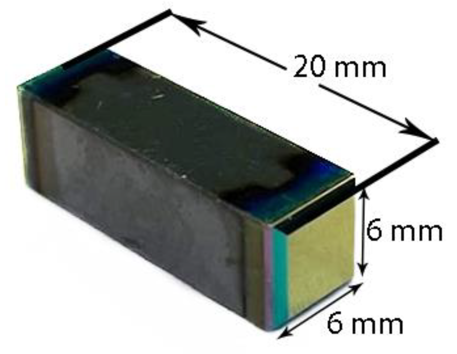
As a substrate, a ZGP single crystal with dimensions of 6 × 6 × 20 mm
3 (
Figure 1) was used, which was cut from a ZGP single-crystal boule (manufactured by LOC LLC, Tomsk, Russia) at angles θ = 54.5° and φ = 0° relative to optical axis. The ZGP single crystal boule was grown by the Bridgman method in the vertical direction on an oriented seed.
Working surfaces were polished by the technology described [
28]. The working surfaces of the samples were processed on a 4-PD-200 (Tomsk, Russia) polishing and finishing polish machine. Using this polishing machine, a laser quality polish was reached. The initial treatment of the working surfaces of all samples consisted of polishing on a cambric polishing pad using synthetic diamond powder DSF 0.5/0 (Diamond Synthetic Fine, average grain size 270 nm). In this case, the material removal was ~30 μm, which made it possible to remove the cracked layer formed in the process of cutting the crystal into oriented plates and their preliminary grinding—the polishing procedure. Next, the samples were polished on a cambric polishing pad using synthetic diamond powder DSF 0.25/0. Next, the samples were polished on a resin polishing pad made from polishing resin using DSF 0.25/0 synthetic diamond powder. The obtained samples were washed with cotton swabs and high purity acetone. Before applying interference coatings, the control of the profile of the working surfaces of the studied samples was carried out using a ZYGO NewView 7300 profilometer operating on the basis of white light interferometry. The polishing of all the elements under study was carried out in a block; therefore, to evaluate such parameters as the maximum difference in height and depth of inhomogeneities on the surface (Pz), RMS depth of roughness (Pa) was selected from one of the samples. Its surface areas of 110 × 90 μm in size were studied, which showed the following results: Pz = 31.372 nm, Pa = 0.442 nm (
Figure 2).
Before loading into the sputter chamber, the substrates were cleaned using high purity acetone and then washed with bidistilled water. An anti-reflection coating was applied to the polished surfaces of the sample using the IBS method.
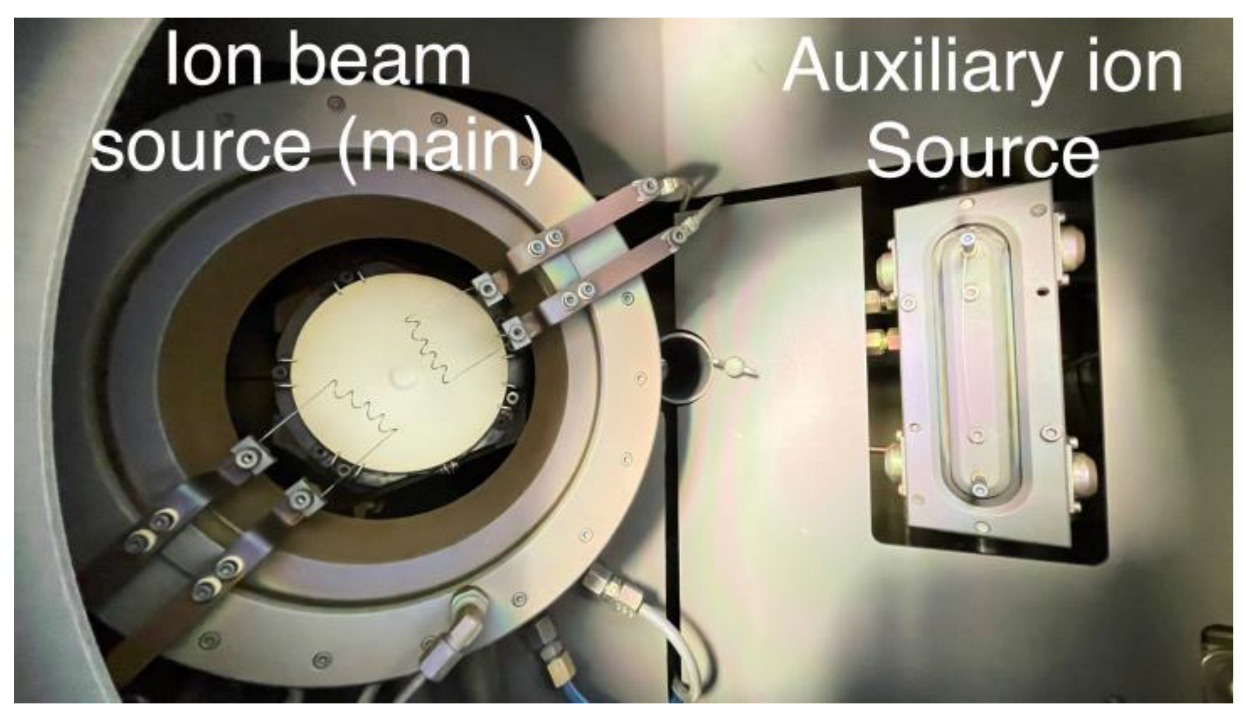
In this work, a vacuum-sputtering machine Aspira-200 manufactured by IZOVAC, Belarus, was used. The sputtering machine is equipped with an annular ion source (accelerator with anode layer), which has the ion-energy of 400–1500 eV (
Figure 3, left). The maximum voltage of the ion source reaches 4.5 kV. An auxiliary ion source with an ion-energy of 100–1000 eV and a maximum voltage of 3 kV was used for ion purification (~150 eV energy was chosen). By this source, the substrate surface was cleaned from contaminants directly inside the chamber before the deposition of the anti-reflection coating.
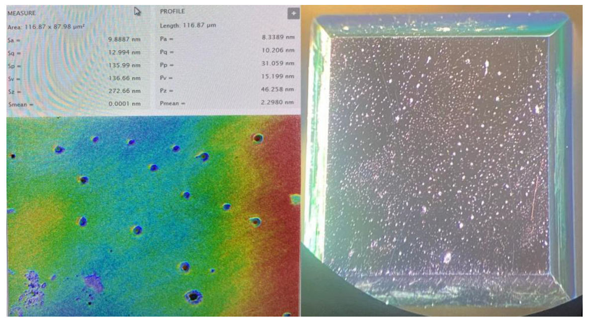
A series of experiments was also carried out to determine the modes of compensation of the ionic charge on the surface of the target and substrates. It was found that when the ratio of the discharge current to the emission current from the hot cathodes is 1/1.3 (the emission current of the hot cathodes is 30% higher than the discharge current), the ion charge is completely compensated. When deviating from the obtained ratio, we observed the following: when the ionic charge was undercompensated, defective structures of breakdowns by uncompensated heavy argon ions appeared in the film, and when overcompensated, an electronic breakdown of growing films occurred with the appearance of a “starry sky”-type defect, recorded with a profilometer (
Figure 4, left) and an optical microscope (
Figure 4, right).
The deposition equipment provides heating for the substrate up to 300 °C. However, during the deposition process, the substrate temperature was maintained at 100 °C. It was impossible to use higher temperatures due to the limitation imposed by the substrate because at temperatures above 100 °C, annealing of the material and damage to optical characteristics may occur. High-purity argon (AR 99.995%) was chosen as the working gas. The sputtering targets were disks with a diameter of Ø101.6 mm and a thickness of 6 mm. A ZnSe single-crystal target with a purity of 99.999% (5N), manufactured by Electrosteklo LLC, Russia, was chosen as a high-refractive material. An Alumina metal target with a purity of 99.999% (5N), produced by Xing Kang coating materials, China, was chosen as a low-refractive material.
3. AR Coating Design
To develop AR coating, firstly, single layers of materials, from which we later developed an interference coating, were studied. ZnSe was used as a high-refractive layer, and Al
2O
3 was used as a low-refractive layer. The deposition parameters of the studied materials are presented in
Table 1.
The selection of spraying modes was carried out using electronic gas flow meters, as well as accelerating voltage at the source. The optimal ratios of the Ar/O
2 gas mixture for the Al
2O
3 monolayer were selected, at which a low optical absorption was observed in the studied samples, and a high sputtering rate and film density were achieved (determined from the change in the refractive index). Only argon gas was used to sputter the ZnSe target. Thus, we obtained the following gas regimes for the materials under study, presented in
Table 1.
With such configurations of gas supply and voltages, an optimal ratio of the deposition rate to the quasi-stoichiometry of the film composition (determined indirectly, by the refractive index), its adhesion to the substrate, and mechanical strength were observed. In the case of oxide materials, a change in the Ar value in the gas mixture led to an increase in the optical absorption in the films. An increase in O2 in the mixture led to a significant (up to 2 times) decrease in the sputtering rate due to the “acidification” of the target and the formation of an oxide film on its surface.
As can be seen from
Table 1, the rate of deposition of the Al
2O
3 layer is about 0.1 nm/s, which is approximately 5 times higher than the rate of deposition of the YbF
3 layer (equal to 0.02 nm/s [
18]) when targets were sputtered by the IBS method. The sputtering rate of the high-refractive ZnSe material was ~0.09 nm/s, twice as high as ZnS, the sputtering rate of which is 0.04–0.045 nm/s [
18]. Thus, the time of sputtering process can be significantly reduced using Al
2O
3 instead of YbF
3, where possible, and ZnSe instead of ZnS.
Next, the dispersion characteristics of used materials was obtained. The refractive index dispersions, as well as the absorption of the layers, were calculated in the Optichar software module version 14.57 of the Optilayer software. The calculation was carried out according to the transmission and reflection characteristics of the layers under study deposited on BK8 optical glass (in the wavelength range of 400–2000 nm) and a germanium plate to describe them in the IR region. The thickness of the deposited single layers was about 1 μm. The transmission and reflection spectra were obtained using a Shimadzu UV-3600 Plus spectrometer (Shimadzu, Japan, Tokyo) and a Simex FT-801 Fourier spectrometer (Novosibirsk, Russia).
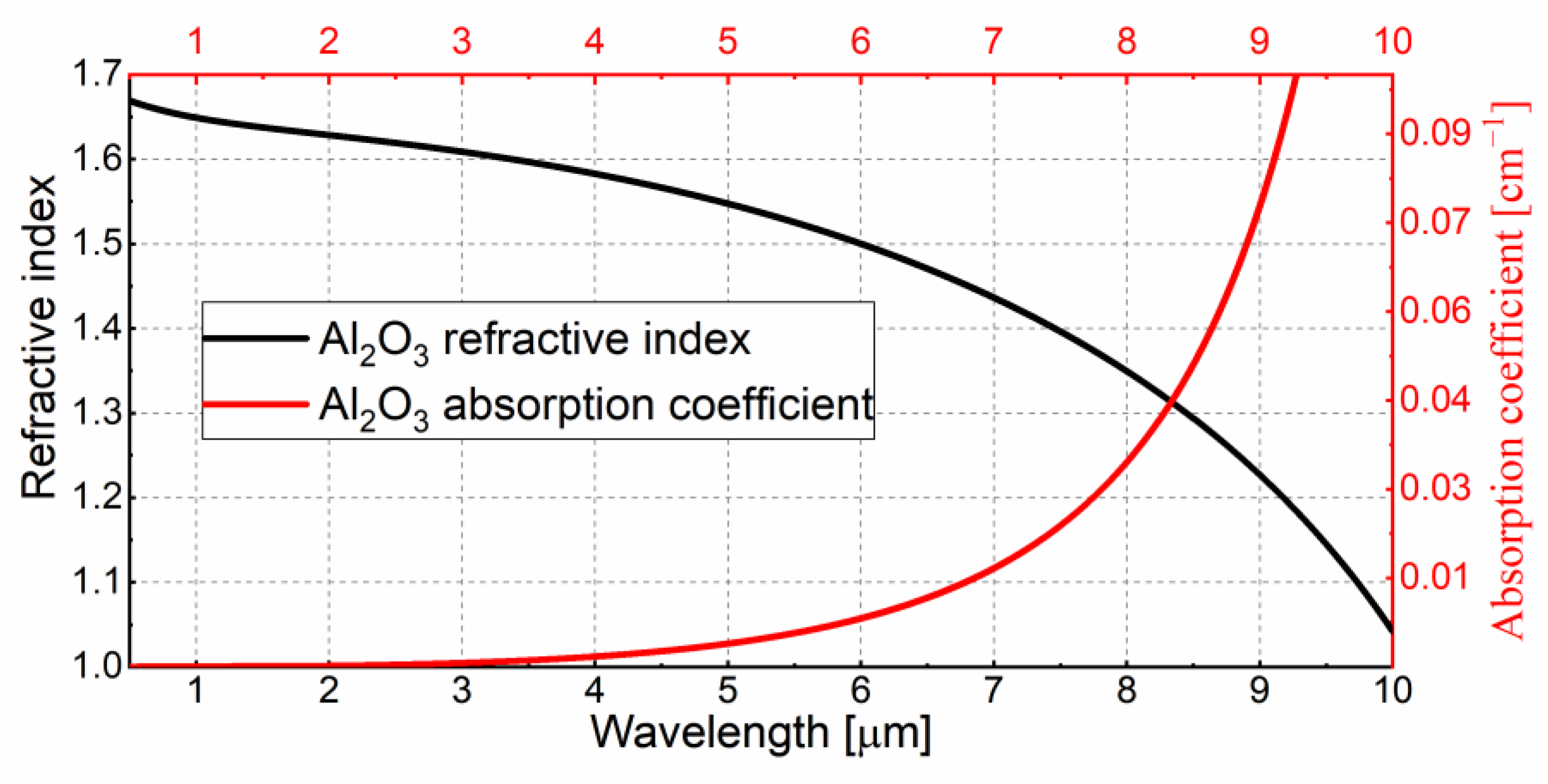
Figure 5 shows the refractive index dispersion and absorption of an Al
2O
3 single layer.
The refractive index dispersion of Al
2O
3 changes slightly by Δn~0.15 in the visible wavelength range up to 6 μm. At the same time, in the range of wavelengths longer than 6 μm, a rather sharp decrease in the refractive index and a sharp increase in absorption are observed. This is due to the presence of a wide resonant absorption line in the range of 10–12 µm, due to the presence of M–O bonds [
29]. Therefore, aluminum oxide can be used in the production of optical coatings operating in the IR range up to ~6 µm, and in relatively thin layers, less than ≤1 µm thick.
Then, the optical properties of the ZnSe single layer were determined. The refractive index dispersion is shown in
Figure 6.
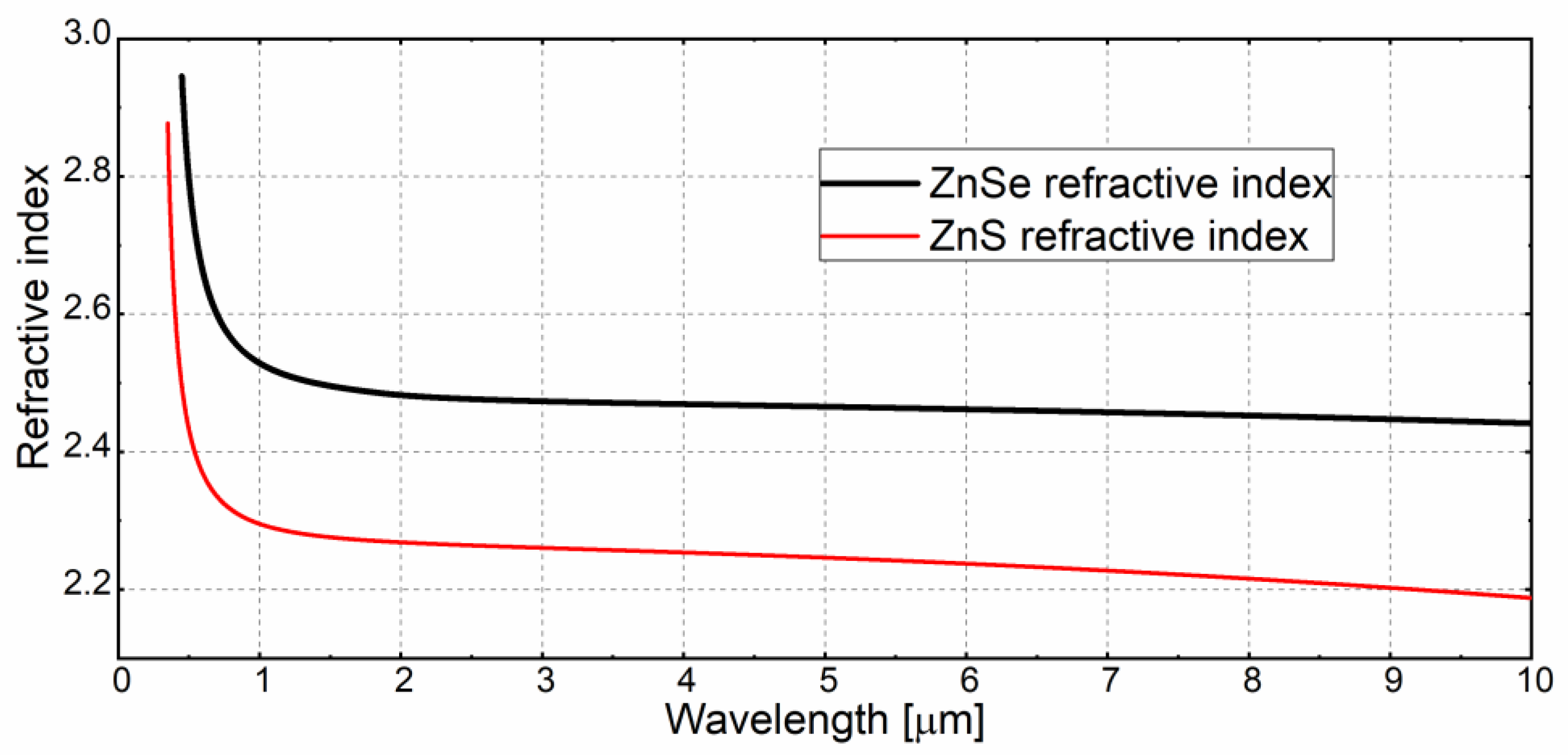
According to the obtained dispersion, the refractive index of ZnSe changes slightly by Δn ≤ 0.1 in the range from 1.5 µm to 12 µm wavelengths. The sharp increase in the refractive index is associated with the presence of resonant absorption bands in the range of 250–270 nm [
20]. This material is practically transparent in the range from 800 nm to 15–16 µm. The absorption of a single layer is not shown in
Figure 4 because it is not informative, as it is close to zero (α ≤ 10
−6 cm
−1) in the range of 1–12 µm. It should also be noted that the refractive index agrees well with the obtained data in [
30]. As shown in
Figure 4, the difference in refractive index dispersions for ZnSe and ZnS layers is Δn ≥ 0.2.
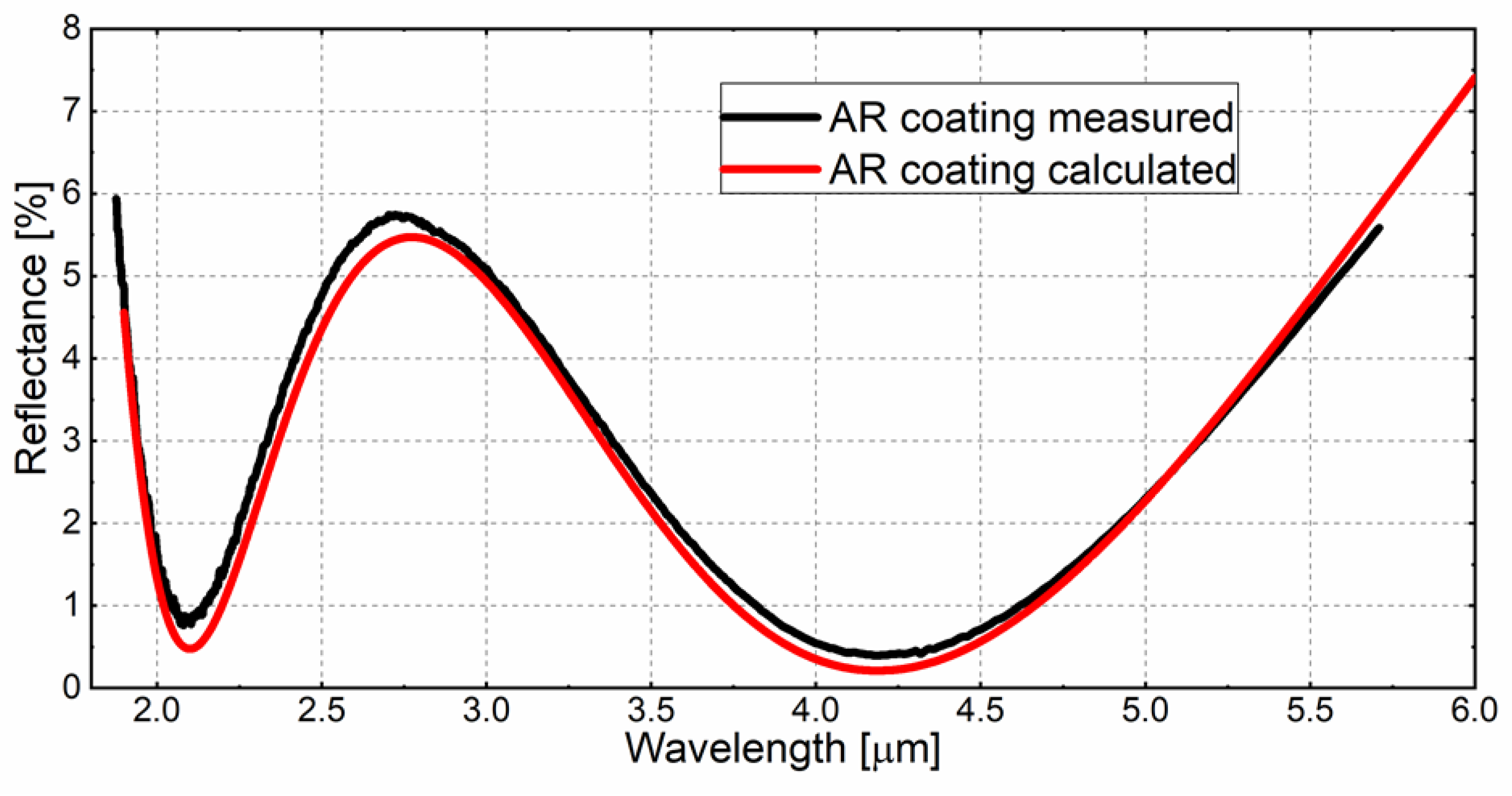
Using the obtained optical characteristics of the materials, a three-layer AR coating was calculated for the ZGP substrate according to the scheme sub│0.94 L 2.69 H 5.23 L│air, where L is the low-refractive layer, H is the high-refractive layer, and sub is the ZGP substrate. A control wave of 600 nm was chosen. An incident angle of 0⁰ was chosen and an average polarization Ra was used. The operating band of the coating was chosen to generate OPO on ZGP in the range of 3500–5000 nm, pumped with 2097 nm of radiation. The calculated coating was deposited on a ZGP single crystal (
Figure 1), and on a ZGP control plate, one of its sides was matte. The characteristics of the calculated and measured coating, as well as its spectra, are presented in
Table 2 in
Figure 7.
As can be seen from
Figure 7, the measured reflection spectrum of the AR coating has some differences from the calculated one. This is due to the presence of residual reflection from the matted surface of the substrate and the error in determining the refractive index dispersion, in addition to the error in the layer thickness during deposition, which occurs due to the lack of a quartz sensor for measuring the thickness of the sputtered layer inside the chamber, The control of the sputtered coating was carried out by optical transmission methods.
The obtained coating satisfies the target characteristics indicated in
Table 2. Using ZnSe instead of ZnS allowed us to reduce the thickness of the high-refractive layer by 65%, from 264 nm to 154 nm, while maintaining the optical characteristics of the coating, with a slight change in the thicknesses of the low-refractive layer. This reduced the deposition time from 5 to 3 h, that is, by ~30%. The LIDT of the obtained coating on the ZGP substrate was tested using a Ho:YAG laser The measurement results are shown below.
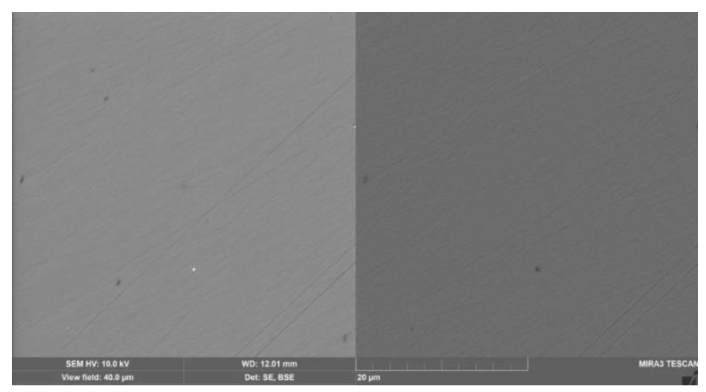
During the work, the morphology of the deposited interference coating was determined on a Tescan MIRA 3 LMU scanning electron microscope with a Schottky cathode. Scanning was performed at an accelerating voltage (HV) of 10 kV. The samples were coated with a carbon conductive coating using a Quorum Technologies EMITECH K450X setup (Quorum Technologies, Laughton, UK). As studies have shown, in the sample, in the layers of defects in the interference antireflection coating, no defective structure of the film was found; only defects in the surface layer of the substrate, scratches and dents after polishing, shown in
Figure 8, were found.
4. LIDT Test of AR-Coated OPO
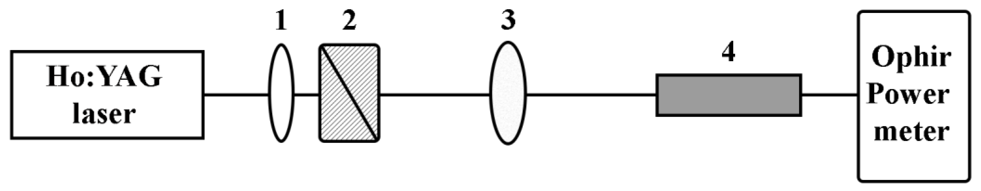
The block-scheme of the laser system used in the experiment in the LIDT test in
Figure 9 is shown. The Ho:YAG laser with a wavelength of 2097 nm, pulse repetition rate of 10 kHz, pulse duration of 35 ns, and with p-polarization was used. The measured diameter of the laser beam on the input crystal surface was d = 350 µm at the e
−2 level of the maximum intensity in all experiments. The maximum average radiation power generated by the Ho:YAG laser was 20 W in a linearly polarized Gaussian beam (parameter M
2 ≤ 1.3). The output laser power could be controlled by the system of the polarizer (1) and BSC (2) by the rotation of polarizer (1).
To determine the LIDT of the investigated samples, the “R-on-1” method was used according to the ISO standard described in detail in [
10,
11], which requires less space on the sample surface compared to the “S-on-1” method and, therefore, can be applied to samples with a limited aperture, but is considered more rough. The essence of this technique lies in the fact that each individual region of the crystal is irradiated with laser radiation with a successive increase in the intensity of laser radiation until an optical breakdown occurs or a predetermined energy density value is reached. In our work, the study was carried out with an exposure duration of laser radiation τ
ex = 10 s. The sample under study was exposed to packets of laser pulses with a fixed level of energy density that did not cause damage to the surface of the crystals. Further, the energy density level increased with a step of ~0.1 J/cm
2. When visible damage appeared on one of the surfaces of the nonlinear element, the experiment was terminated. Then, the sample was moved by 0.8 mm in height or width using a two-coordinate shift. The experiment was repeated 10 times. The optical breakdown probability was obtained by plotting the cumulative probability as a function of the optical breakdown energy density. The value of LIDT (W
0) was taken to be the energy density corresponding to the leading approximation of the probability of optical breakdown to zero.
Three samples were tested: (1) without AR coating; (2) with AR coating ZnS/Al
2O
3; (3) with AR coating ZnSe/Al
2O
3. The measurement results are shown in
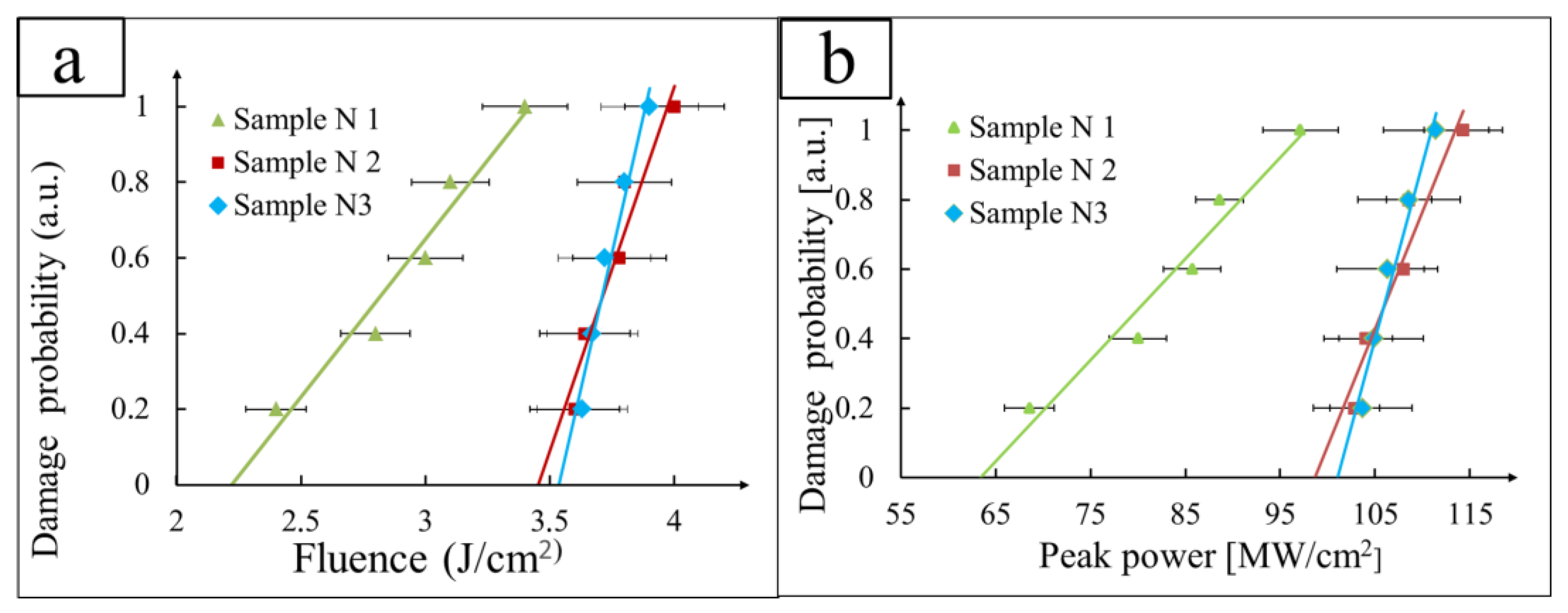
Figure 10. The measurements were carried out on a sample of 10 points for each sample, and the statistical error in determining the LIDT value is also given. Damage (crystal breakdown) was recorded by a sharp drop in the radiation power on the power meter, as well as by the glow of ionized ejection products from the surface and a characteristic sound. Then, the damage to the surface was fixed in an optical microscope. In the graphs presented, the ordinate shows the probability of optical breakdown in relative units, normalized to unity, and the abscissa shows the energy density of the testing laser radiation.
Thus, the LIDT of sample No. 1 (without antireflection coatings) was
= 2.23 J/cm
2 and
= 64 W/cm
2, where
is LIDT in energy density and
is expressed in power density. The LIDT of sample No. 2 (ZnS/Al
2O
3) was
= 3.45 J/cm
2 and
= 99 W/cm
2. The optical breakdown threshold of sample No. 3 (ZnSe/Al
2O
3) was
= 3.51 J/cm
2 and
= 101 W/cm
2. As in our previous work [
11], an increase by 1.5 times in LIDT was observed after the deposition of antireflection coatings based on ZnSe and Al
2O
3 materials. The selected pairs of materials have physicochemical properties that promote good adhesion of the multilayer coating to the polished crystal surface and minimal mechanical stresses between the layers and at the substrate/film interface, which, as a result, leads to an increase in LIDT. An adhesion test was carried out using ISO 9211-4:2012 “Optics and photonics-Optical coatings-Part 4: Specific test methods”.

 ,
, 


