Article

Estimation of Temperature-Dependent Band Parameters for Bi-Doped SnSe with High Thermoelectric Performance

Department of Materials Science and Engineering, University of Seoul, 163 Seoulsiripdae-ro, Seoul 02504, Republic of Korea
*
Author to whom correspondence should be addressed.
These authors contributed equally to this work.
Ceramics 2023, 6(1), 504-513; https://doi.org/10.3390/ceramics6010029
Submission received: 17 December 2022 / Revised: 9 February 2023 / Accepted: 9 February 2023 / Published: 13 February 2023
(This article belongs to the Special Issue Thermoelectric Properties of Ceramic-Based Materials)

Abstract

:
Recent studies have revealed the outstanding thermoelectric performance of Bi-doped n-type SnSe. In this regard, we analyzed the band parameters for Sn1−xBixSe (x = 0.00, 0.02, 0.04, and 0.06) using simple equations and the Single Parabolic Band model. Bi doping suppresses the carrier-phonon coupling while increasing the density-of-states effective mass. The n-type SnSe is known to have two conduction bands converge near 600 K. Bi doping changes the temperature at which the band convergence occurs. When x = 0.04, its weighted mobility maximized near 500 K, which indicated the possible band convergence. The highest zT of the x = 0.04 sample at mid-temperatures (473–573 K) can be attributed to the engineered band convergence via Bi doping.

1. Introduction

Research on various eco-friendly energy technologies has been conducted in various fields to mitigate the acceleration of global warming [1]. In particular, environmentally friendly energy harvesting technologies can play an important role in reducing greenhouse gas emissions, which are a main cause of climate change. Among many environmentally friendly technologies that can harvest energy without consuming fossil fuels, thermoelectric technology is drawing increasing attention because it can convert waste heat into electricity [2]. The conversion efficiency (from waste heat to electricity) of the device is closely coupled with the thermoelectric performance of a material used in the device. The thermoelectric performance of a material is evaluated with a figure of merit, zT, which is defined as zT = S2σT/(ĸe + ĸl), where S, σ, T, ĸe, and ĸl are the Seebeck coefficient, electrical conductivity, absolute temperature, electronic thermal conductivity, and lattice thermal conductivity, respectively. Here, the S2σ, termed as the power factor, determines the electronic transport properties of the material [3]. As evident from the equation, a high zT can be achieved by using a material with a high power factor and low thermal conductivity. However, enhancing the power factor is not simple. The S and σ move in the opposite direction when the carrier concentration of a material is controlled with doping or alloying [4,5,6,7,8,9,10,11,12]. Commonly, several band engineering strategies have been introduced to decouple the trade-off relationship between the S and σ [13,14,15,16,17]. At the same time, materials with an inherently high power factor have been sought.
Kutorasinski et al. found that SnSe, a layered material, has highly anisotropic hole transport properties. Their study showed that p-type SnSe cannot transport charged carriers (holes) in the interlayer, whereas n-type SnSe can do so, thus yielding higher thermoelectric performance. Consequently, n-type SnSe is a better thermoelectric material, owing to its high power factor [4]. Recently, Duong et al. reported n-type Bi-doped SnSe with a maximum zT of 2.2 at 773 K with a high power factor while maintaining a low thermal conductivity [18]. They synthesized Bi-doped SnSe (Sn1−xBixSe; x = 0, 0.02, 0.04, and 0.06) and experimentally demonstrated that the power factor of the x = 0.04 sample improved by more than a factor of eleven compared to the pristine SnSe (x = 0) at 572 K. Moreover, an exceptionally high zT of 2.2 was obtained in the x = 0.06 sample at 773 K. Because the total thermal conductivities (ĸe + ĸl) of the x = 0.04 and 0.06 samples are similar, their zTs are closely related to their power factors. With a changing Bi doping content (x), the corresponding σ changed more significantly than their S did. However, the effect of Bi doping on electronic band parameters of Sn1−xBixSe was not provided.
Here, we estimate the band parameters, namely, the density-of-states effective mass (md*), non-degenerate mobility (μ0), weighted mobility (μW), and B-factor of Sn1−xBixSe (x = 0, 0.02, 0.04, and 0.06) using the single parabolic band (SPB) model. From how the band parameters change with different Bi doping content, we evaluate the impact of Bi doping on the electronic transport properties of Bi-doped SnSe. At 300 K, Bi doping first decreases the μW, which is directly proportional to the theoretical maximum power factor; however, when the x = 0.06, the μW is improved by more than a factor of five compared to the pristine SnSe. A drastic increase in the 300 K power factor of the x = 0.06 sample is predicted. The 300 K μW improvement is mostly due to the md* increase with Bi doping, despite the substantial drop in the μ0.

2. Materials and Methods

Temperature-dependent S and Hall carrier concentration (nH) were obtained from the literature [18]. The experimental S and nH, both measured at 300 K, were used to plot the S as a function of nH. The nH was converted to chemical carrier concentration (n) using Equation (1) [19].
n n H = 1.17 0.216 1 + exp S 101 67.1
The experimental n-dependent S at 300 K was converted to S-dependent log10(n) to estimate the md*. The md* of each sample was estimated by fitting Equation (2) into the experimental data expressed as S-dependent log10(n) [20].
log 10 m d * T 300 = 2 3 log 10 n 2 3 20.3 0.00508 × S + 1.58 × 0.967 S
Temperature-dependent μ0 was estimated from the experimental nH-dependent μH at different temperatures using the Single Parabolic Band (SPB) model [21,22]. According to the SPB model under acoustic phonon scattering, the μH is defined in terms of μ0 and reduced fermi level η (Equation (3)).
μ H = μ 0 F 1 / 2 η 2 F 0 η
The fermi integral of order i (Fi) in Equation (3) is defined as in Equation (4).
F n η = 0 ε n 1 + exp ε η d ε
The nH is defined in terms of md* and η (Equation (5)).
n H = 16 π 3 2 m d * k B T h 2 F 0 η 2 F 1 / 2 η
Equations (3)–(5) were applied to the experimental nH-dependent μH to estimate μ0. The temperature-dependent μW was calculated using Equation (6) [23].
μ w = 3 h 3 σ 8 π e 2 m e k B T 3 / 2 exp S k B / e 2 1 + exp 5 S k B / e 1 + 3 π 2 S k B / e 1 + exp 5 S k B / e 1
The e, me, h, and kB are the electric charge, electron rest mass, Planck constant, and Boltzmann constant, respectively. Finally, the B-factor is estimated using the μW and the lattice thermal conductivity (κl), as in Equation (7).
B = k B e 2 8 π e 2 m e k B 3 / 2 h 3 μ W T 5 / 2 κ l

3. Results and Discussion

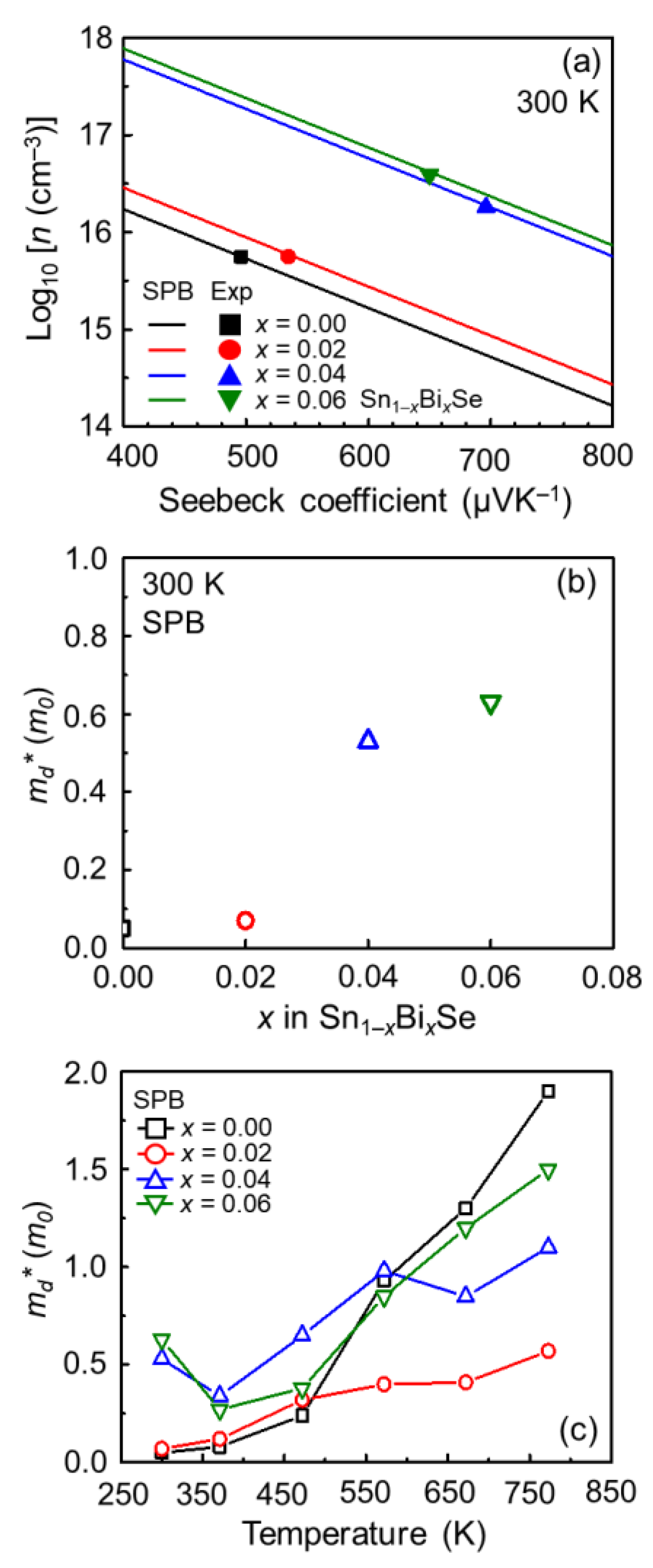
3.1. Calculation of Density-of-States Effective Mass, md*

Figure 1 shows the calculated md* for Sn1−xBixSe (x = 0.00, 0.02, 0.04, and 0.06). Figure 1a shows the experimental |S|and nH for varying x at 300 K expressed in log10(n) versus |S| graph (in filled symbols). Because we could not measure the n directly, the measured nH was converted to n using Equation (1) [19]:
The ratio of n to nH is a Hall factor (rH), and it is a function of η (reduced fermi level). Because the S is determined by the η mathematically according to the SPB model, the rH can also be expressed in terms of S instead of η. That is the reason why the rH in Equation (1) is expressed in terms of S. The conversion from the nH-dependent S to the S-dependent log10(n) is necessary to accurately estimate the md* from it. The simple and accurate equation that enabled us to calculate the md* without having to worry about solving the fermi integrals in the SPB model numerically (Equation (4)) was expressed in terms of S and log10(n), as shown in Equation (2) [20].
When the T, n, and S in units of K, cm−3, and μV K−1 are inserted into Equation (2), the md* in the unit of me is obtained. While varying S from 400 to 800 μV K−1, the md* in Equation (2) is fitted to describe the experimental data in the filled symbols. The results of fitting md* using Equation (2) are presented in lines in Figure 1a. From the fact that the filled symbols are on top of the lines of the same color, we can conclude that the fitted md* accurately represents the electronic band structure of the samples. From the experimental data (filled symbols), we can see that the n increases with increasing Bi doping content (x). However, the S only increases up to x = 0.04. The S of the x = 0.06 sample is lower than that of the x = 0.04 sample. It is to be noted that the x = 0.00 sample is p-type, while Bi-doped SnSe samples are all n-type. Figure 1b shows the 300 K md* for different x. In general, the md* increases with an increasing x. The rate of md* increase is the most abrupt when the x increases from 0.02 to 0.04, but the md* increases from x = 0 to 0.02 or from x = 0.04 to 0.06 are not substantial. As the x increases from 0 to 0.06, the calculated md* increases from 0.05 to 0.63 me (increasing by more than a factor of twelve). When we assume that there is only one band contributing to the electronic transport properties of Sn1−xBixSe (x = 0.00, 0.02, 0.04, and 0.06), the curvature of the band substantially increases with Bi doping at 300 K. How the md* changes with temperature may also be affected by the amount of x. Figure 1c shows the temperature-dependent md* for different values of x. Although the md* of the x = 0.00 sample is the lowest among other x values at 300 K, it becomes the highest at 773 K. The rate of md* change with temperature is different for different x values. Except for the x = 0.00 sample, the rate of md* increase increases with an increasing x. Although varying in degree, local peaks are observed near 550–650 K for all x. This can be attributed to the two conduction bands converging near 600 K [24]. Because the two conduction bands converging near 600 K are calculated for n-type SnSe, Bi doping can alter the temperature at which the two conduction bands converge and even the curvature of the two bands. Because we employed the SPB model (only one band contributing to transport), if band convergence occurs, it will be reflected as an increase in the md* of the assumed single band.

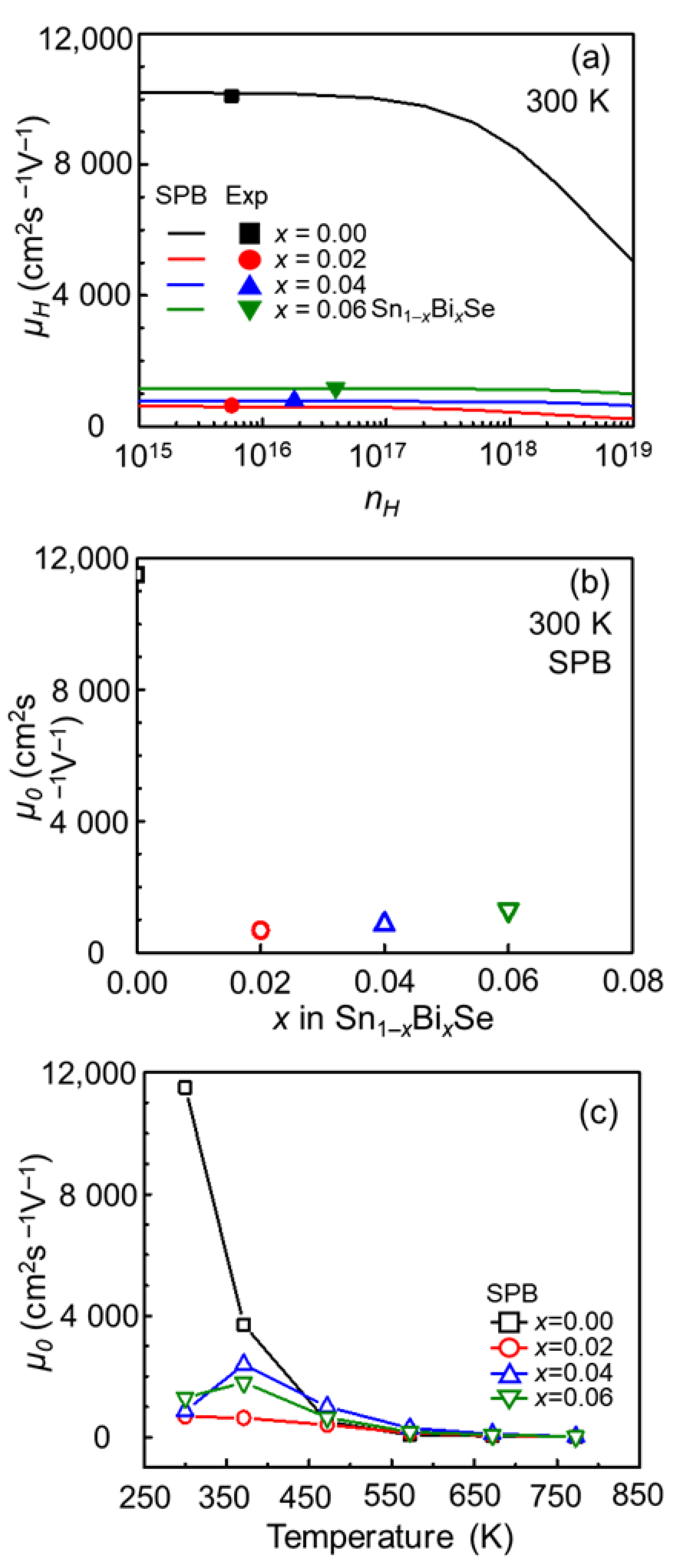
3.2. Calculation of Non-Degenerate Mobility, μ0

Figure 2a shows the calculated (lines) and experimental (filled symbols) nH-dependent μH for Sn1−xBixSe (x = 0.00, 0.02, 0.04, and 0.06) at 300 K [18]. The nH-dependent μH calculated using the SPB model (denoted by lines) are in agreement with the experimental data (filled symbols) when the μ0 is fitted accurately. According to the SPB model, the μH and nH are defined in Equations (3)–(5) [21,22].
To calculate nH-dependent μH, two band parameters needed to be determined: μ0 (Equation (3)) and md* (Equation (5)). By substituting the md* we obtained in Figure 1c into Equation 5, only the μ0 could be estimated by fitting Equations (3)–(5) to the experimental data (filled symbols). The μH of the x = 0.00 sample is approximately a factor of 10 greater than those of the Bi-doped samples. When Bi is doped to the x = 0.00 sample, the type of the sample changes from p- to n-type. Once Bi is doped, increasing x also increases the μH and nH, at the same time. The estimated μ0 at 300 K is shown in Figure 2b. Similar to μH, the μ0 rapidly decreases as Bi doping commences, and subsequently increases with an increase in x. As the Bi-doping concentration, x, increases from 0 to 0.06 in steps of 0.02, μ0 is calculated to be 11,500, 680, 860, and 1300 cm2 s−1 V−1, respectively. The μ0 is always higher than μH, because it represents the μH without defects at low degeneracy. The μ0, in turn, depends on single band mass (related to md*) and deformation potential (related to carrier-phonon interaction). The heavier the band mass, the lower the μ0. If the deformation potential is high, corresponding μ0 will be low. Because Bi doping increases the md* at 300 K (Figure 1b), from the fact that Bi doping also increases the μ0 at 300 K (Figure 2b) we can suggest that the interaction between the charged carriers and the phonons decreases with Bi doping at 300 K (favorable to electronic transport). The estimated μ0 with temperature is plotted in Figure 2c. The increasing carrier-phonon scattering at high temperatures and the md* (Figure 1c) are responsible for the drop in μ0 with temperatures. Among Bi-doped samples, unlike the x = 0.02 sample whose μ0 decreases with temperatures, the μ0 of x = 0.04 and 0.06 samples peak near 373 K. With the exception of 300 and 773 K, the μ0 of x = 0.04 are higher than those of the x = 0.06 sample at all temperatures. Different trends observed in the temperature-dependent μ0 can be understood in terms of how the md* and deformation potential of the samples change with temperatures. At 773 K, SnSe has the lowest μ0 of 6.4 cm2 s−1 V−1, whereas Sn1−xBixSe, with x = 0.02, 0.04, and 0.06, have μ0 of 13, 21, and 22 cm2 s−1 V−1, respectively.

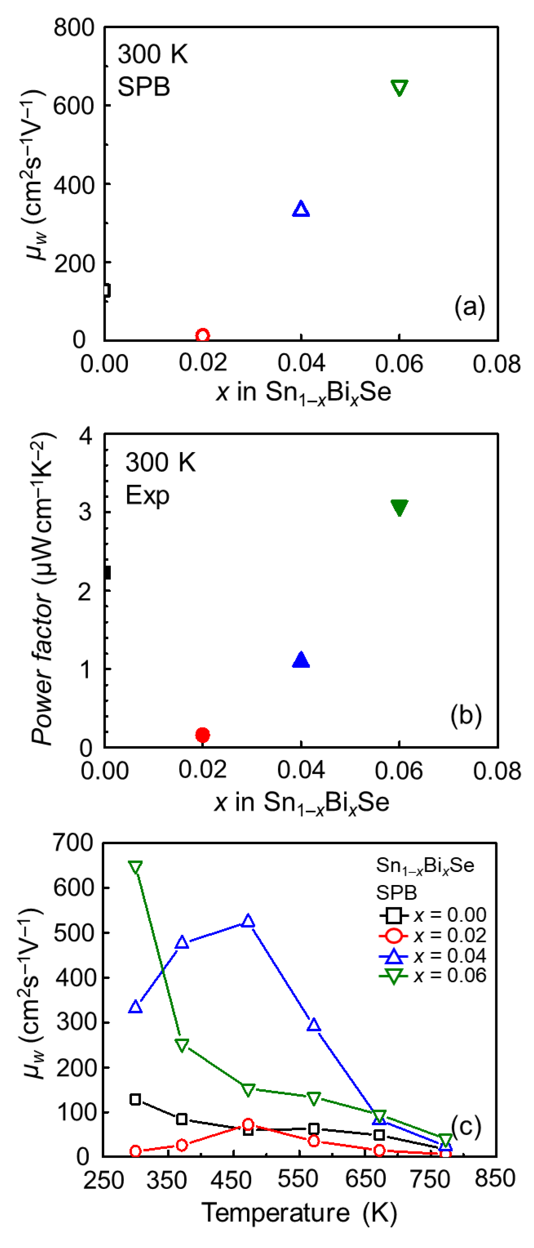
3.3. Calculation of Weighted Mobility, μW

Figure 3 presents μW calculated from experimental σ, S, and T using Equation (6) [23]. Figure 3a shows μW calculated at 300 K.
At 300 K, the calculated μW is highest when x = 0.06 (~650 cm2 s−1 V−1). Physically, the μW is defined as a product between μ0 and (md*/me)3/2, and it is directly proportional to the maximum power factor of a sample. The theoretically maximum power factor can be obtained when the nH of the sample is optimally tuned. Hence, when the band parameter, μW, of different samples are compared, a more promising sample (or composition) can be easily chosen. Therefore, the x = 0.06 sample with the highest μW at 300 K tells us that the x = 0.06 sample will exhibit the highest power factor among other samples once its nH is at its optimum. The experimental power factor of Sn1−xBixSe (x = 0.00, 0.02, 0.04, and 0.06) at 300 K is provided in Figure 3b [18]. The plotted values in Figure 3a,b form similar V-shaped graphs. As the x in Sn1−xBixSe varies from 0 to 0.02, μW and the power factor decrease. Subsequently, as x varies from 0.02 to 0.06, μW and the power factor increase. The trends in μW and power factor can be different from each other. The fact that both trends in μW (Figure 3a) and power factor (Figure 3b) are comparable tells us that the nH of all samples are not far from their optimum nH. Figure 3c shows the variation in μW with temperature, which is also obtained by Equation (6). The μW can also be used to see if there is any band convergence benefitting the electronic transport properties. The μW of the x = 0.02 and 0.04 samples peaks near 473 K. The highest μW of x = 0.06 is estimated to be near 300 K, but the rate of μW drop with temperature also decreases near 473 K. We believe that the electronic transport properties’ improvement in Bi-doped SnSe due to band convergence is the strongest near 473 K. However, experimentally, the power factor of the x = 0.04 sample is the highest near 573 K [18]. However, if the nH at 473 K is optimized, the power factor of the x = 0.04 sample at 473 K will be higher than that at 573 K.

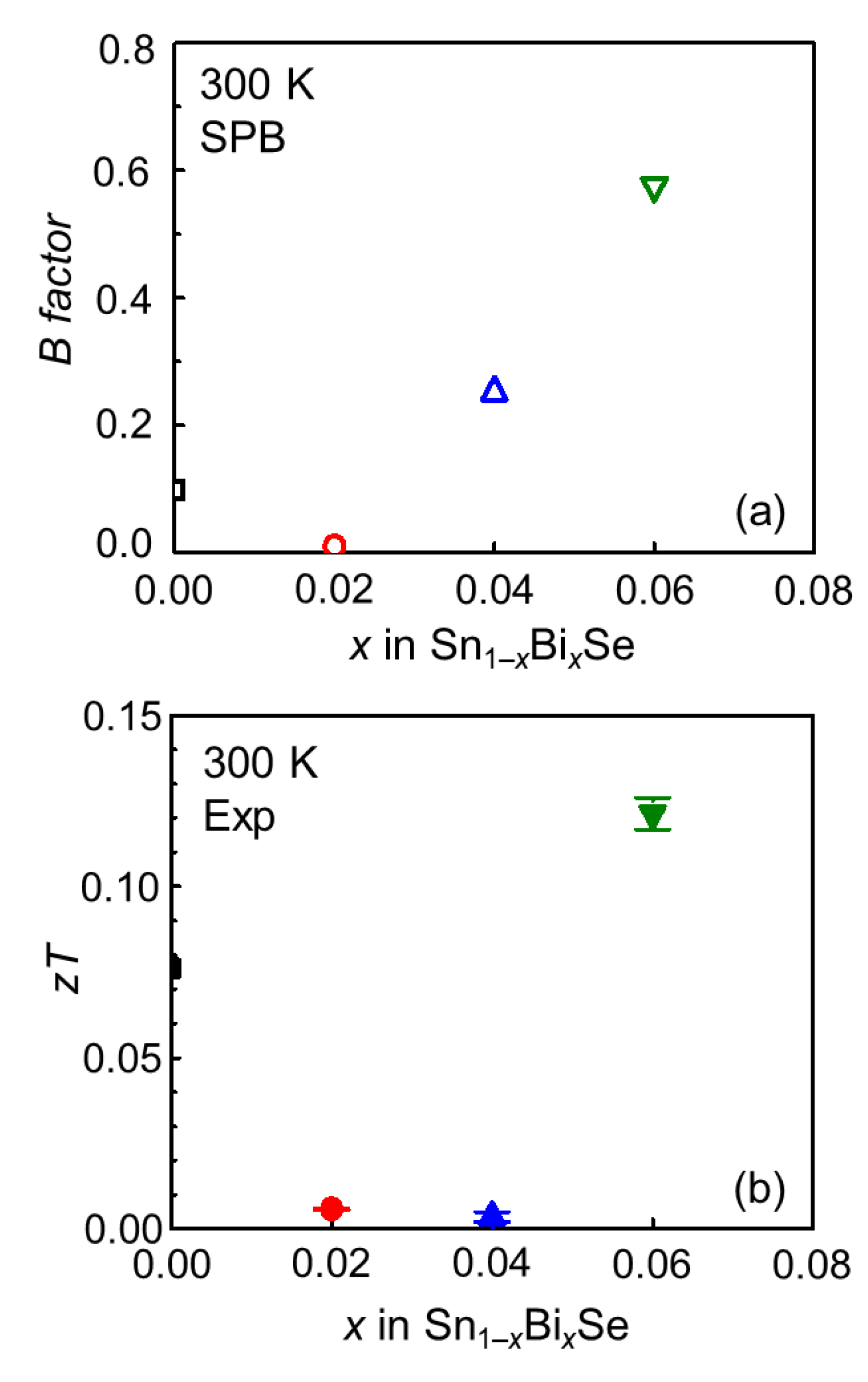
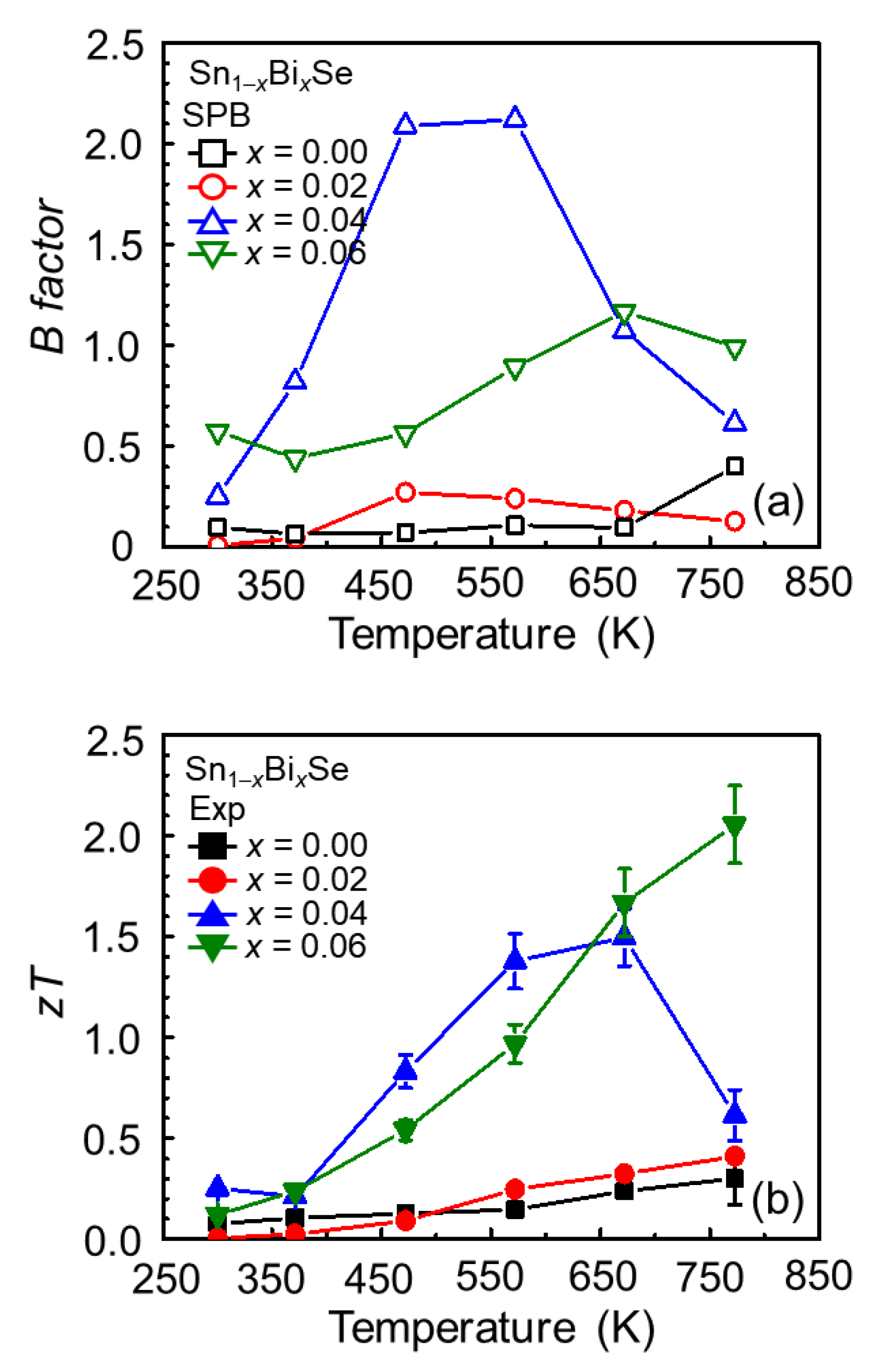
3.4. Calculation of B-Factor

Figure 4 shows the calculated B-factor and the corresponding measured zT at 300 K [18]. The B-factor values shown in Figure 4a are calculated based on the μW in Figure 3 and the experimental κl [18] using Equation (7) [25,26,27,28,29,30]:
The trend observed in the B-factor (Figure 4a) is similar to that observed in μW in Figure 3a. The B-factor first decreases with Bi doping, but with increasing x (Bi doping content), the corresponding B-factor increases. The B-factor when x = 0.02, which is almost 0, improves to ~0.58 when x = 0.06. The fact that the trend in the x-dependent B-factor is similar to that observed in the x-dependent μW tells us that the 300 K κl of the Sn1−xBixSe are also similar to each other. If the discrepancy in κl among the samples with a different x is large, the x-dependent μW must have been changed in the x-dependent B-factor. The 300 K B-factor when x = 0.06 is almost a factor of six greater than that of the undoped SnSe (p-type). Although the μW is directly proportional to the theoretical maximum power factor, the B-factor is not exactly proportional to the theoretical maximum zT. However, the B-factor is related to the theoretical maximum zT. Because the B-factor of the x = 0.06 sample has the highest B-factor, we also expect the highest 300 K zT in the x = 0.06 sample if its nH is not too far from the optimum nH. Figure 4b shows the experimental 300 K zT for different x values, and as predicted in Figure 4a, the zT of the x = 0.06 sample exhibits the highest zT of 0.12 [18]. Experimentally, the 300 K zT of the x = 0.02 and 0.04 are comparable (zT~0.005). However, the 300 K B-factor of the x = 0.04 sample is much higher than that of the x = 0.02 sample. In other words, once the nH is appropriately tuned, the 300 K zT when x = 0.04 can be improved to be much higher than zT of 0.05.
Figure 5 shows the temperature-dependent B-factor and corresponding measured zT. Although, the B-factor when x = 0.04 is lower than that when x = 0.06 at 300 K. For temperatures from 373 to 573 K, the B-factor of the x = 0.04 sample is the highest among other samples. However, the B-factor of the x = 0.06 sample is highest at temperatures higher than 673 K. Initially, the μW of the x = 0.04 sample was the highest for temperatures from 373 to 573 K, with a peak μW at 473 K (Figure 3c). In terms of the B-factor, the peak B-factor is observed at 573 K. This shift of the peak temperature when comparing the temperature μW and B-factor originates from the κl decreasing with temperature. Only the zT of the x = 0.04 sample at 473 and 573 K are the highest, while its B-factor is the highest from 373 to 573 K. Upon nH tuning, the zT of the x = 0.04 sample at 373 K can be much higher than that observed for the x = 0.06 sample at 373 K. Bi doping in SnSe is an effective strategy to improve its mid-temperature zT, as Bi doping can engineer band convergence to maximize its thermoelectric performance.

4. Conclusions

Bi doping transforms SnSe from p-type to n-type, resulting in its high thermoelectric performance. In this study, we calculated four band parameters (density-of-states effective mass (md*), non-degenerate mobility (μ0), weighted mobility (μW), and the B-factor) for Sn1−xBixSe (x = 0.00, 0.02, 0.04, and 0.06) using simple equations and the Single Parabolic Band model. Bi doping can increase both the md* and the μ0 at the same time to improve the electronic transport properties. The physical reason behind the simultaneous improvement in md* and the μ0 with Bi doping can be attributed to suppressed carrier-phonon interaction. Bi doping also changes how the band parameters change with temperature. The two conduction bands in n-type SnSe known to converge near 600 K now converge near 500 K when x = 0.04. The existence of the band convergence is confirmed by the temperature at which the μW peaks. Due to the two conduction bands converging near 500 K in the x = 0.04 sample, the zT of the x = 0.04 sample is highest for temperatures between 473 and 573 K.

Author Contributions

Conceptualization, H.P. and S.-i.K.; validation, S.-i.K.; formal analysis, H.P. and S.-M.H.; writing—original draft preparation, H.P. and S.-i.K.; writing—review and editing, H.-S.K.; visualization, J.-Y.K.; supervision, H.-S.K.; funding acquisition, H.-S.K. All authors have read and agreed to the published version of the manuscript.

Funding

This work was financially supported by the National Research Foundation of Korea (NRF), funded by the Ministry of Education (NRF-2021K2A9A1A06092290).

Data Availability Statement

The data presented in this study are available on request from the corresponding author.

Conflicts of Interest

The authors declare no conflict of interest.

References

  1. Cenci, M.P.; Scarazzato, T.; Munchen, D.D.; Dartora, P.C.; Veit, H.M.; Bernardes, A.M.; Dias, P.R. Eco-Friendly Electronics-A Comprehensive Review. Adv. Mater. Technol. 2021, 7, 2001263. [Google Scholar] [CrossRef]
  2. Lee, J.; Kim, D.H.; Lee, S.T.; Lim, J.K. Fundamental Study of Energy Harvesting Using Thermoelectric Effect on Concrete Structure in Road. Adv. Mater. Res. 2014, 1044–1045, 332–337. [Google Scholar] [CrossRef]
  3. Wei, J.; Yang, L.; Ma, Z.; Song, P.; Zhang, M.; Ma, J.; Yang, F.; Wang, X. Review of current high-ZT thermoelectric materials. J. Mater. Sci. 2020, 55, 12642–12701. [Google Scholar] [CrossRef]
  4. Kutorasinski, K.; Wiendlocha, B.; Kaprzyk, S.; Tobola, J. Electronic structure and thermoelectric properties of n- and p-type SnSe from first principles calculations. Phys. Rev. B 2015, 91, 205201. [Google Scholar] [CrossRef]
  5. Lee, K.H.; Kim, Y.-M.; Park, C.O.; Shin, W.H.; Kim, S.W.; Kim, H.-S.; Kim, S.-I. Cumulative defect structures for experimentally attainable low thermal conductivity in thermoelectric (Bi,Sb)2Te3 alloys. Mater. Today Energy 2021, 21, 100795. [Google Scholar] [CrossRef]
  6. Cai, S.; Hao, S.; Luo, Y.; Su, X.; Luo, Z.-Z.; Hu, X.; Wolverton, C.; Dravid, V.P.; Kanatzidis, M.G. Ultralow Thermal Conductivity and Thermoelectric Properties of Rb2Bi8Se13. Chem. Mater. 2020, 32, 3561–3569. [Google Scholar] [CrossRef]
  7. Pei, Y.; Lensch-Falk, J.; Toberer, E.S.; Medlin, D.L.; Snyder, G.J. High Thermoelectric Performance in PbTe Due to Large Nanoscale Ag2Te Precipitates and La Doping. Adv. Funct. Mater. 2011, 21, 241–249. [Google Scholar] [CrossRef]
  8. Zhang, X.; Zhao, L.-D. Thermoelectric materials: Energy conversion between heat and electricity. J. Mater. 2015, 1, 92–105. [Google Scholar] [CrossRef]
  9. Banik, A.; Shenoy, U.S.; Anand, S.; Waghmare, U.V.; Biswas, K. Mg Alloying in SnTe Facilitates Valence Band Convergence and Optimizes Thermoelectric Properties. Chem. Mater. 2015, 27, 581–587. [Google Scholar] [CrossRef]
  10. Takagiwa, Y.; Pei, Y.; Pomrehn, G.; Snyder, G.J. Dopants effect on the band structure of PbTe thermoelectric material. Appl. Phys. Lett. 2012, 101, 092102. [Google Scholar] [CrossRef] [Green Version]
  11. Ding, G.; Si, J.; Yang, S.; Wang, G.; Wu, H. High thermoelectric properties of n-type Cd-doped PbTe prepared by melt spinning. Scr. Mater. 2016, 122, 1–4. [Google Scholar] [CrossRef]
  12. Zhai, H.; Xiao, Y.; Zhao, L.-D.; Tan, G.; Tang, X. Large effective mass and low lattice thermal conductivity contributing to high thermoelectric performance of Zn-doped Cu5Sn2Se7. J. Alloys Compd. 2020, 826, 154154. [Google Scholar] [CrossRef]
  13. Lee, Y.K.; Luo, Z.; Cho, S.P.; Kanatzidis, M.G.; Chung, I. Surface Oxide Removal for Polycrystalline SnSe Reveals Near-Single-Crystal Thermoelectric Performance. Joule 2019, 3, 719–731. [Google Scholar] [CrossRef]
  14. Sales, B.C.; Mandrus, D.; Williams, R.K. Filled Skutterudite Antimonides: A New Class of Thermoelectric Materials. Science 1996, 272, 1325–1328. [Google Scholar] [CrossRef] [PubMed]
  15. Li, W.; Xu, T.; Ma, Z.; Cheng, Y.; Li, J.; Jiang, Q.; Luo, Y.; Yang, J. High thermoelectric performance in p-type InSb with all-scale hierarchical architectures. Mater. Today Energy 2022, 29, 101091. [Google Scholar] [CrossRef]
  16. Jang, H.; Toriyama, M.Y.; Abbey, S.; Frimpong, B.; Male, J.P.; Snyder, G.J.; Jung, Y.S.; Oh, M.-W. Suppressing Charged Cation Antisites via Se Vapor Annealing Enables p-Type Dopability in AgBiSe2–SnSe Thermoelectrics. Adv. Mater. 2022, 34, 2204132. [Google Scholar] [CrossRef] [PubMed]
  17. Shi, X.-L.; Zou, J.; Chen, Z.-G. Advanced thermoelectric design: From materials and structures to device. Chem. Rev. 2020, 120, 7399–7515. [Google Scholar] [CrossRef] [PubMed]
  18. Duong, A.T.; Nguyen, V.Q.; Duvjir, G.; Duong, V.T.; Kwon, S.; Song, J.Y.; Lee, J.K.; Lee, J.E.; Min, T.; Lee, J.; et al. Achieving ZT = 2.2 with Bi-doped n-type SnSe single crystals. Nat. Commun. 2016, 7, 13713. [Google Scholar] [CrossRef]
  19. Lim, J.-C.; Kim, S.Y.; Shin, W.H.; Kim, S.-I.; Roh, J.W.; Yang, H.; Kim, H.-S. Characterization of Hall factor with Seebeck coefficient measurement. ACS Appl. Energy Mater. 2022, 5, 4036. [Google Scholar] [CrossRef]
  20. Lee, K.H.; Kim, S.-I.; Lim, J.-C.; Cho, J.Y.; Yang, H.; Kim, H.-S. Approach to Determine the Density-of-States Effective Mass with Carrier Concentration-Dependent Seebeck Coefficient. Adv. Funct. Mater. 2022, 32, 2203852. [Google Scholar] [CrossRef]
  21. May, A.F.; Snyder, G.J. Introduction to modeling thermoelectric transport at high temperatures. In Thermoelectrics and Its Energy Harvesting; Rowe, D.M., Ed.; CRC Press: London, UK, 2012; Volume 1, pp. 1–18. [Google Scholar]
  22. Kim, M.; Kim, S.-I.; Kim, S.W.; Kim, H.-S.; Lee, K.H. Weighted Mobility Ratio Engineering for High-Performance Bi–Te-Based Thermoelectric Materials via Suppression of Minority Carrier Transport. Adv. Mater. 2021, 33, 2005931. [Google Scholar] [CrossRef] [PubMed]
  23. Snyder, G.J.; Snyder, A.H.; Wood, M.; Gurunathan, R.; Snyder, B.H.; Niu, C. Weighted Mobility. Adv. Mater. 2020, 32, 2001537. [Google Scholar] [CrossRef] [PubMed]
  24. Chang, C.; Wu, M.; He, D.; Pei, Y.; Wu, C.-F.; We, X.; Yu, H.; Zhu, F.; Wang, K.; Chen, Y.; et al. 3D charge and 2D phonon transports leading to high out-of-plane ZT in n-type SnSe crystals. Science 2018, 360, 778. [Google Scholar] [CrossRef]
  25. Witting, I.T.; Chasapis, T.C.; Ricci, F.; Peters, M.; Heinz, N.A.; Hautier, G.; Snyder, G.J. The Thermoelectric Properties of Bismuth Telluride. Adv. Electron. Mater. 2019, 5, 1800904. [Google Scholar] [CrossRef]
  26. Wang, H.; Pei, Y.; LaLonde, A.D.; Snyder, G.J. Material design considerations based on thermoelectric quality factor. In Thermoelectric Nanomaterials; Kumoto, K., Mori, T., Eds.; Springer: Berlin, Germany, 2013; pp. 1–32. [Google Scholar]
  27. Pei, Y.; Wang, H.; Snyder, G.J. Band Engineering of Thermoelectric Materials. Adv. Mater. 2021, 4, 6125. [Google Scholar] [CrossRef] [PubMed]
  28. Pei, Y.; LaLonde, A.D.; Wang, H.; Snyder, G.J. Low effective mass leading to high thermoelectric performance. Energy Environ. Sci. 2012, 5, 7963. [Google Scholar] [CrossRef]
  29. Zhang, X.; Bu, Z.; Shi, X.; Chen, Z.; Kin, S.; Shan, B.; Wood, M.; Snyder, A.H.; Chen, L.; Snyder, G.J.; et al. Electronic quality factor for thermoelectrics. Sci. Adv. 2020, 6, eabc0726. [Google Scholar] [CrossRef]
  30. Devlin, K.P.; Chen, S.; Donadio, D.; Kauzlarich, S.M. Solid Solution Yb2–xCaxCdSb2: Structure, Thermoelectric Properties, and Quality Factor. Inorg. Chem. 2021, 60, 13596. [Google Scholar] [CrossRef]
Figure 1. (a) Calculated (lines) and experimental (symbols) magnitude of Seebeck coefficient (|S|)-dependent log10(n) for Sn1−xBixSe (x = 0.00, 0.02, 0.04, and 0.06) at 300 K [18], (b) calculated density-of-states effective mass (md*) varying with x in Sn1−xBixSe (x = 0.00, 0.02, 0.04, and 0.06) at 300 K, and (c) calculated md* for Sn1−xBixSe (x = 0.00, 0.02, 0.04, and 0.06) varying with temperature (300–773 K).
Ceramics 06 00029 g001
Figure 2. (a) Calculated (lines) and experimental (symbols) nH-dependent Hall mobility (μH) for Sn1−xBixSe (x = 0.00, 0.02, 0.04, and 0.06) at 300 K [18], (b) calculated non-degenerate mobility (μ0) varying with x in Sn1−xBixSe (x = 0.00, 0.02, 0.04, and 0.06) at 300 K, and (c) calculated μ0 for Sn1−xBixSe (x = 0.00, 0.02, 0.04, and 0.06) varying with temperature (300–773 K).
Ceramics 06 00029 g002
Figure 3. (a) Calculated weighted mobility (μW) varying with x in Sn1−xBixSe (x = 0.00, 0.02, 0.04, and 0.06) at 300 K, (b) experimental power factor varying with x in Sn1−xBixSe (x = 0.00, 0.02, 0.04, and 0.06) at 300 K [18], and (c) calculated μW for Sn1−xBixSe (x = 0.00, 0.02, 0.04, and 0.06) varying with temperature (300–773 K).
Ceramics 06 00029 g003
Figure 4. (a) Calculated B-factor varying with x in Sn1−xBixSe (x = 0.00, 0.02, 0.04, and 0.06) at 300 K, (b) experimental zT varying with x in Sn1−xBixSe (x = 0.00, 0.02, 0.04, and 0.06) at 300 K [18].
Ceramics 06 00029 g004
Figure 5. (a) Calculated temperature-dependent B-factor varying with x in Sn1−xBixSe (x = 0.00, 0.02, 0.04, and 0.06), (b) experimental temperature-dependent zT varying with x in Sn1−xBixSe (x = 0.00, 0.02, 0.04, and 0.06) [18].
Ceramics 06 00029 g005
Disclaimer/Publisher’s Note: The statements, opinions and data contained in all publications are solely those of the individual author(s) and contributor(s) and not of MDPI and/or the editor(s). MDPI and/or the editor(s) disclaim responsibility for any injury to people or property resulting from any ideas, methods, instructions or products referred to in the content.

