
Electrostatically Driven Vertical Combinatorial Patterning of Colloidal Nano-Objects

 , and
, and 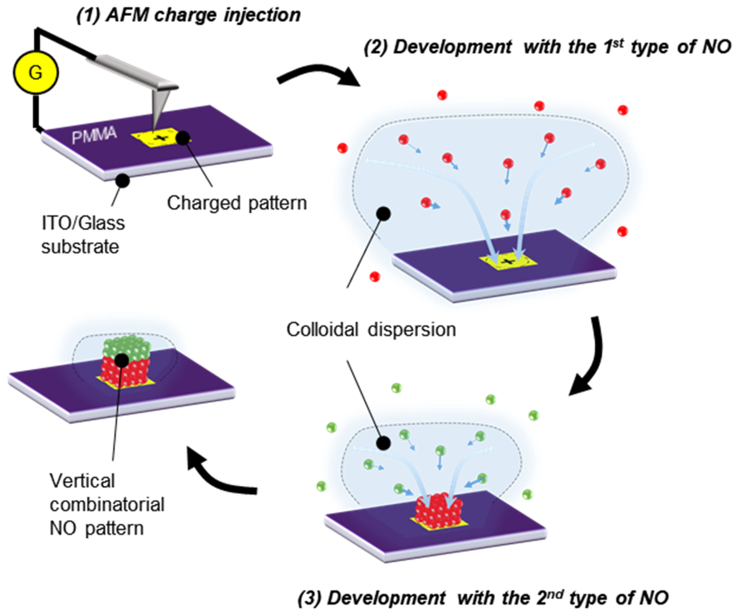
Abstract
:1. Introduction
2. Materials and Methods
2.1. Vertical Combinatorial Patterning by AFM Nanoxerography
2.2. Topographical and Optical Characterizations of NP Co-Assemblies
2.3. Simulations of the Optical Emission of the Vertical Combinatorial NP Patterns
3. Results
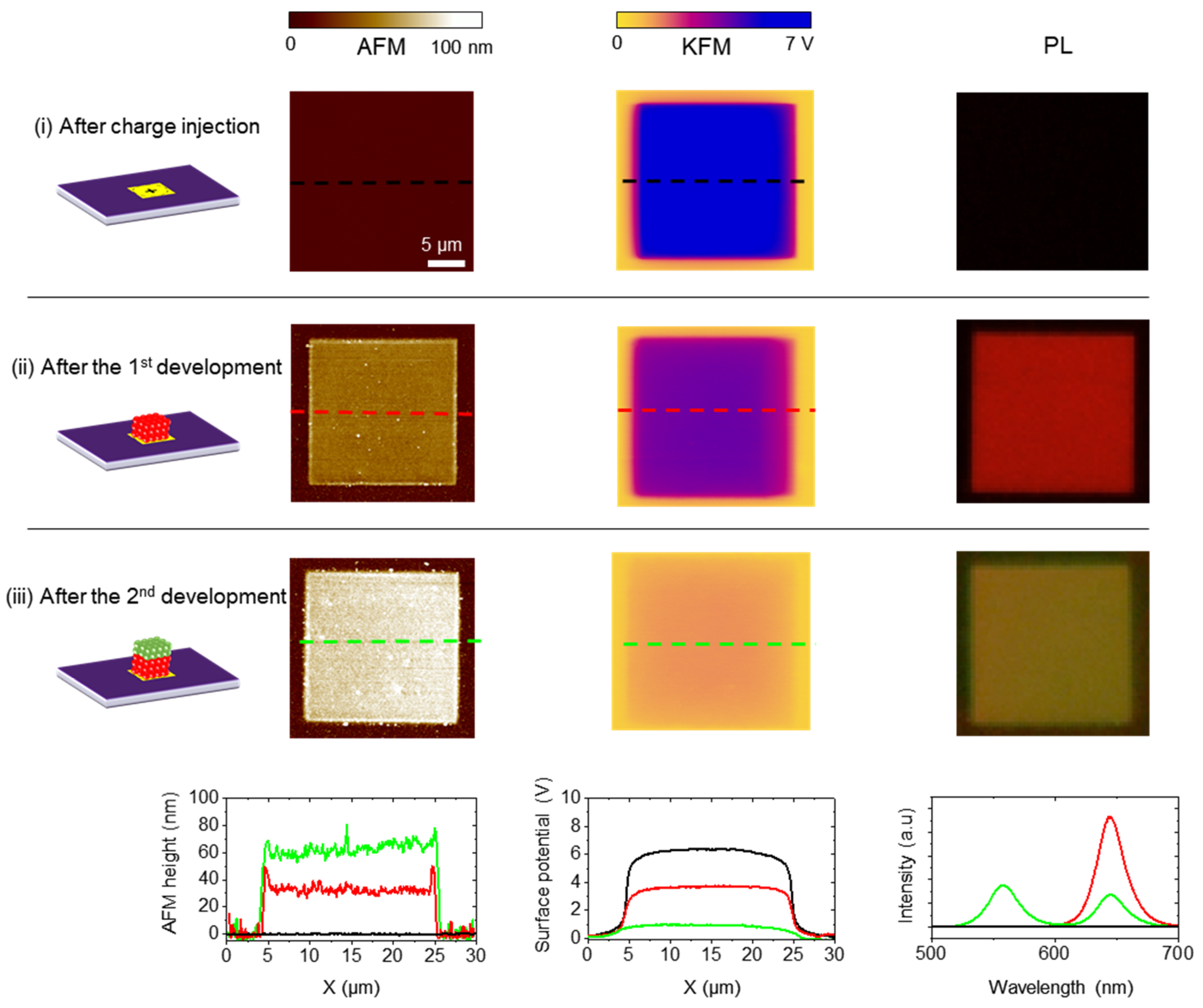
3.1. Proof of Concept of NP Vertical Co-Assembly
3.2. Applications for Dual Colored Patterns
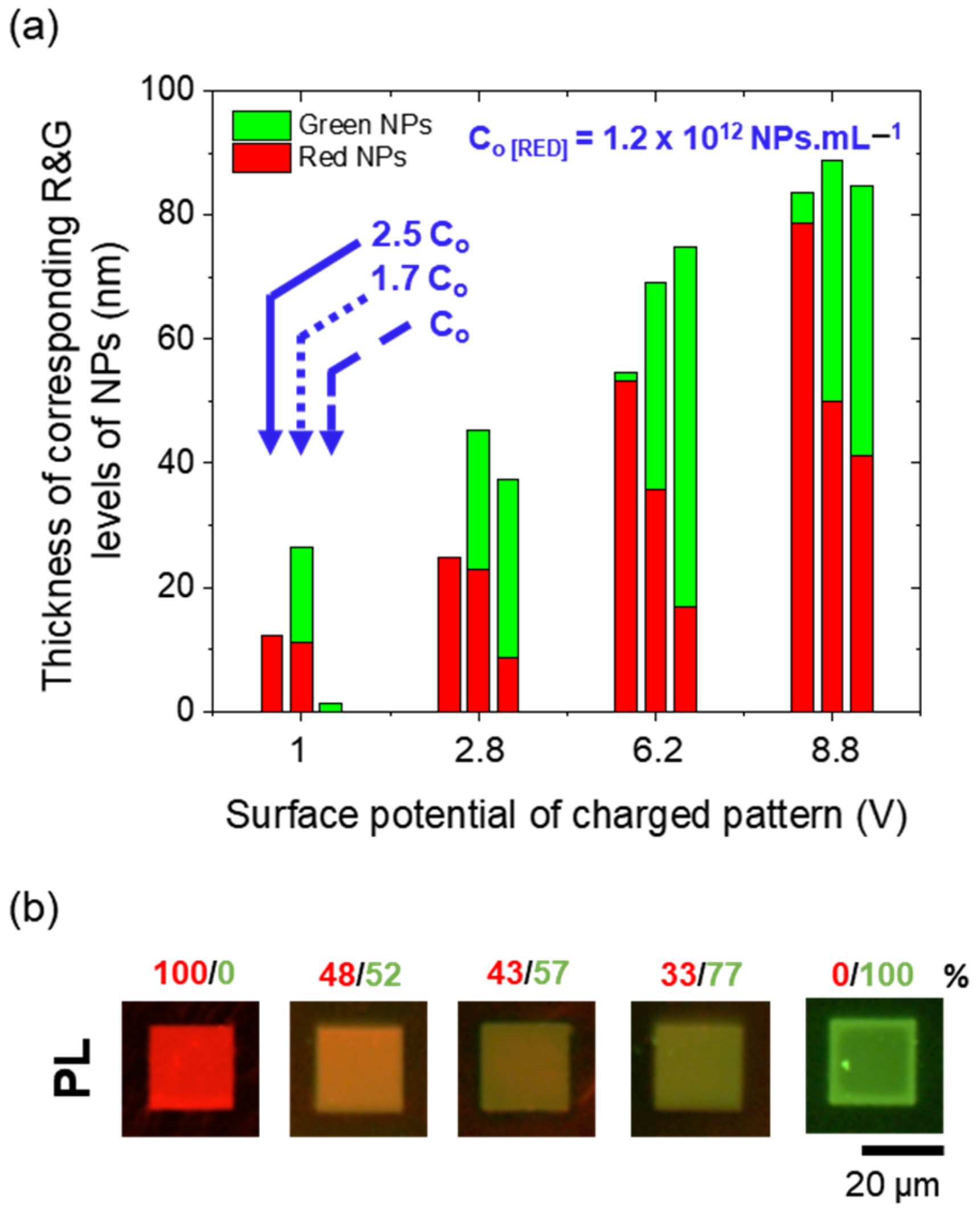
3.2.1. Tuning the Thickness of Each NP Level
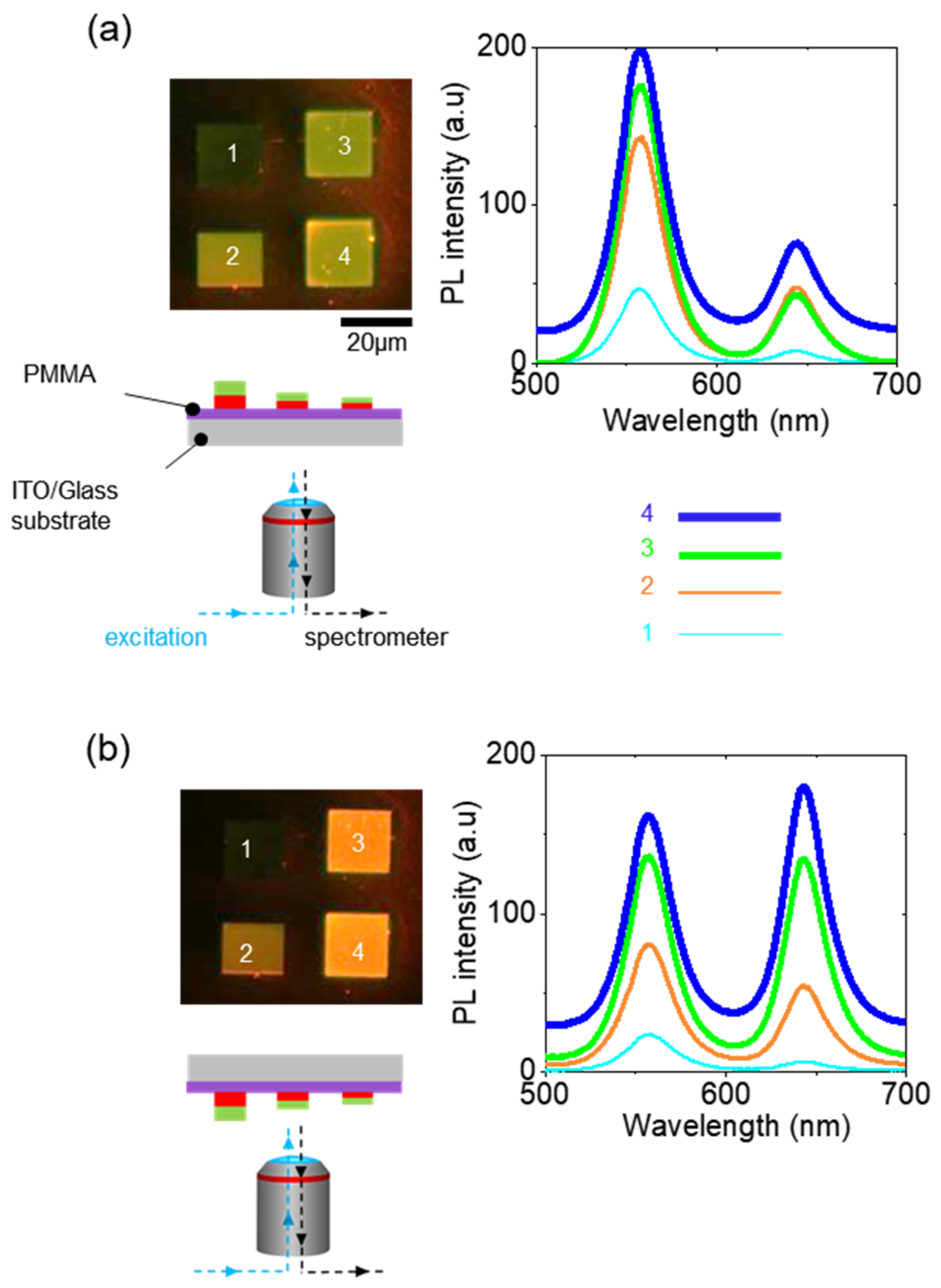
3.2.2. Flipping the Sample
4. Discussion
5. Conclusions
Author Contributions
Funding
Data Availability Statement
Conflicts of Interest
References
- Grzelczak, M.; Vermant, J.; Furst, E.M.; Liz-Marzán, L.M. Directed Self-Assembly of Nanoparticles. ACS Nano 2010, 4, 3591–3605. [Google Scholar] [CrossRef] [PubMed]
- Kumar, P. Directed Self-Assembly: Expectations and Achievements. Nanoscale Res. Lett. 2010, 5, 1367–1376. [Google Scholar] [CrossRef] [PubMed] [Green Version]
- Vogel, N.; Retsch, M.; Fustin, C.-A.; del Campo, A.; Jonas, U. Advances in Colloidal Assembly: The Design of Structure and Hierarchy in Two and Three Dimensions. Chem. Rev. 2015, 115, 6265–6311. [Google Scholar] [CrossRef]
- von Bojnicic-Kninski, C.; Popov, R.; Dörsam, E.; Loeffler, F.F.; Breitling, F.; Nesterov-Mueller, A. Combinatorial Particle Patterning. Adv. Funct. Mater. 2017, 27, 1703511. [Google Scholar] [CrossRef]
- Choi, M.K.; Yang, J.; Kang, K.; Kim, D.C.; Choi, C.; Park, C.; Kim, S.J.; Chae, S.I.; Kim, T.-H.; Kim, J.H.; et al. Wearable Red-Green-Blue Quantum Dot Light-Emitting Diode Array Using High-Resolution Intaglio Transfer Printing. Nat. Commun. 2015, 6. [Google Scholar] [CrossRef] [Green Version]
- Dai, X.; Deng, Y.; Peng, X.; Jin, Y. Quantum-Dot Light-Emitting Diodes for Large-Area Displays: Towards the Dawn of Commercialization. Adv. Mater. 2017, 29, 1607022. [Google Scholar] [CrossRef]
- Kim, T.-H.; Cho, K.-S.; Lee, E.K.; Lee, S.J.; Chae, J.; Kim, J.W.; Kim, D.H.; Kwon, J.-Y.; Amaratunga, G.; Lee, S.Y.; et al. Full-Colour Quantum Dot Displays Fabricated by Transfer Printing. Nat. Photonics 2011, 5, 176–182. [Google Scholar] [CrossRef]
- Yang, S.M.; Jang, S.G.; Choi, D.G.; Kim, S.; Yu, H.K. Nanomachining by Colloidal Lithography. Small 2006, 2, 458–475. [Google Scholar] [CrossRef]
- Stadler, V.; Felgenhauer, T.; Beyer, M.; Fernandez, S.; Leibe, K.; Güttler, S.; Gröning, M.; König, K.; Torralba, G.; Hausmann, M.; et al. Combinatorial Synthesis of Peptide Arrays with a Laser Printer. Angew. Chem. Int. Ed. 2008, 47, 7132–7135. [Google Scholar] [CrossRef]
- Zeng, A.-P. (Ed.) Fundamentals and Application of New Bioproduction Systems; Advances in Biochemical Engineering/Biotechnology; Springer: Berlin/Heidelberg, Germany, 2013; Volume 137, ISBN 978-3-642-41520-3. [Google Scholar]
- Carlson, A.; Bowen, A.M.; Huang, Y.; Nuzzo, R.G.; Rogers, J.A. Transfer Printing Techniques for Materials Assembly and Micro/Nanodevice Fabrication. Advanced Materials 24 2012, 24, 5284–5318. [Google Scholar] [CrossRef]
- Nayak, L.; Mohanty, S.; Nayak, S.K.; Ramadoss, A. A Review on Inkjet Printing of Nanoparticle Inks for Flexible Electronics. J. Mater. Chem. C 2019, 7, 8771–8795. [Google Scholar] [CrossRef]
- Ni, S.; Isa, L.; Wolf, H. Capillary Assembly as a Tool for the Heterogeneous Integration of Micro- and Nanoscale Objects. Soft Matter 2018, 14, 2978–2995. [Google Scholar] [CrossRef] [PubMed]
- Erb, R.M.; Son, H.S.; Samanta, B.; Rotello, V.M.; Yellen, B.B. Magnetic Assembly of Colloidal Superstructures with Multipole Symmetry. Nature 2009, 457, 999–1002. [Google Scholar] [CrossRef] [PubMed]
- Yang, P.; Li, C.L.; Murase, N. Highly Photoluminescent Multilayer QD−Glass Films Prepared by LbL Self-Assembly. Langmuir 2005, 21, 8913–8917. [Google Scholar] [CrossRef] [PubMed]
- Hua, F.; Shi, J.; Lvov, Y.; Cui, T. Patterning of Layer-by-Layer Self-Assembled Multiple Types of Nanoparticle Thin Films by Lithographic Technique. Nano Lett. 2002, 2, 1219–1222. [Google Scholar] [CrossRef]
- Cui, T.; Hua, F.; Lvov, Y. Lithographic Approach to Pattern Multiple Nanoparticle Thin Films Prepared by Layer-by-Layer Self-Assembly for Microsystems. Sens. Actuators A Phys. 2004, 114, 501–504. [Google Scholar] [CrossRef]
- Gao, M.; Sun, J.; Dulkeith, E.; Gaponik, N.; Lemmer, U.; Feldmann, J. Lateral Patterning of CdTe Nanocrystal Films by the Electric Field Directed Layer-by-Layer Assembly Method. Langmuir 2002, 18, 4098–4102. [Google Scholar] [CrossRef]
- Wang, Y.; Liu, Y.; Cheng, Y.; Kim, E.; Rubloff, G.W.; Bentley, W.E.; Payne, G.F. Coupling Electrodeposition with Layer-by-Layer Assembly to Address Proteins within Microfluidic Channels. Adv. Mater. 2011, 23, 5817–5821. [Google Scholar] [CrossRef]
- Jacobs, H.O.; Campbell, S.A.; Steward, M.G. Approaching Nanoxerography: The Use of Electrostatic Forces to Position Nanoparticles with 100 Nm Scale Resolution. Adv. Mater. 2002, 14, 1553–1557. [Google Scholar] [CrossRef]
- Palleau, E.; Ressier, L. Combinatorial Particle Patterning by Nanoxerography. Adv. Funct. Mater. 2018, 28, 1801075. [Google Scholar] [CrossRef]
- Xing, X.; Man, Z.; Bian, J.; Yin, Y.; Zhang, W.; Lu, Z. High-Resolution Combinatorial Patterning of Functional Nanoparticles. Nat. Commun. 2020, 11, 6002. [Google Scholar] [CrossRef]
- Palleau, E.; Sangeetha, N.M.; Viau, G.; Marty, J.-D.; Ressier, L. Coulomb Force Directed Single and Binary Assembly of Nanoparticles from Aqueous Dispersions by AFM Nanoxerography. ACS Nano 2011, 5, 4228–4235. [Google Scholar] [CrossRef]
- Midelet, C.; Petit, G.; Raffy, S.; Hallez, Y.; Mendes-Marinho, S.; Pousthomis, M.; D’Amico, M.; Guérin, F.; Palleau, E.; Ressier, L. On the in Situ 3D Electrostatic Directed Assembly of CdSe/CdZnS Colloidal Quantum Nanoplatelets towards Display Applications. J. Colloid Interface Sci. 2022, 630, 924–933. [Google Scholar] [CrossRef]
- Qu, J.; Rastogi, P.; Gréboval, C.; Livache, C.; Dufour, M.; Chu, A.; Chee, S.-S.; Ramade, J.; Xu, X.Z.; Ithurria, S.; et al. Nanoplatelet-Based Light-Emitting Diode and Its Use in All-Nanocrystal LiFi-like Communication. ACS Appl. Mater. Interfaces 2020, 12, 22058–22065. [Google Scholar] [CrossRef]
- Tessier, M.D.; Mahler, B.; Nadal, B.; Heuclin, H.; Pedetti, S.; Dubertret, B. Spectroscopy of Colloidal Semiconductor Core/Shell Nanoplatelets with High Quantum Yield. Nano Lett. 2013, 13, 3321–3328. [Google Scholar] [CrossRef] [PubMed]
- Ressier, L.; Le Nader, V. Electrostatic Nanopatterning of PMMA by AFM Charge Writing for Directed Nano-Assembly. Nanotechnology 2008, 19, 135301. [Google Scholar] [CrossRef] [PubMed]
- Wiecha, P.R. PyGDM—A Python Toolkit for Full-Field Electro-Dynamical Simulations and Evolutionary Optimization of Nanostructures. Comput. Phys. Commun. 2018, 233, 167–192. [Google Scholar] [CrossRef] [Green Version]
- Wiecha, P.R.; Cuche, A.; Arbouet, A.; Girard, C.; Colas des Francs, G.; Lecestre, A.; Larrieu, G.; Fournel, F.; Larrey, V.; Baron, T.; et al. Strongly Directional Scattering from Dielectric Nanowires. ACS Photonics 2017, 4, 2036–2046. [Google Scholar] [CrossRef] [Green Version]
- Lisitsa, M.P.; Gudymenko, L.F.; Malinko, V.N.; Terekhova, S.F. Dispersion of the Refractive Indices and Birefringence of CdSxSe1−x Single Crystals. Phys. Status Solidi 1969, 31, 389–399. [Google Scholar] [CrossRef]
- Lyuksyutov, S.F.; Vaia, R.A.; Paramonov, P.B.; Juhl, S.; Waterhouse, L.; Ralich, R.M.; Sigalov, G.; Sancaktar, E. Electrostatic Nanolithography in Polymers Using Atomic Force Microscopy. Nat. Mater. 2003, 2, 468–472. [Google Scholar] [CrossRef]
- Jones, T.B. Electromechanics of Particles; Cambridge University Press: Cambridge, UK, 1995. [Google Scholar]
- Palleau, E.; Sangeetha, N.M.; Ressier, L. Quantification of the Electrostatic Forces Involved in the Directed Assembly of Colloidal Nanoparticles by AFM Nanoxerography. Nanotechnology 2011, 22, 325603. [Google Scholar] [CrossRef]
- Platel, R.; Vaure, L.; Palleau, E.; Raffy, S.; Guérin, F.; Lagarde, D.; Cours, R.; Marcelot, C.; Warot-Fonrose, B.; Nayral, C.; et al. Synthesis of Hybrid Colloidal Nanoparticles for a Generic Approach to 3D Electrostatic Directed Assembly: Application to Anti-Counterfeiting. J. Colloid Interface Sci. 2021, 582, 1243–1250. [Google Scholar] [CrossRef] [PubMed]
- Moutet, P.; Deram, P.; Sangeetha, N.M.; Ressier, L. Dynamics of Dielectrophoretic-Force-Directed Assembly of NaYF4 Colloidal Nanocrystals into Tunable Multilayered Micropatterns. J. Phys. Chem. Lett. 2014, 5, 2988–2993. [Google Scholar] [CrossRef]
- Jacobs, H.O.; Whitesides, G.M. Submicrometer Patterning of Charge in Thin-Film Electrets. Science 2001, 291, 1763–1766. [Google Scholar] [CrossRef] [PubMed] [Green Version]
- Poirot, D.; Platel, R.; Alnasser, T.; Guerin, F.; Palleau, E.; Ressier, L. Smartphone-Identifiable Photoluminescent Nanoparticle-Based Multilevel Secured Tags by Electrical Microcontact Printing. ACS Appl. Nano Mater. 2018, 1, 5936–5943. [Google Scholar] [CrossRef]
- Ressier, L.; Palleau, E.; Behar, S. Electrical Nano-Imprint Lithography. Nanotechnology 2012, 23, 255302. [Google Scholar] [CrossRef] [PubMed]


Disclaimer/Publisher’s Note: The statements, opinions and data contained in all publications are solely those of the individual author(s) and contributor(s) and not of MDPI and/or the editor(s). MDPI and/or the editor(s) disclaim responsibility for any injury to people or property resulting from any ideas, methods, instructions or products referred to in the content. |
© 2023 by the authors. Licensee MDPI, Basel, Switzerland. This article is an open access article distributed under the terms and conditions of the Creative Commons Attribution (CC BY) license (https://creativecommons.org/licenses/by/4.0/).
Share and Cite
Petit, G.; Hernandez, R.; Raffy, S.; Cuche, A.; Soria Marina, L.; D’Amico, M.; Palleau, E.; Ressier, L. Electrostatically Driven Vertical Combinatorial Patterning of Colloidal Nano-Objects. Colloids Interfaces 2023, 7, 6. https://doi.org/10.3390/colloids7010006
Petit G, Hernandez R, Raffy S, Cuche A, Soria Marina L, D’Amico M, Palleau E, Ressier L. Electrostatically Driven Vertical Combinatorial Patterning of Colloidal Nano-Objects. Colloids and Interfaces. 2023; 7(1):6. https://doi.org/10.3390/colloids7010006
Chicago/Turabian StylePetit, Gaëtan, Romain Hernandez, Simon Raffy, Aurélien Cuche, Lorena Soria Marina, Michele D’Amico, Etienne Palleau, and Laurence Ressier. 2023. "Electrostatically Driven Vertical Combinatorial Patterning of Colloidal Nano-Objects" Colloids and Interfaces 7, no. 1: 6. https://doi.org/10.3390/colloids7010006