Article

Rapid Prototyping of 3D Printed, High Aspect Ratio, Low Noise Amplifier for Active Handheld Sensor Devices

1
Laboratory for Physical Sciences, College Park, MD 20740, USA
2
Mechanical Engineering Department, University of Maryland, College Park, MD 20742, USA
3
Electrical and Computer Engineering Department, University of Maryland, College Park, MD 20742, USA
*
Author to whom correspondence should be addressed.
Current address: Department of Aeronautics & Astronautics Manufacturing Engineering, Northwestern Polytechnical University, Xi’an 710072, China.
J. Manuf. Mater. Process. 2023, 7(3), 83; https://doi.org/10.3390/jmmp7030083
Submission received: 13 March 2023 / Revised: 21 April 2023 / Accepted: 23 April 2023 / Published: 26 April 2023

Abstract

:
In this paper, we report the use of additive manufacturing methods to fabricate a high aspect ratio, low noise amplifier (LNA) for a handheld active sensor device operating at up to 1 GHz. The new form factor LNA incorporates a modification of a square-shaped commercial off-the-shelf (COTS) LNA into a 5:1 aspect ratio device without a loss in RF performance. For rapid prototyping, we employ both subtractive and additive manufacturing technologies, such as milling, extrusion-based syringe printing, and aerosol jet printing techniques to fabricate both small form factor and high aspect ratio devices. The 5:1 aspect ratio LNA demonstrated a 20% smaller form factor, a gain of 25 dB, and an NF less than 3 dB over an operating frequency range up to 1 GHz, comparable to the COTS LNA. Design, simulation, and experimental results are given to highlight the advantages of 3D printed hybrid electronic technology over the conventional PCB fabrication method for rapid prototyping of RF electronic devices.

1. Introduction

Rapid prototyping has become a crucial engineering technology for creating and improving parts directly from a design concept [1,2,3]. Over the past few decades, rapid prototyping, as it applies to 3D manufacturing technologies, has been demonstrated to reduce design/production times and cost tremendously, at least for small volume production, and has become an integral aspect of 3D additive manufacturing [4,5,6]. The conventional method for the fabrication of circuitization is limited to 2D planar structures, while 3D manufacturing technologies include more flexible capability in terms of design and materials [7,8,9]. There has been a growing interest in the use of 3D printing technology for the fabrication of printed electronics. Various studies have explored the use of 3D printing for the creation of conductive traces, capacitors, and RF electronic components, such as transmission lines and antennas. There are several different 3D printing methods, each with their unique strengths and weaknesses, such as fused deposition modeling (FDM), stereolithography (SLA), inkjet, aerosol jet printing (AJP), selective laser sintering (SLS), direct energy deposition (DED), and electrohydrodynamic (EHD) printing. Previous works on RF devices using various 3D printing technologies are given in Table 1.
Handheld devices encompass a broad range of portable electronic devices that have numerous practical applications in our daily lives, such as smart phones, tablets, and GPS location sensors. Electronic circuits can be printed utilizing various materials to fulfill the specific requirements of applications, such as probes and sensors, even without the use of conventional PCB manufacturing equipment. With advancements in technology, handheld electronic sensors/probes can now be easily and affordably created using 3D printing, which has the potential to greatly improve the way we measure and monitor. A commercial off-the-shelf (COTS) handheld probing device, such as a thermal or electro-magnetic (EM) near-field sensor, has been widely used for debugging, fault detection, electromagnetic interference (EMI)/electromagnetic compatibility (EMC), and compliance testing of RF devices [18,19]. Among these sensors, handheld devices are mostly passive or connected to an external desktop amplifier module via a coaxial cable. Because the signal from such sensors used for near-field detection is typically extremely small, a low noise amplifier (LNA) for preamplification is commonly used as a receiver to boost the signal of interest above the noise floor [20,21]. RF amplification can be achieved simply by using a single transistor, multi-stage monolithic amplifier [22,23]. However, the rapid prototyping of an LNA requiring a low noise figure (NF) and a high gain using additive and subtractive manufacturing method has yet to be explored.
In this paper, we report design and fabrication methods for rapid prototyping of a high aspect ratio LNA that can be used as a compact, active, handheld sensor device. Based on the 2.54 cm (1 in) square COTS LNA (ZFL-1000LN+) from Mini-Circuits® [24] as a reference, we redesigned and fabricated 1:1, 3:1, and 5:1 aspect ratio LNAs with careful consideration of printing parameters and circuit performance. We discuss the 5:1 aspect ratio LNA showing a 20% smaller form factor, a gain of 25 dB, and an NF less than 3 dB over an operating frequency range up to 1 GHz, comparable to the COTS LNA.

2. Design and Methods

Figure 1a shows an example of a 0.5 mm (20 mil) thick triangle-shaped (Rogers® RO4350B substrate) active probing sensor device connected to a COTS LNA. Various sensing elements could be substituted in the probing section, as needed. The size and geometry of this 1:1 ratio LNA inhibits the customization of a device for a handheld active sensor—particularly for a cascade structure, such as the integration of multiple sensors with single or multiple LNAs. Figure 1b illustrates an alternative form factor for such an LNA-based active sensor design that has an aspect ratio of 5:1, where the aspect ratio is defined by the ratio of length to width of a substrate. The probe and the LNA are integrated into a single substrate without the need for additional assembly of an SMA M-M adaptor to connect the sensor to the amplifier (as shown in Figure 1a). Figure 1c shows a proposed LNA without a probe, where length (L) and width (W) can vary for different aspect ratios. Special care was taken in the design for the proposed LNA device to obtain comparable performance to the COTS LNA. We will discuss circuit design, low loss microstrip line, and fabrication in the following paragraphs.

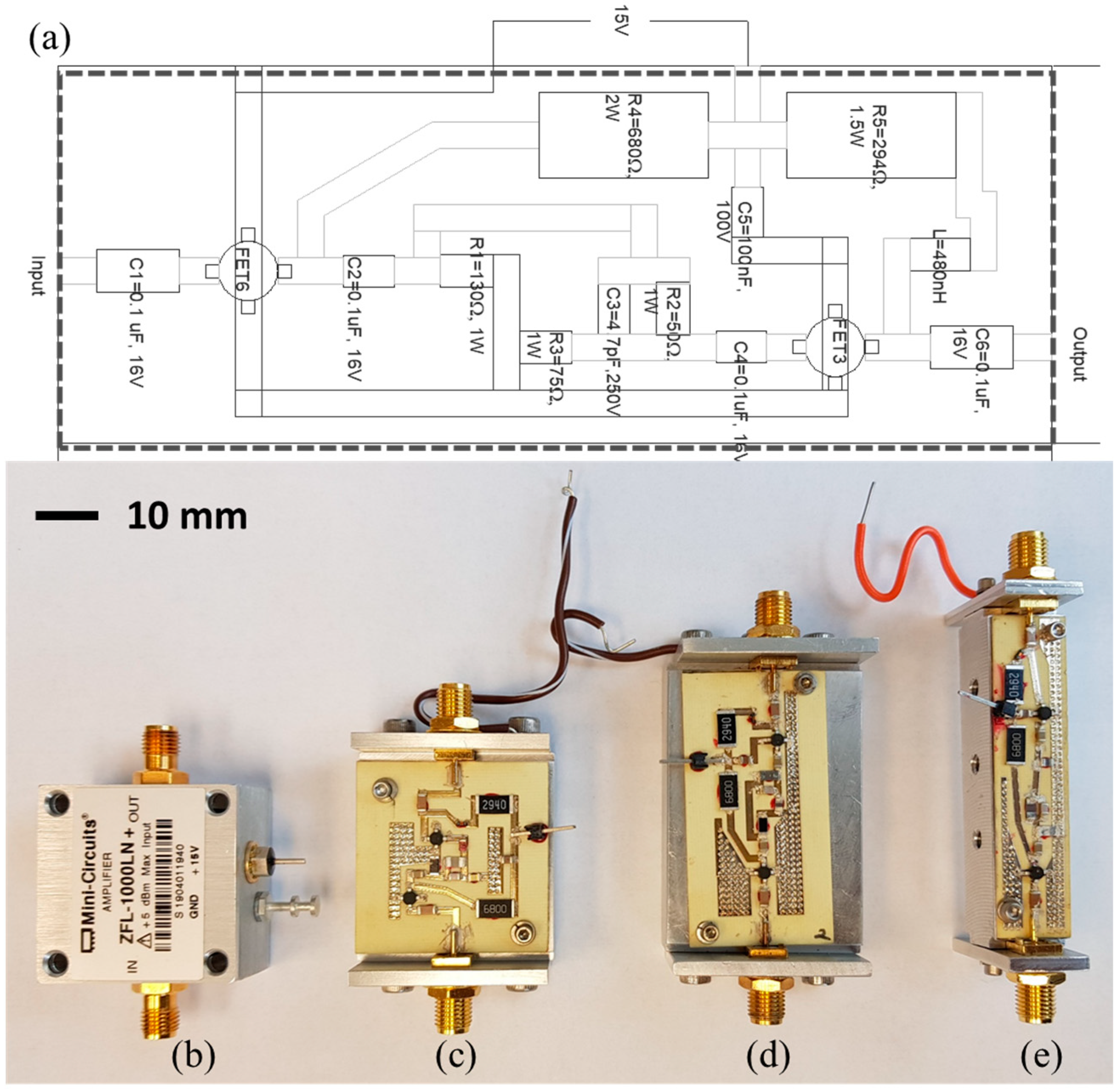
2.1. Circuit Simulation of Redistributed Circuit Layout

The reference COTS LNA is a wide band LNA operating from 0.1 MHz to 1 GHz [24]. It has an NF of 3 dB and a gain of 23 dB with a feed voltage of VDC = 15 V. Using the Keysight® Advanced Design System (ADS) circuit simulator software, the circuit components were rearranged to model 1:1, 3:1, and 5:1 aspect ratio LNAs. The modified circuit layouts were then converted to distributed circuit models in order to simulate gain and NF. This was carried out using the PC board (PCB) layout tool in the ADS simulator. Figure 2a shows an example of the AUTOCAD® schematic for the 3:1 circuit design and fabrication, and Figure 2b–e show the COTS LNA (1:1) and the fabricated LNAs with aspect ratios of 1:1, 3:1, and 5:1, respectively. Simulations of these three versions (c–e) showed that a 5 cm (2 in) long LNA for a 5:1 aspect ratio was the largest possible aspect ratio that would result in RF loss comparable with the other two aspect ratio LNAs because of the dependence on the size of the transmission lines, line-to-line spacing, field effect transistors (FET), resistor, capacitor, and inductor surface mount devices (SMDs).

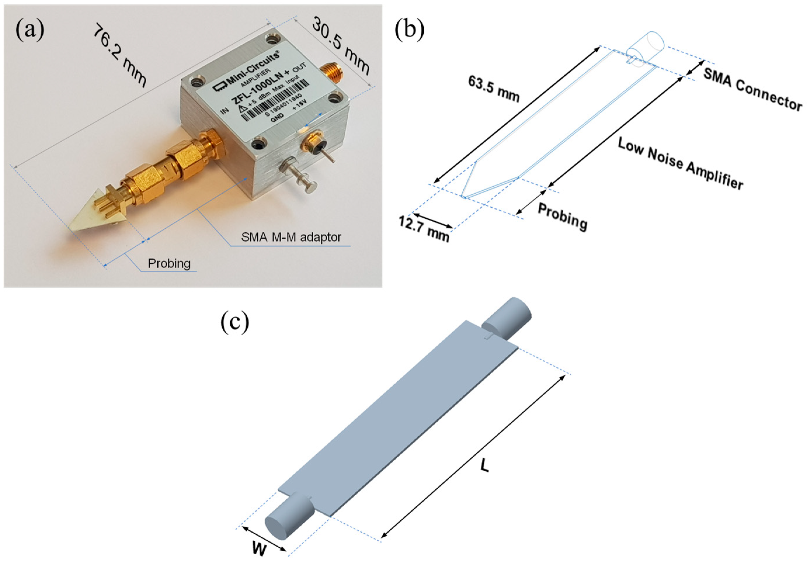
2.2. Microstrip Lines

The microstrip circuitization lines were carefully designed based on substrate properties to avoid unwanted reflections caused by impedance mismatch. Rogers® RO4350B was used as the substrate, reported to have a nominal dielectric constant of 3.66 and a loss tangent (tanδ) around 0.003 [25]. In order to obtain a characteristic impedance of 50 Ω, an optimal printed line width of 1.1 mm was simulated on a 0.5 mm thick substrate [26]. The size of the LNA is, however, relatively small compared to the operating wavelength of 30 cm (at the frequency of 1 GHz). The propagation loss is less than 1 dB for the application, as shown in Figure 3; therefore, the microstrip lines were accordingly designed to minimize reflections when printed on the RO4350B substrate. Based on the reflection coefficient of S21 in the scattering matrix, the transmitted power in the RF waveguide is expressed as follows:
P S 21 = exp 2 ( α d + α c ) z ,
where z is the length of the microstrip line and the two propagation coefficients, αd (dielectric attenuation) and αc (conductive loss), are related to the substrate loss and the skin depth of the microstrip lines, respectively [26]. The dielectric attenuation constant is linearly proportional to the loss tangent of the substrate, and the conductive loss coefficient is proportional to the square root of the resistivity of the conductor used for the microstrip lines. While the propagation loss of copper trace made by the conventional fabrication method is 0.03 dB/cm caused by high conductivity, the propagation loss of silver ink trace was simulated to be about 0.05 dB/cm, assuming that the resistivity of a commercially available nanoparticle-based silver ink is 5 times higher than that of bulk silver (ρAg = 1.6 × 10⁻⁸ Ω∙m) at 1 GHz, as shown in Figure 3 [27]. Note that the conductive loss is dominant over the dielectric attenuation, because of the use of a low loss substrate whose loss tangent is around 0.003. If the more popular FR-4 (a composite material composed of woven fiberglass with an epoxy resin binder) substrate material were used, the higher loss tangent of 0.03 would have resulted in a 10 times higher dielectric attenuation [28] due to the dielectric attenuation constant being linearly proportional to the loss tangent. Therefore, the use of an FR-4 substrate rather than the RO4350B would have resulted in a propagation loss larger than 0.1 dB/cm and the substrate loss from the dielectric attenuation would have dominated over the conductive loss caused by the finite resistivity of the silver ink.

3. Results and Discussion

As illustrated in Figure 4, both additive and subtractive manufacturing techniques were used for the fabrication of the proposed, high aspect ratio, LNA devices. First, the subtractive manufacturing steps were performed with an LPKF® S103 to cut the substrate to the correct size and drill the via holes. The LPKF machine has widely been used to make a PCB circuitization of Cu-plated substrates. In our case, a single-sided Cu-plated RO4350B substrate was used, where the Cu layer was used as a ground plane, so the LPKF has not been used for circuitization. The via holes were fabricated around the circuitization lines and unused substrate area to provide a stable ground connection and avoid RF leaks/interference from the signal lines [29]. The additive manufacturing steps were performed with a custom system fitted onto a HAAS® OM 2 computer numeric control (CNC) machine to fill the via holes. Subsequently, an Optomec® AJ200 was used to print the microstrip circuitization lines. The overall process steps for fabricating a single LNA device are highlighted in Figure 4, including: (1) substrate cut to size, (2) via holes drilled, (3) via holes filled with a silver paste using a syringe dispensing system, (4) two layers of conductive circuitization lines aerosol jet printed onto the substrate, (5) components mounted in their appropriate places using chip bonder (Loctite® 3621) as the adhesive, (6) components electrically connected to the circuitization lines using a syringe dispensed silver paste, and (7) connection of SMA connector to the fabricated LNA that is then mounted into an aluminum shielding enclosure. Post-processing occurred after every step except for steps (1) and (2). The post-processing recipes, such as curing temperature and duration, were carried out as recommended by the ink manufacturers. The total fabrication time from step (1) to step (7), excluding post-process, was ~7 h.

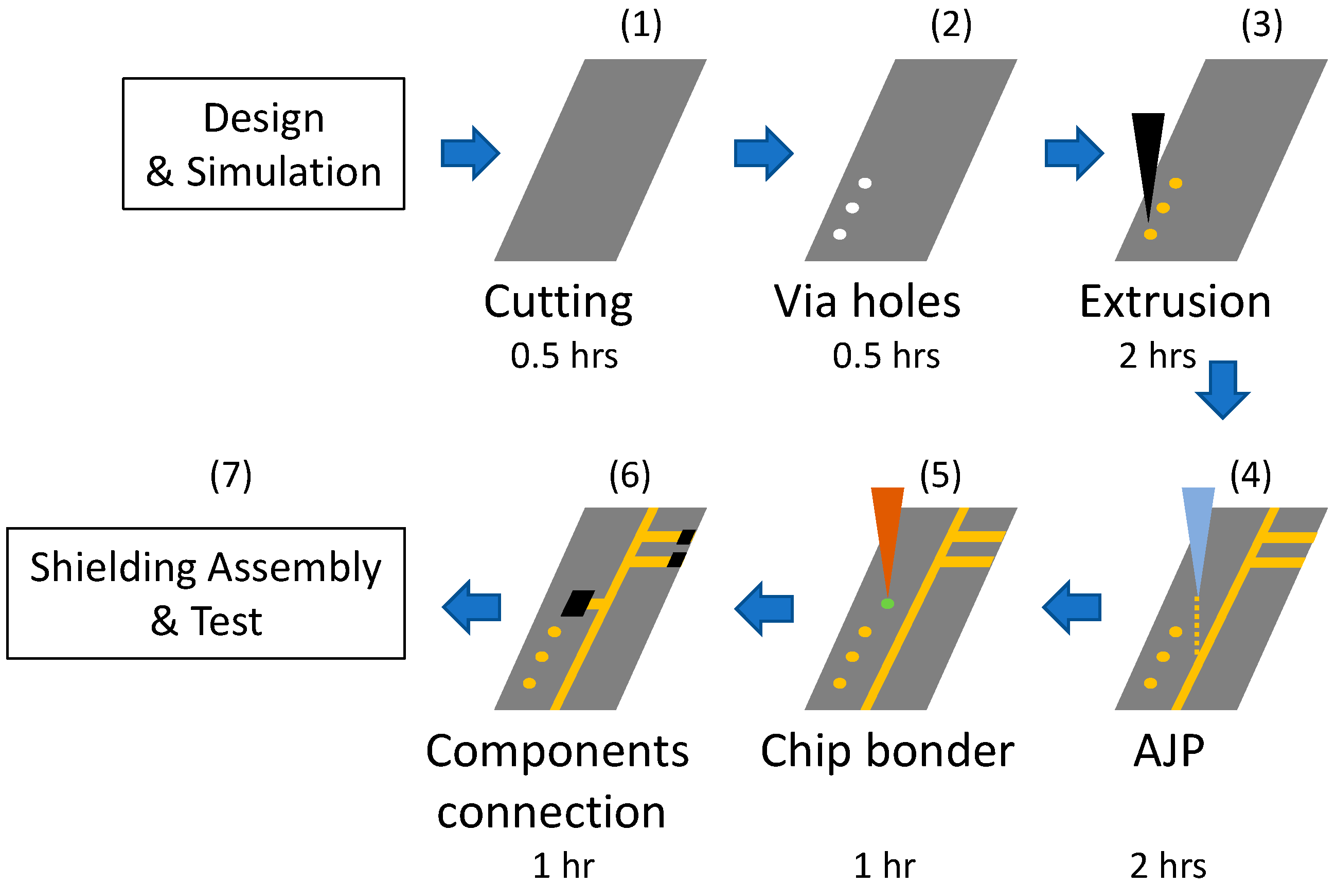
3.1. Via Holes and Extrusion-Based Syringe Printing

Initial prototyping and testing proved that using via hole fences was necessary to avoid RF leaks and interference. The same approach of via holes was used across all the three samples presented here. To create a via fence, an array of 0.7 mm diameter holes with a 1 mm center-to-center spacing was placed in open area sections of the substrate and along the ground circuitization lines. For the 5:1 aspect ratio LNA, close to 150 through-holes were drilled using the LPKF® ProtoMat S103 fitted with a 0.7 mm spiral drill. These holes were then filled with ACI FE3124 silver conductive paste (ACI Materials, Goleta, CA, USA) using a custom syringe printing attachment (Nordson EFD ValveMateTM 8000) on a HAAS® OM 2 vertical mill CNC machine [30]. A syringe tip with a 0.5 mm hole was placed directly over each via hole and pneumatic pressure applied for 1.5 s such that the extruded ink filled each hole. A dispensing pressure of around 60 psi was used, but varied slightly to ensure that the holes were adequately filled. The ground plane of the substrate was mounted face down for this process. Each hole was slightly overfilled in order to compensate for the shrinkage of the conductive paste due to solvent loss during post-process curing.

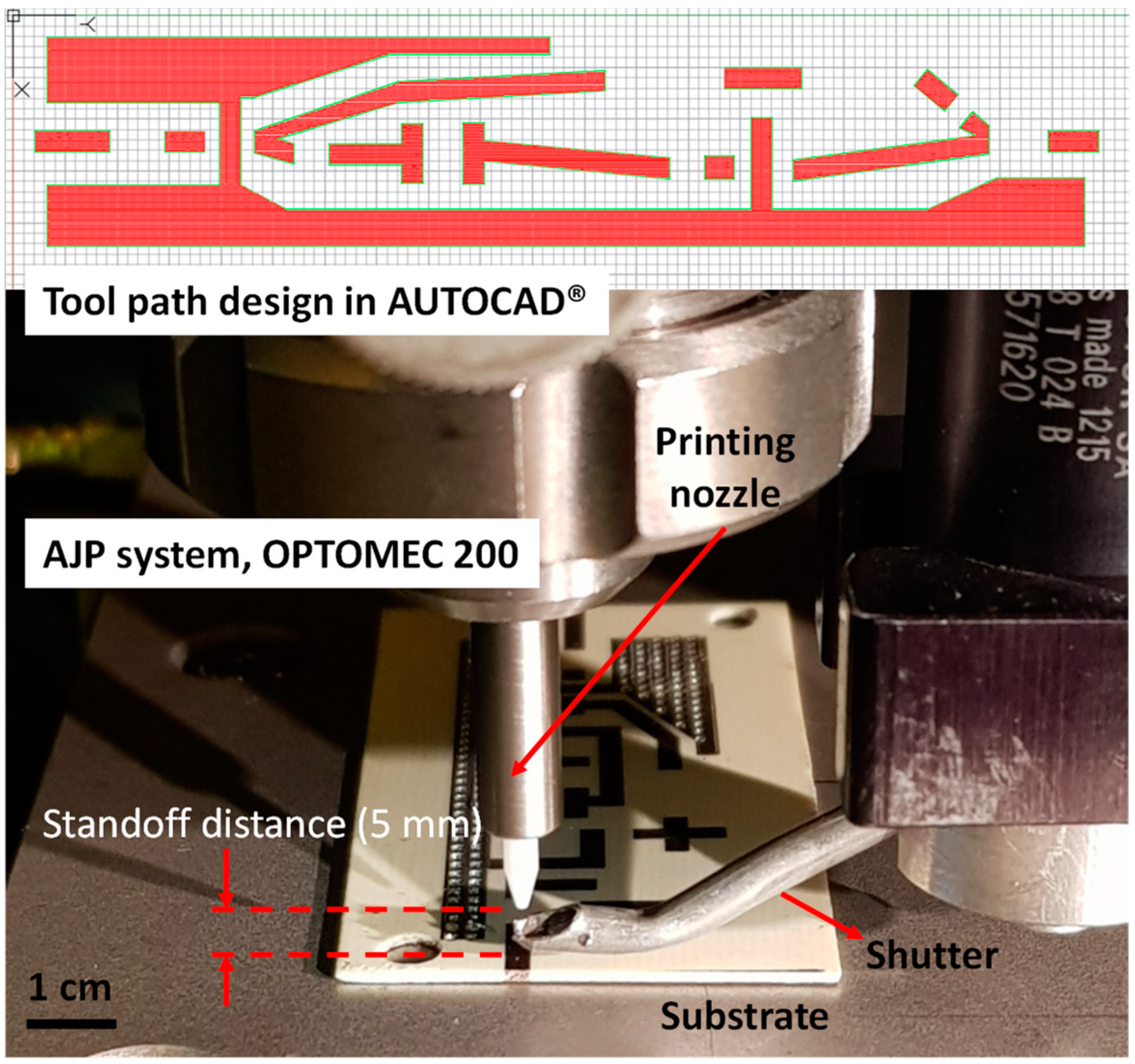
3.2. AJP Trace Printing

A direct write (DW) technology, aerosol jet printing (AJP) is well suited to print conductive and dielectric traces for RF applications [31,32] because it can be used to print a wide range of inks with viscosities from 1 to 1000 cps. Moreover, the relatively large stand-off distance (3–5 mm) offers advantages for conformal surface and complicated devices [33]. Stand-off distance and overlap of traces can have a significant impact on the quality and accuracy of the printed traces. A smaller stand-off distance can result in higher resolution and better control over the printed trace, but it can also decrease the overlap percentage between adjacent traces and increase the risk of clogging or damage to the nozzle. On the other hand, a larger stand-off distance can make it easier to print wider lines or cover a larger area with a higher overlap percentage, but it may result in lower resolution and less precise control. We optimize stand-off distance and overlap percentage for the specific requirements of the printing application, such as the desired resolution, thickness, and uniformity of the printed layer. Figure 5 shows the configuration of the AJP direct-write system used here. The circuit layout was designed using AUTOCAD® software and exported using an add-on software (VMtools) to create AJP toolpaths. DOWA (DOWA, Tokyo, Japan) conductive silver ink was used. Printed trace widths were set at 75 μm with a 50 μm serpentine fill pitch related to a 33% overlap of these printed traces with a serpentine pattern used to produce 1.1 mm wide printed circuitization lines. Two passes of the toolpath were used to decrease printing defects and achieve post-processed feature thicknesses of 10 μm. The build plate was heated to 50 °C to ensure solvents within the ink evaporated properly. Studies related to reliability, physics-of-failure, and adhesion with FR4 substrate have shown that high quality conductive traces can be obtained by controlling ink concentration and curing temperature [34,35,36]. The thermal procedure includes heating up in an oven from room temperature to 150 °C with a ramp rate of 2 °C/min, setting for 3 h, and subsequently cooling down in air. The substrate surface was further cleaned with isopropyl alcohol (IPA) prior to printing to improve adhesion. The printing nozzle diameter was 150 μm, and the print speed was 1–2 mm/s. In order to establish a printed trace width of 75 μm and an ink stream deposition rate of 0.0005 mm3/s, gas flows varied, but were typically set at 1100, 1070, and 15 sccm for the atomizer, exhaust, and sheath, respectively. The via holes that were previously filled with conductive paste were also over-printed in order to ensure that each via fence was properly connected between top and bottom substrate surfaces.
All the LNA circuitization lines were printed using a standard, commercially available nanoparticle-based silver ink (DOWA). The resistivity of the printed silver ink was measured using a four-point probe and found to be about five times bulk silver resistivity after post-processing at 150 °C for 3 h [27,37,38]. To control the layer thickness precisely, the inkwell method was used to establish desired deposition rates [37]. The target post-processed thickness of printed silver lines was set to be 10 µm, and a corresponding ink stream deposition rate of 0.0005 mm3/sec was used during printing. The surface roughnesses of the printed trace and the substrate were less than 1.5 μm and 3 μm, respectively. The printing and fabrication parameters are listed in Table 2. While these specific prototype parts have not undergone reliability testing, the materials used to fabricate these parts have undergone materials physics-of-failure testing [35,36] and other related additively fabricated circuits have been through [39] and are currently undergoing comprehensive reliability testing.

3.3. AJP Trace Printing Shielding and Assembly

Due to the focus on rapid production and the unavailability of an automated pick-and-place (PnP) tool, components were placed on the board by hand with tweezers. A small amount of chip bonder was used to secure these components in place. After the chip bonder was cured, each component was electrically connected to the printed circuitization using ACI FE3124 silver conductive paste. This paste was applied with a syringe by hand. The manual method for both the component placement and electrical connection to circuitization lines can easily be replaced by a programmed PnP process and syringe printing for higher precision placement and mass production. The fully fabricated LNA was placed in an aluminum shielding mount where the ground plane was in contact with the mount. The shielding structure not only provides a stable ground plane, but also secure connections between the input/output traces and SMA connectors in order to avoid electrical disconnection caused by any torque exerted while attaching the SMA connectors.

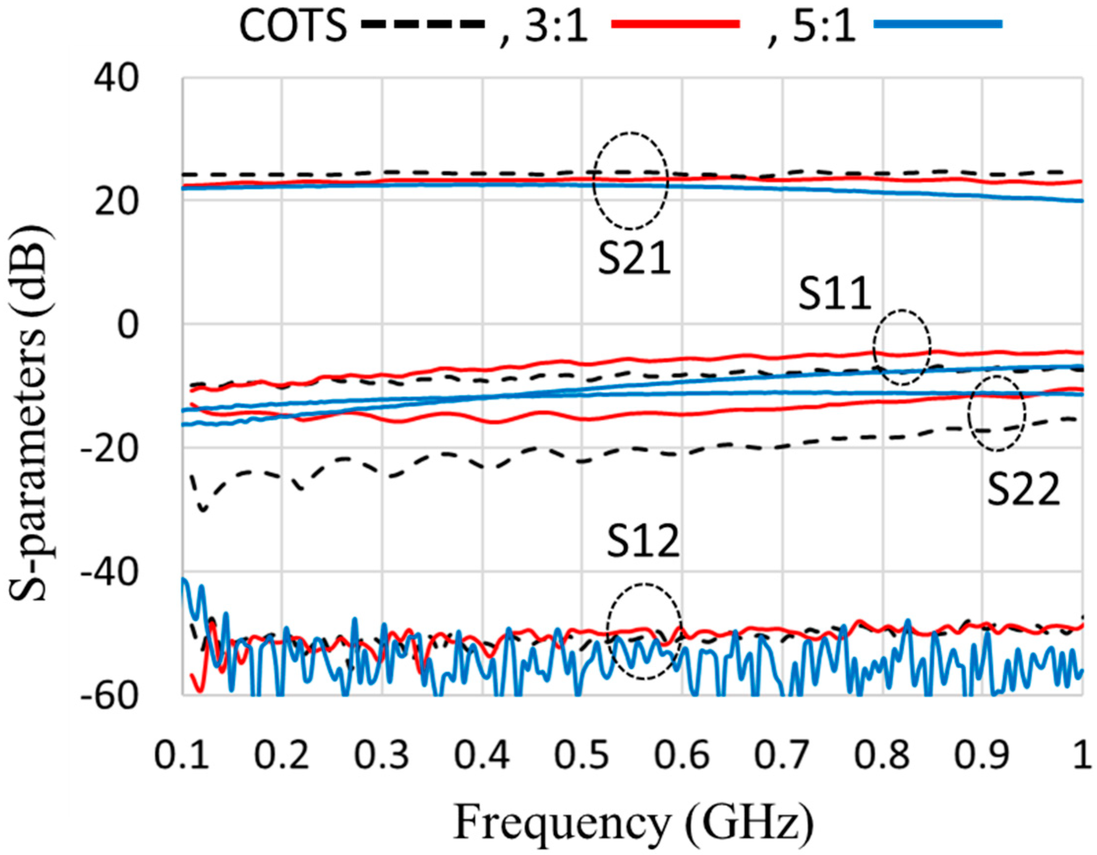
3.4. Experimental Results

Gain and NF measurements were performed to confirm the feasibility of low noise amplification from the fabricated high aspect ratio LNAs. The DC power supply was set at 15.31 volts to LNA and the signal of the RF input was fixed to −60 dBm from an Agilent® 4420B signal generator. The amplified spectrum was measured by an Anritsu MS2690A signal analyzer. The signal analyzer was calibrated with the amplitude, and the phase error was less than 0.5 dB. The high frequency SMA cables were used for input and output connection, where the insertion loss is expected to be less than 1 dB at 1 GHz. Figure 6 shows measured gain and NF as a function of frequency with data from the commercial LNA (gray line) for comparison. A simple gain method is used to measure NF by comparing the noise floor with the Johnson–Nyquist noise at room temperature [40].
The measured gain for the highest ratio (5:1) printed LNA was around 25 dB, ~2 dB higher than the COTS LNA [24], where the gain of the COTS LNA has separately been measured for comparison. The lower aspect ratio (1:1) LNA shows a slight roll-off in gain at the higher frequency, whereas the higher aspect ratio (5:1 printed prototype) LNA has a relatively flat gain profile with a broadband frequency up to 1 GHz, which is ideal for most broadband amplifier operations. The slight decrease in the gain is believed to result from the relatively long traces but could also be related to micro-cracking in the silver traces that are potential known defects that can form as a result of multiple cures for silver ink and chip bonder. Note that the simulated gain from ADS (green line) shows a good agreement with the experimental result over the frequency range of interest. The measured NF of the 5:1 aspect ratio LNA was around 3 dB, which is lower than that of the COTS LNA, over most of the measured frequency range. We expect that the low NF will help to increase the sensitivity of active handheld sensor devices. Using a vector network analyzer (Rohde & Schwarz ZVA67A), a reverse isolation, equivalent to S12, was separately measured to be less than −40 dB within all frequencies up to 1 GHz.
Figure 7 shows the full S-parameters of the 3:1 and 5:1 aspect ratio LNAs and COTS devices as measured using an Agilent N5230A Vector Network Analyzer. The forward and backward transmission coefficients (S21 and S12) were about 20–23 dB and −50 dB, respectively. The S12 of −50 dB represented very high isolation/rejection in the output port, which is crucial for amplifier design. The forward and backward reflection coefficients (S11 and S22) ranged from −30 dB to −10 dB up to a frequency of 1 GHz.

4. Conclusions

We have successfully demonstrated rapid prototyping of a high aspect ratio LNA for an active handheld sensor device operating up to 1 GHz using additive and subtractive manufacturing technologies. Both high gain and a low NF are important factors to secure high signal integrity in all sensor applications without a large increase in noise level. The gain and NF obtained from the fabricated prototype LNAs were comparable with the COTS LNA products. The integration of sensors with the proposed small form factor LNA will be expected to be useful for active handheld probing devices. We believe our approach can be applied to other types of RF passive electronic or bio-sensors by simple modification and integration of the LNA as presented in this paper, not only to show a proof of concept, but also to create a novel active handheld sensor device where signals of very low strength need to be amplified.

Author Contributions

Conceptualization, D.R.H.; methodology, A.C.-P., C.Y. and D.P.; software, A.P and D.P.; validation, A.C.-P., D.P., D.E. and D.R.H.; formal analysis, D.P.; investigation, D.E.; resources, D.R.H.; data curation, D.P.; writing—original draft preparation, D.P.; writing—review and editing, A.C.-P., C.Y., D.P., D.E., D.K. and D.R.H.; visualization, D.P.; supervision, D.R.H.; project administration, D.K.; All authors have read and agreed to the published version of the manuscript.

Funding

This research received no external funding.

Data Availability Statement

Data available upon request.

Acknowledgments

We thank Philip Li and Jason Fleischer for help with the experimental setup, the fabrication, and the suggestions.

Conflicts of Interest

The authors declare no conflict of interest.

References

  1. Zastrow, M. 3D Printing Gets Bigger, Faster and Stronger. Nature 2020, 578, 20–23. [Google Scholar] [CrossRef] [PubMed]
  2. Macdonald, E.; Salas, R.; Espalin, D.; Perez, M.; Aguilera, E.; Muse, D.; Wicker, R.B. 3D Printing for the Rapid Prototyping of Structural Electronics. IEEE Access 2014, 2, 234–242. [Google Scholar] [CrossRef]
  3. Eid, A.; He, X.; Bahr, R.; Lin, T.-H.; Cui, Y.; Adeyeye, A.; Tehrani, B.; Tentzeris, M.M. Inkjet-/3D-/4D-Printed Perpetual Electronics and Modules: RF and Mm-Wave Devices for 5G+, IoT, Smart Agriculture, and Smart Cities Applications. IEEE Microw. Mag. 2020, 21, 87–103. [Google Scholar] [CrossRef]
  4. Calignano, F.; Manfredi, D.; Ambrosio, E.P.; Biamino, S.; Lombardi, M.; Atzeni, E.; Salmi, A.; Minetola, P.; Iuliano, L.; Fino, P. Overview on Additive Manufacturing Technologies. Proc. IEEE 2017, 105, 593–612. [Google Scholar] [CrossRef]
  5. Kim, C.; Espalin, D.; Liang, M.; Xin, H.; Cuaron, A.; Varela, I.; Macdonald, E.; Wicker, R.B. 3D Printed Electronics with High Performance, Multi-Layered Electrical Interconnect. IEEE Access 2017, 5, 25286–25294. [Google Scholar] [CrossRef]
  6. Eshkeiti, A.; Reddy, A.S.G.; Emamian, S.; Narakathu, B.B.; Joyce, M.; Joyce, M.; Fleming, P.D.; Bazuin, B.J.; Atashbar, M.Z. Screen Printing of Multilayered Hybrid Printed Circuit Boards on Different Substrates. IEEE Trans. Comp. Packag. Manuf. Technol. 2015, 5, 415–421. [Google Scholar] [CrossRef]
  7. Attaran, M. The Rise of 3-D Printing: The Advantages of Additive Manufacturing over Traditional Manufacturing. Bus. Horiz. 2017, 60, 677–688. [Google Scholar] [CrossRef]
  8. Shin, K.-H.; Nguyen, H.A.D.; Park, J.; Shin, D.; Lee, D. Roll-to-Roll Gravure Printing of Thick-Film Silver Electrode Micropatterns for Flexible Printed Circuit Board. J. Coat. Technol. Res. 2017, 14, 95–106. [Google Scholar] [CrossRef]
  9. Tavakoli, M.; Malakooti, M.H.; Paisana, H.; Ohm, Y.; Marques, D.G.; Lopes, P.A.; Piedade, A.P.; de Almeida, A.T.; Majidi, C. EGaIn-Assisted Room-Temperature Sintering of Silver Nanoparticles for Stretchable, Inkjet-Printed, Thin-Film Electronics. Adv. Mater. 2018, 30, 1801852. [Google Scholar] [CrossRef]
  10. Cai, F.; Ulusoy, A.Ç.; Papapolymerou, J. 2.4 GHz Low Cost Low Noise Amplifier on Flexible Organic Substrate. In Proceedings of the 2013 Asia-Pacific Microwave Conference Proceedings (APMC), Seoul, Republic of Korea, 5–8 November 2013; pp. 270–272. [Google Scholar] [CrossRef]
  11. Oakley, C.R. Additive Manufacturing for RF Electronics Packaging; Michigan State University: East Lansing, MI, USA, 2020. [Google Scholar] [CrossRef]
  12. Oakley, C.; Chahal, P.; Papapolymerou, J.; Albrecht, J.D. Fabrication of X-Band Oscillator on LCP Substrate Using Aerosol Printing. Int. Symp. Microelectron. 2017, 2017, 52–55. [Google Scholar] [CrossRef]
  13. Mohd Ghazali, M.I.; Karuppuswami, S.; Mondal, S.; Chahal, P. Embedded Active Elements in 3D Printed Structures for the Design of RF Circuits. In Proceedings of the 2018 IEEE 68th Electronic Components and Technology Conference (ECTC), San Diego, CA, USA, 29 May–1 June 2018; pp. 1062–1067. [Google Scholar] [CrossRef]
  14. Ketterl, T.P.; Vega, Y.; Arnal, N.C.; Stratton, J.W.I.; Rojas-Nastrucci, E.A.; Córdoba-Erazo, M.F.; Abdin, M.M.; Perkowski, C.W.; Deffenbaugh, P.I.; Church, K.H.; et al. A 2.45 GHz Phased Array Antenna Unit Cell Fabricated Using 3-D Multi-Layer Direct Digital Manufacturing. IEEE Trans. Microw. Theory Tech. 2015, 63, 4382–4394. [Google Scholar] [CrossRef]
  15. Cook, B.S.; Tehrani, B.; Cooper, J.R.; Tentzeris, M.M. Multilayer Inkjet Printing of Millimeter-Wave Proximity-Fed Patch Arrays on Flexible Substrates. IEEE Antennas Wirel. Propag. Lett. 2013, 12, 1351–1354. [Google Scholar] [CrossRef]
  16. Friel, R.J.; Gerling-Gerdin, M.; Nilsson, E.; Andreasson, B.P. 3D Printed Radar Lenses with Anti-Reflective Structures. Designs 2019, 3, 28. [Google Scholar] [CrossRef]
  17. Deffenbaugh, P.I.; Weller, T.M.; Church, K.H. Fabrication and Microwave Characterization of 3-D Printed Transmission Lines. IEEE Microw. Wirel. Compon. Lett. 2015, 25, 823–825. [Google Scholar] [CrossRef]
  18. Williams, C.C.; Wickramasinghe, H.K. Scanning Thermal Profiler. Appl. Phys. Lett. 1986, 49, 1587. [Google Scholar] [CrossRef]
  19. Li, G.; Pommerenke, D.; Min, J. A Low Frequency Electric Field Probe for Near-Field Measurement in EMC Applications. In Proceedings of the 2017 IEEE International Symposium on Electromagnetic Compatibility Signal/Power Integrity (EMCSI), Washington DC, USA, 7–11 August 2017; pp. 498–503. [Google Scholar] [CrossRef]
  20. Wang, J.; Yan, Z.; Liu, W.; Su, D.; Yan, X. A Novel Tangential Electric-Field Sensor Based on Electric Dipole and Integrated Balun for the Near-Field Measurement Covering GPS Band. Sensors 2019, 19, 1970. [Google Scholar] [CrossRef]
  21. Shaeffer, D.K.; Lee, T.H. A 1.5-V, 1.5-GHz CMOS Low Noise Amplifier. IEEE J. Solid-State Circuits 1997, 32, 745–759. [Google Scholar] [CrossRef]
  22. Zhou, N.; Liu, C.; Lewis, J.A.; Ham, D. Gigahertz Electromagnetic Structures via Direct Ink Writing for Radio-Frequency Oscillator and Transmitter Applications. Adv. Mater. 2017, 29, 1605198. [Google Scholar] [CrossRef]
  23. Paolella, A.C.; Silva-Saez, D.; Kozlovski, D.; Even, R. 3-D Printed RF Amplifier for Wireless Systems. In Proceedings of the 2019 IEEE Radio and Wireless Symposium (RWS), Orlando, FL, USA, 20–23 January 2019; pp. 1–3. [Google Scholar] [CrossRef]
  24. Mini-Circuits®. Available online: https://www.minicircuits.com/pdfs/ZFL-1000LN+.pdf (accessed on 15 November 2022).
  25. Available online: https://rogerscorp.com/advanced-connectivity-solutions/ro4000-series-laminates/ro4350b-laminates (accessed on 15 November 2022).
  26. Pozar, D.M. Microwave Engineering, 4th ed.; Wiley: Hoboken, NJ, USA, 2011; ISBN 978-0-470-63155-3. [Google Scholar]
  27. Gu, Y.; Hines, D.R.; Yun, V.; Antoniak, M.; Das, S. Aerosol-Jet Printed Fillets for Well-Formed Electrical Connections between Different Leveled Surfaces. Adv. Mater. Technol. 2017, 2, 1700178. [Google Scholar] [CrossRef]
  28. Djordjevic, A.R.; Biljie, R.M.; Likar-Smiljanic, V.D.; Sarkar, T.K. Wideband Frequency-Domain Characterization of FR-4 and Time-Domain Causality. IEEE Trans. Electromagn. Compat. 2001, 43, 662–667. [Google Scholar] [CrossRef]
  29. El Gibari, M.; Li, H. A Comparative Study between Via-Hole and Via-Free Grounded Coplanar Waveguide to Microstrip Transitions on Thin Polymer Substrate. Available online: https://www.hindawi.com/journals/ijap/2015/481768/ (accessed on 19 October 2020).
  30. HAAS CNC. Available online: https://www.haascnc.com/machines/vertical-mills.html (accessed on 15 November 2022).
  31. Gupta, A.A.; Soer, M.C.M.; Taherzadeh-Sani, M.; Cloutier, S.G.; Izquierdo, R. Aerosol-Jet Printed Transmission Lines for Microwave Packaging Applications. IEEE Trans. Comp. Packag. Manuf. Technol. 2019, 9, 2482–2489. [Google Scholar] [CrossRef]
  32. Qayyum, J.A.; Abt, M.; Roch, A.; Ulusoy, A.C.; Papapolymerou, J. Ultra Wideband 3D Interconnects Using Aerosol Jet Printing up to 110 GHz. In Proceedings of the 2017 47th European Microwave Conference (EuMC), Nuremberg, Germany, 10–12 October 2017; pp. 1112–1115. [Google Scholar] [CrossRef]
  33. King, B.; Renn, M. Aerosol Jet® Direct Write Printing for Mil-Aero Electronic Applications. Available online: https://www.optomec.com/wp-content/uploads/2014/04/Optomec_Aerosol_Jet_Direct_Write_Printing_for_Mil_Aero_Electronic_Apps.pdf (accessed on 15 November 2022).
  34. Hung, K.-Y.; Chang, Y.-T.; Chien, C.-H.; Ding, C.-F.; Tsai, M.-C.; Young, H.-T. Investigation of Ink Modification for Aerosol Jet Printing Process on FR-4 Substrate. Int. J. Adv. Manuf. Technol. 2020, 111, 1147–1156. [Google Scholar] [CrossRef]
  35. Dalal, N.; Gu, Y.; Chen, G.; Hines, D.R.; Dasgupta, A.; Das, S. Effect of Gas Flow Rates on Quality of Aerosol Jet Printed Traces with Nanoparticle Conducting Ink. J. Electron. Packag. 2019, 142, 011012. [Google Scholar] [CrossRef]
  36. Dalal, N.; Gu, Y.; Hines, D.R.; Dasgupta, A.; Das, S. Cracks in the 3D-Printed Conductive Traces of Silver Nanoparticle Ink. J. Micromech. Microeng. 2019, 29, 097001. [Google Scholar] [CrossRef]
  37. Gu, Y.; Gutierrez, D.; Das, S.; Hines, D.R. Inkwells for On-Demand Deposition Rate Measurement in Aerosol-Jet Based 3D Printing. J. Micromech. Microeng. 2017, 27, 097001. [Google Scholar] [CrossRef]
  38. Gu, Y.; Park, D.; Gonya, S.; Jendrisak, J.; Das, S.; Hines, D.R. Direct-Write Printed Broadband Inductors. Addit. Manuf. 2019, 30, 100843. [Google Scholar] [CrossRef]
  39. Bolger, J.; Lantz, L.; Lewis, R.; Trudeau, R.; Hines, D. Multi-Layer PC Boards Fabricated Using Aerosol-Jet Printing. Int. Symp. Microelectron. 2013, 2013, 921–926. [Google Scholar] [CrossRef]
  40. Friis, H.T. Noise Figures of Radio Receivers. Proc. IRE 1944, 32, 419–422. [Google Scholar] [CrossRef]
Figure 1. (a) Example of EMC probing sensor with a COTS LNA from Mini-Circuits®. (b) Schematic of a high aspect ratio (5:1) active near-field probing sensor (LNA + probe). (c) Schematic of a proposed LNA with two SMA connections for input and output. Length (L) and width (W) are varied for different aspect ratios.
Jmmp 07 00083 g001
Figure 2. (a) 3:1 circuit schematic for simulation and fabrication. FET3 and FET6 are Mini-Circuits® MAR-3SM+ and MAR-6SM+, respectively. (b) Mini-Circuits® ZFL-1000LN+. (c) 1:1, (d) 3:1, and (e) 5:1 aspect ratio printed LNAs and packaged with shielding and SMA connectors.
Jmmp 07 00083 g002
Figure 3. Transmitted power with varying length of transmission line. The dotted, dashed, and solid lines are transmitted powers caused by dielectric attenuation (substrate loss), conductive loss (skin depth), and both effects, respectively, at 1 GHz, assuming that the silver ink has 5 times higher resistivity than bulk silver. The red data point with the error bar is from separate S21 measurement of the 2.5 cm long AJP transmission line at 1 GHz. Inset shows S21 of the 2.5 cm long AJP transmission line as a function of frequency up to 1 GHz. At 1 GHz, the S21 was around −0.17 dB.
Jmmp 07 00083 g003
Figure 4. Schematic illustrations of the fabrication procedure for the LNA. (1) Cutting the bulk RO4350B substrate and (2) making via holes using the LPKF® ProtoMat S103, (3) filling the holes with extrusion of silver paste, (4) AJP for conductive circuitization lines, (5) chip bonder dispensing for SMD placement, (6) components placement, and (7) shielding assembly for RF test.
Jmmp 07 00083 g004
Figure 5. AJP system (OPTOMEC 200) used for the high aspect ratio LNA, and (top) an example of a tool path generated in AUTOCAD®.
Jmmp 07 00083 g005
Figure 6. Gain and NF vs. frequency. The gray line and dashed line are the gain and NF of the COTS LNA, respectively. The green line and dashed gray lines are the gain and NF from the ADS circuit simulation, respectively.
Jmmp 07 00083 g006
Figure 7. S-parameters of COTS (dashed), 3:1 aspect ratio LNA (red line), and 5:1 aspect ratio LNA (blue line) with the bias voltage of 15 V, 15 V, and 16 V, respectively. The bias currents for all the measurement were ~50 mA.
Jmmp 07 00083 g007
Table 1. Examples of 3D printed RF devices.
TypeAM 1
Method
Performance/InformationFrequency (GHz)
LNA [10]AJP 1G = 12 dB2.4
Oscillator [11,12]AJPBW = 0.3 GHz10
T-line resonator [13]SLA 1Varactor used4.5–6.5
Phased array antenna [14]FDM 1G = −11 dBi2.45
Patch antenna [15]InkjetBW = 0.8 GHz24.5
RF lens [16]FDMBroadband60
Transmission line [17]SyringeBroadband10
1 AM (additive manufacturing), AJP (aerosol jet printing), SLA (stereolithography), FDM (fused deposition method).
Table 2. Important parameters for printing and fabrication.
ParametersUnitValue
Thickness of substratemm0.5
Circuitization widthmm1.1
Diameter of viaμm700
Deposition rate of ink streammm3/s0.0005
Print speedmm/s1–2
Fill pitch between printed tracesμm50
Printed trace widthμm75
Thickness of circuitizationμm10
Stand-off distance (AJP)mm3–5
Curing temp. of DOWA°C150
Curing time of DOWAhours3
Curing temp. of chip bonder°C100
Curing time of chip bonderhours1
Disclaimer/Publisher’s Note: The statements, opinions and data contained in all publications are solely those of the individual author(s) and contributor(s) and not of MDPI and/or the editor(s). MDPI and/or the editor(s) disclaim responsibility for any injury to people or property resulting from any ideas, methods, instructions or products referred to in the content.

