

Quenching Circuit Discriminator Architecture Impact on a Sub-10 ps FWHM Single-Photon Timing Resolution SPAD
 , , , and
Abstract
:1. Introduction
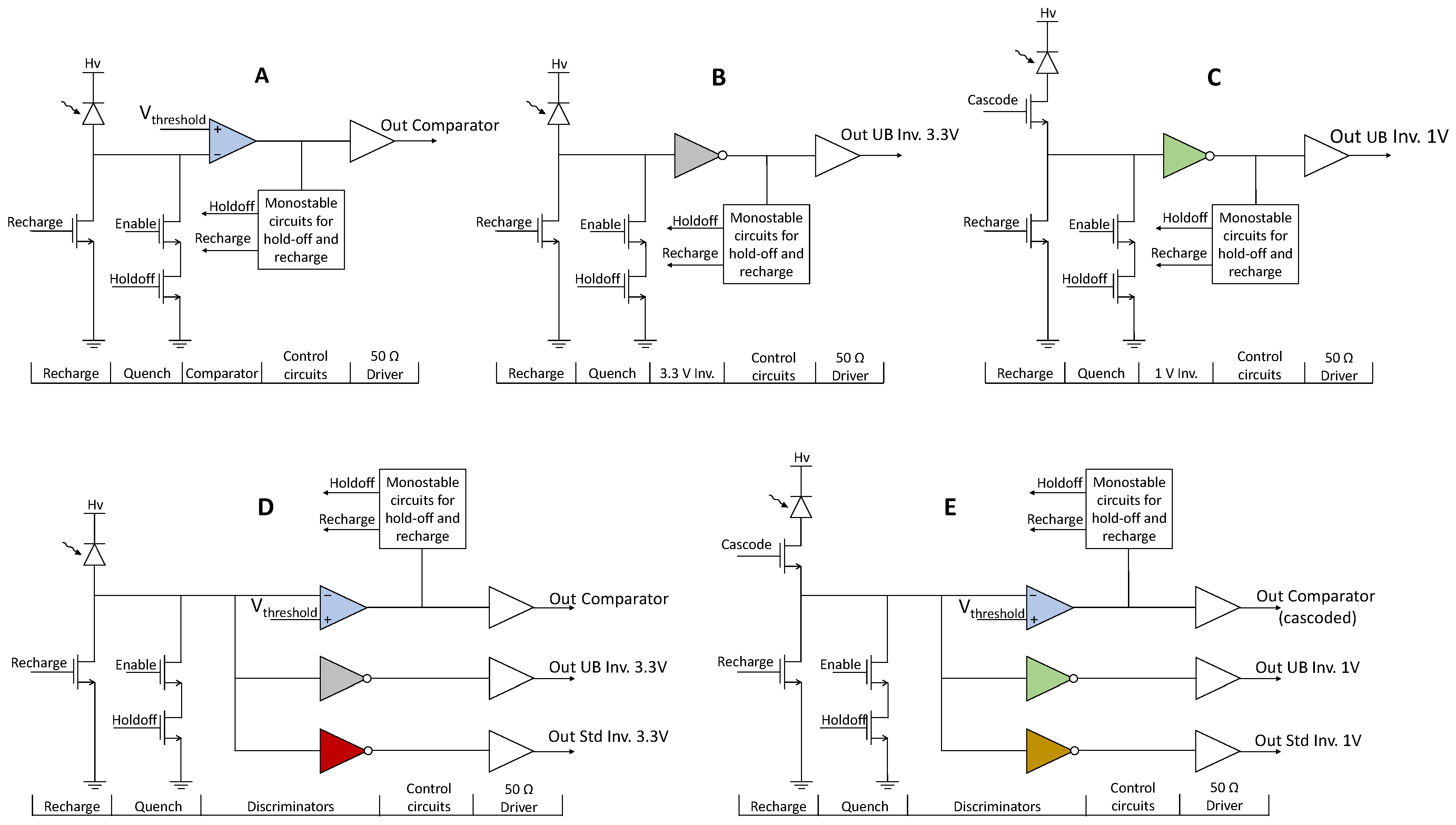
2. Architecture
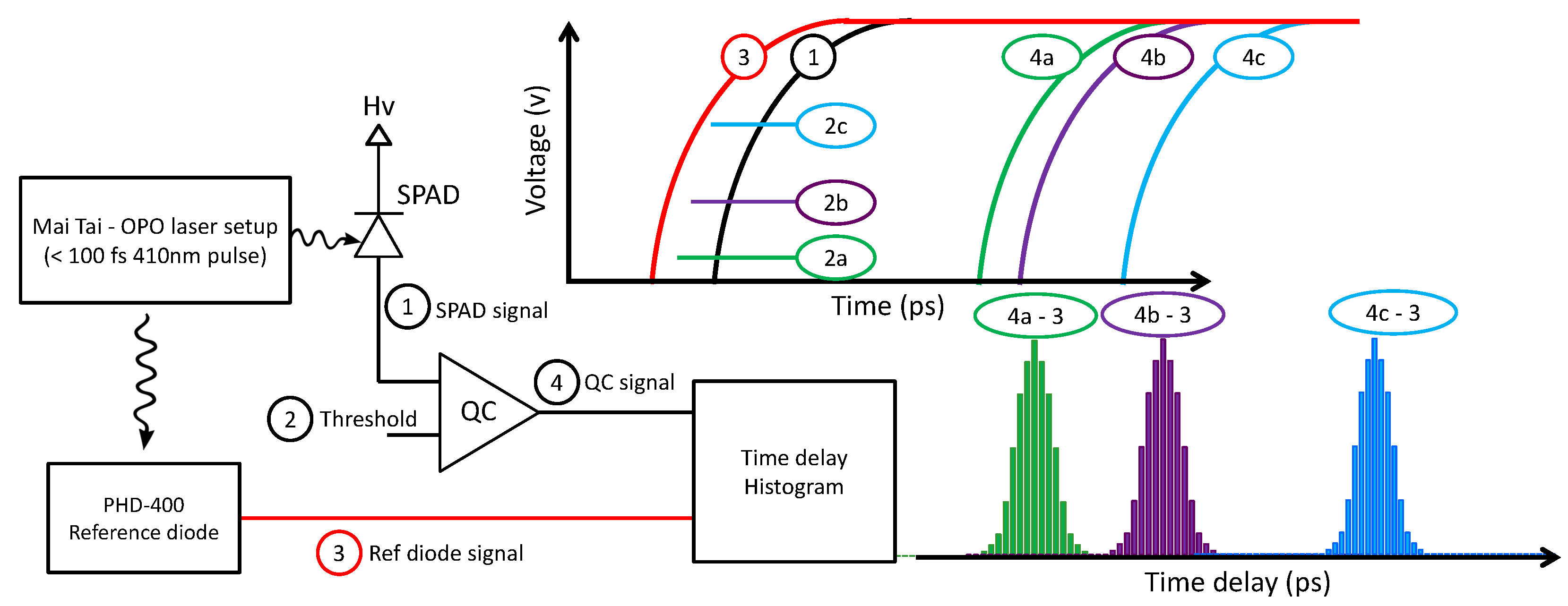
3. Materials and Methods
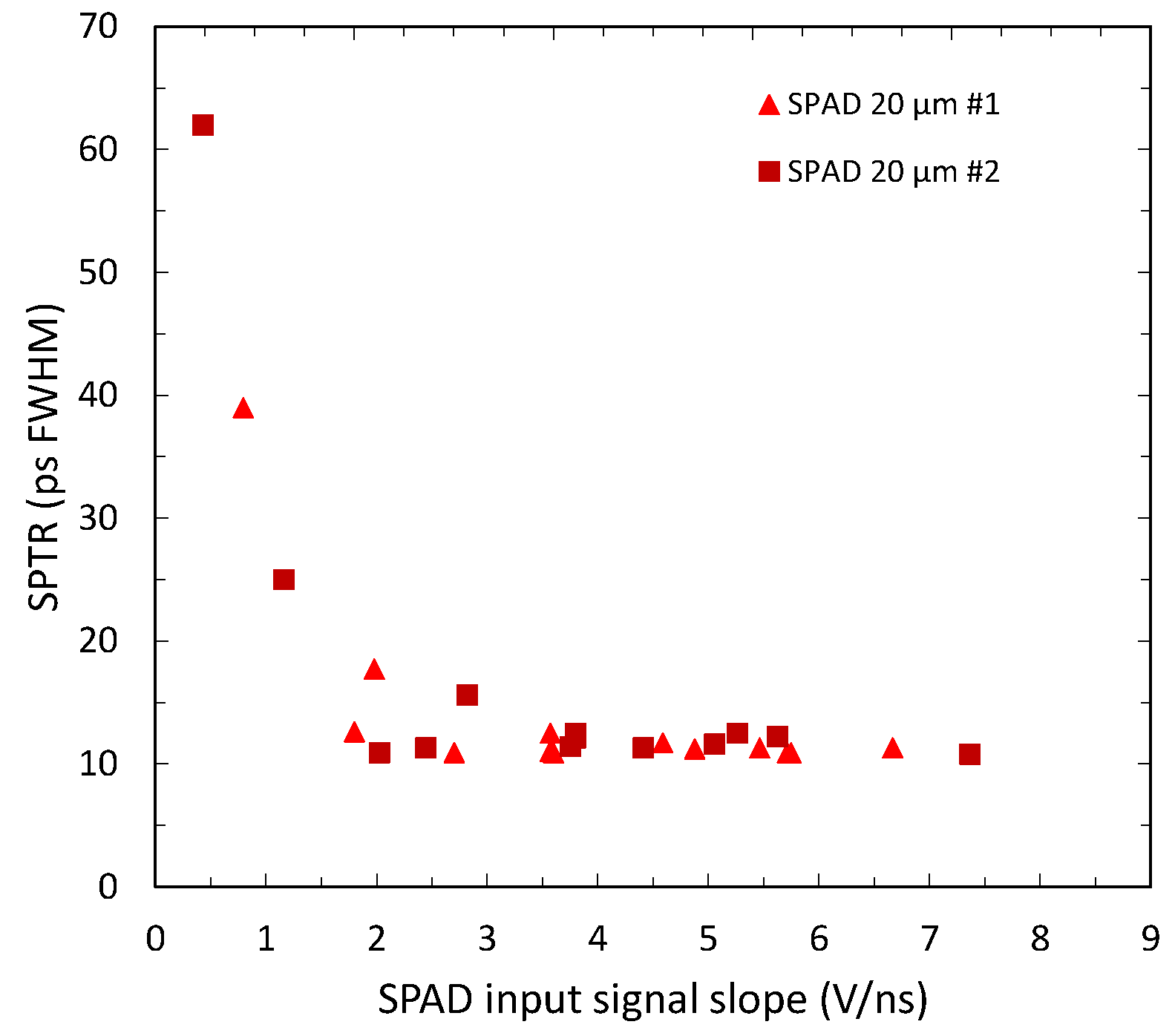
3.1. Discriminator’s Input Signal Slope
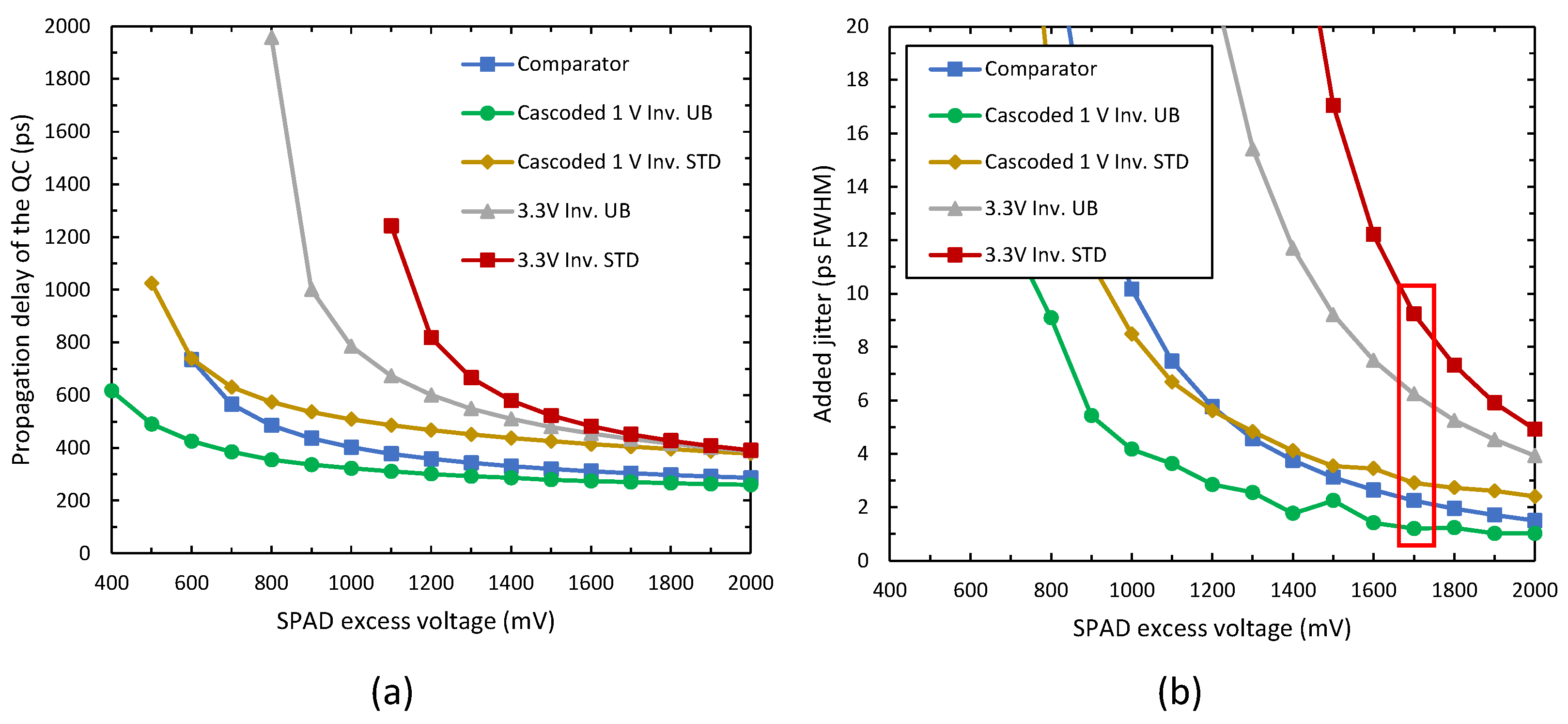
3.2. Overdrive Variation Jitter
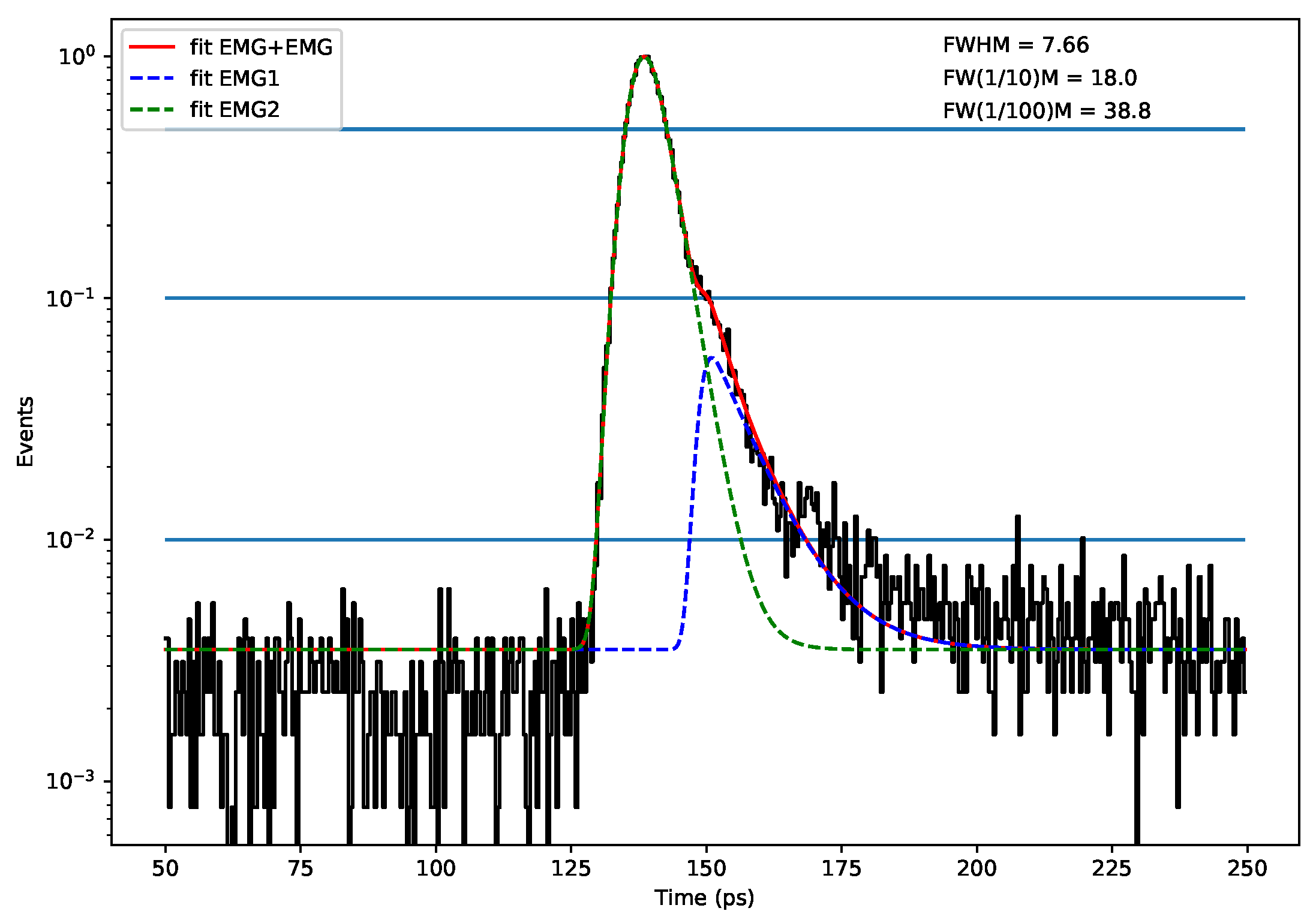
3.3. Single-Photon Timing Resolution
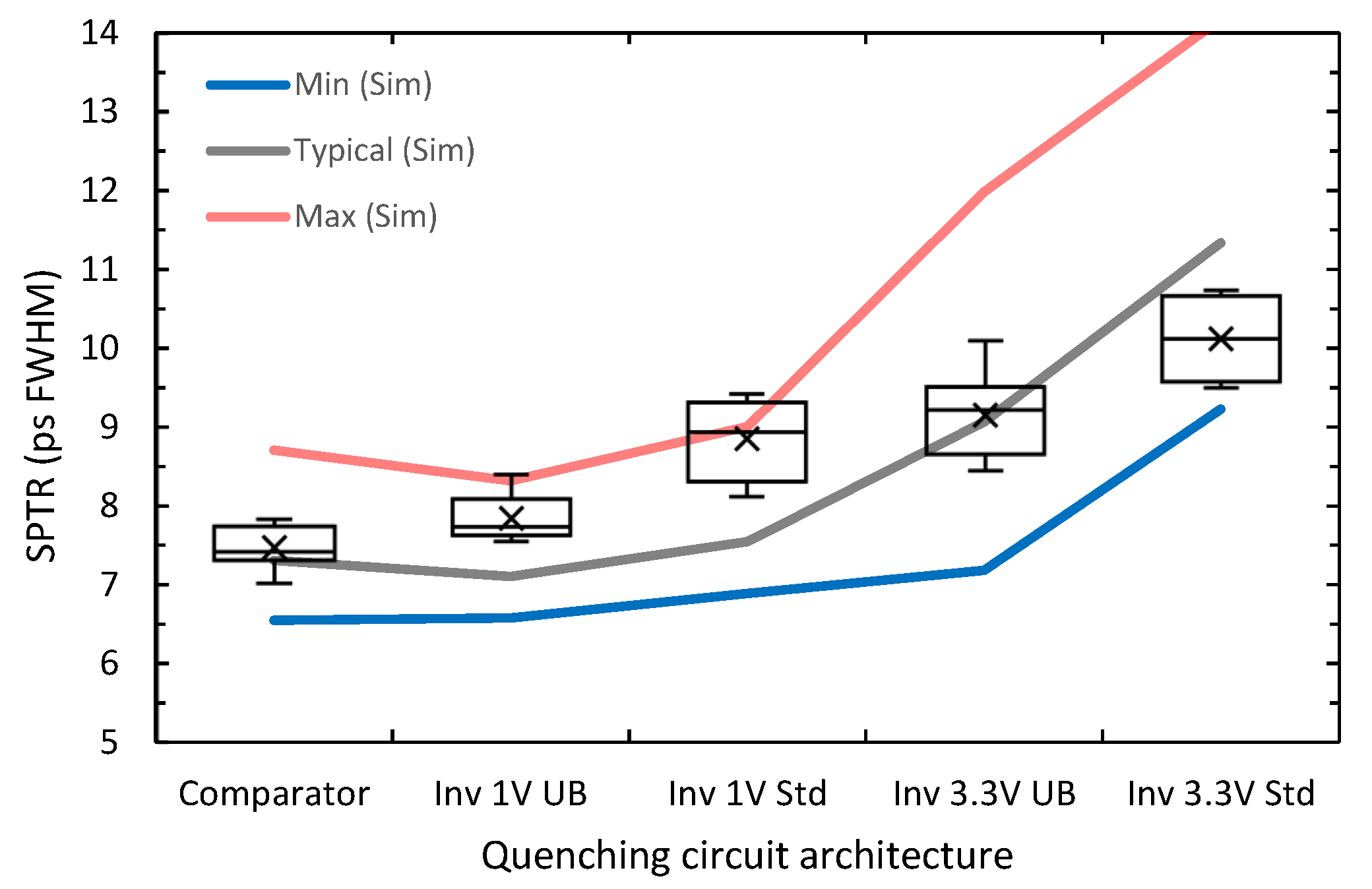
3.4. Cascode Architecture Impact on the SPTR
4. Results
4.1. SPAD Characteristics
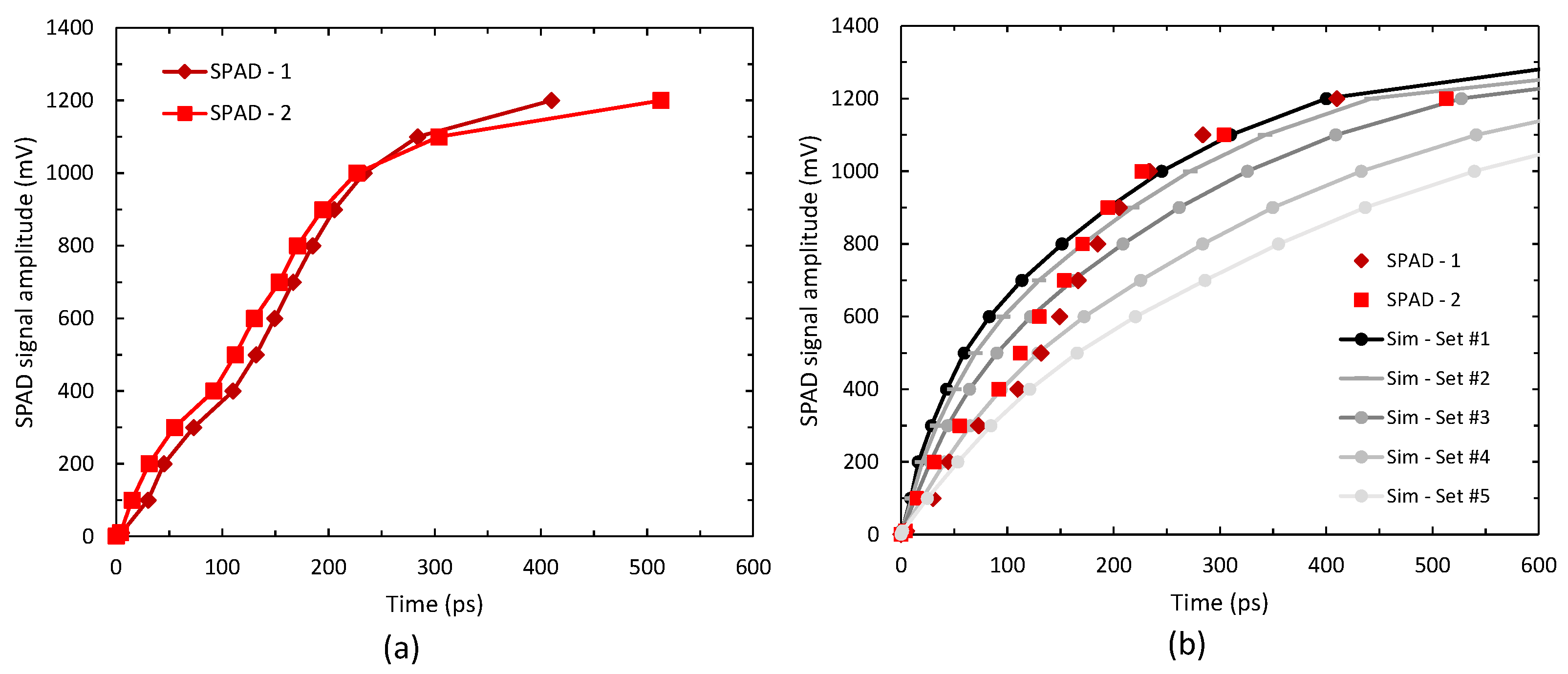
4.2. Discriminator’s Input Signal Slope
4.3. Overdrive Variation Jitter
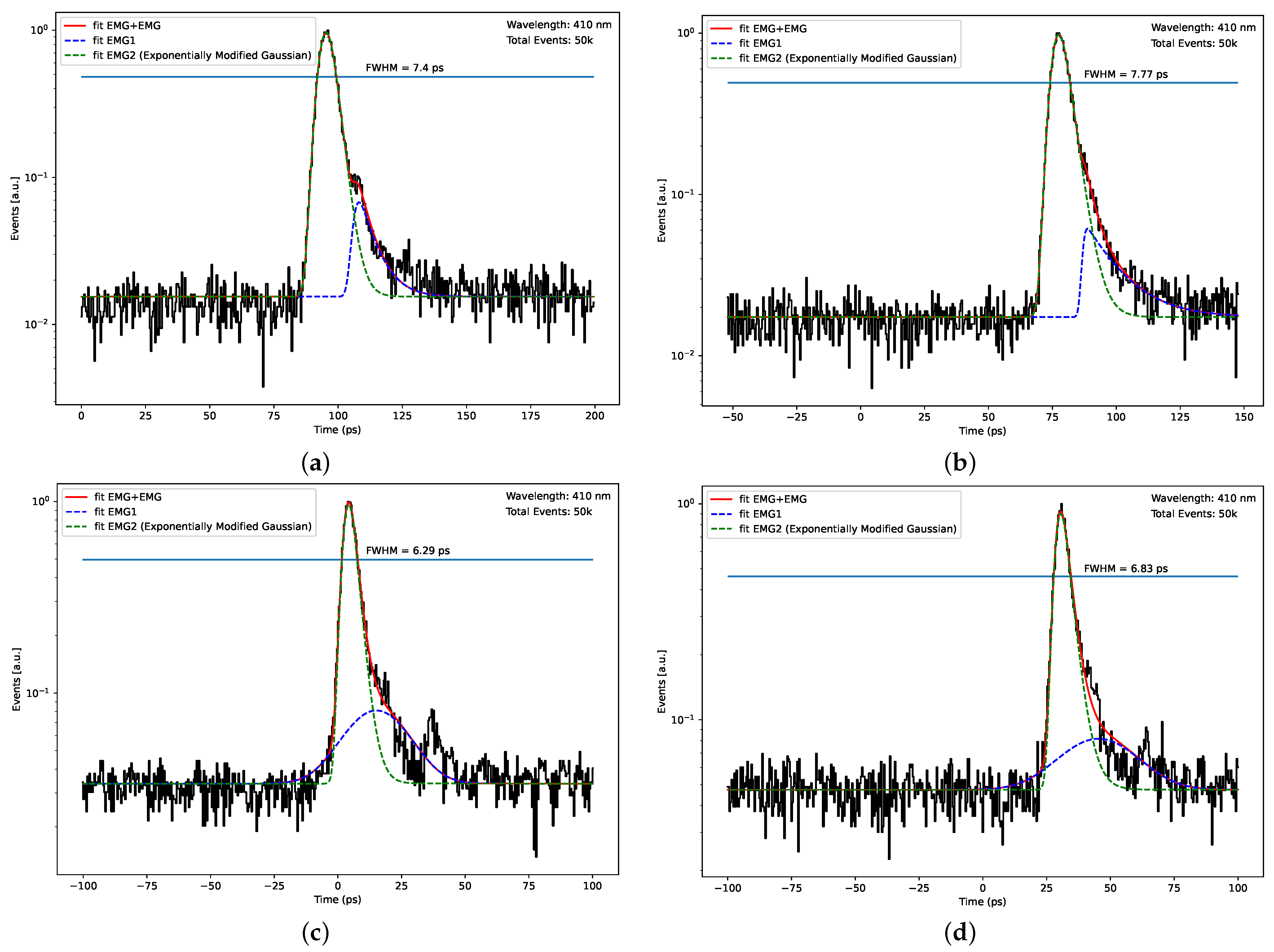
4.4. Single-Photon Timing Resolution
4.5. Cascode Transistor Impact on the SPTR
5. Discussion
6. Conclusions
Author Contributions
Funding
Data Availability Statement
Conflicts of Interest
References
- Lecoq, P. Pushing the Limits in Time-of-Flight PET Imaging. IEEE Trans. Radiat. Plasma Med. Sci. 2017, 1, 473–485. [Google Scholar] [CrossRef]
- Conti, M.; Bendriem, B. The new opportunities for high time resolution clinical TOF PET. Clin. Transl. Imaging 2019, 7, 139–147. [Google Scholar] [CrossRef]
- Rossignol, J.; Turtos, R.M.; Gundacker, S.; Gaudreault, D.; Auffray, E.; Lecoq, P.; Bérubé-Lauzière, Y.; Fontaine, R. Time-of-flight computed tomography—Proof of principle. Phys. Med. Biol. 2020, 65, 085013. [Google Scholar] [CrossRef] [PubMed]
- Lecoq, P.; Morel, C.; Prior, J.O.; Visvikis, D.; Gundacker, S.; Auffray, E.; Križan, P.; Turtos, R.M.; Thers, D.; Charbon, E.; et al. Roadmap toward the 10 ps time-of-flight PET challenge. Phys. Med. Biol. 2020, 65, 21RM01. [Google Scholar] [CrossRef]
- Grim, J.Q.; Christodoulou, S.; Di Stasio, F.; Krahne, R.; Cingolani, R.; Manna, L.; Moreels, I. Continuous-wave biexciton lasing at room temperature using solution-processed quantum wells. Nat. Nanotechnol. 2014, 9, 891–895. [Google Scholar] [CrossRef]
- Gundacker, S.; Martinez Turtos, R.; Kratochwil, N.; Pots, R.H.; Paganoni, M.; Lecoq, P.; Auffray, E. Experimental time resolution limits of modern SiPMs and TOF-PET detectors exploring different scintillators and Cherenkov emission. Phys. Med. Biol. 2020, 65, 025001. [Google Scholar] [CrossRef] [PubMed]
- Tomanová, K.; Čuba, V.; Brik, M.G.; Mihóková, E.; Martinez Turtos, R.; Lecoq, P.; Auffray, E.; Nikl, M. On the structure, synthesis, and characterization of ultrafast blue-emitting CsPbBr3 nanoplatelets. APL Mater. 2019, 7, 011104. [Google Scholar] [CrossRef] [Green Version]
- Loignon-Houle, F.; Gundacker, S.; Toussaint, M.; Lemyre, F.C.; Auffray, E.; Fontaine, R.; Charlebois, S.A.; Lecoq, P.; Lecomte, R. DOI estimation through signal arrival time distribution: A theoretical description including proof of concept measurements. Phys. Med. Biol. 2021, 66, 095015. [Google Scholar] [CrossRef]
- Ito, M.; Hong, S.J.; Lee, J.S. Positron emission tomography (PET) detectors with depth-of- interaction (DOI) capability. Biomed. Eng. Lett. 2011, 1, 70. [Google Scholar] [CrossRef]
- Surti, S. Update on time-of-flight PET imaging. J. Nucl. Med. Off. Publ. Soc. Nucl. Med. 2015, 56, 98–105. [Google Scholar] [CrossRef] [PubMed] [Green Version]
- Vandenberghe, S.; Mikhaylova, E.; D’Hoe, E.; Mollet, P.; Karp, J.S. Recent developments in time-of-flight PET. EJNMMI Phys. 2016, 3, 3. [Google Scholar] [CrossRef] [Green Version]
- van Sluis, J.; de Jong, J.; Schaar, J.; Noordzij, W.; van Snick, P.; Dierckx, R.; Borra, R.; Willemsen, A.; Boellaard, R. Performance Characteristics of the Digital Biograph Vision PET/CT System. J. Nucl. Med. 2019, 60, 1031–1036. [Google Scholar] [CrossRef]
- Gundacker, S.; Turtos, R.M.; Auffray, E.; Paganoni, M.; Lecoq, P. High-frequency SiPM readout advances measured coincidence time resolution limits in TOF-PET. Phys. Med. Biol. 2019, 64, 055012. [Google Scholar] [CrossRef]
- Pratte, J.F.; Nolet, F.; Parent, S.; Vachon, F.; Roy, N.; Rossignol, T.; Deslandes, K.; Dautet, H.; Fontaine, R.; Charlebois, S.A. 3D Photon-To-Digital Converter for Radiation Instrumentation: Motivation and Future Works. Sensors 2021, 21, 598. [Google Scholar] [CrossRef] [PubMed]
- Frach, T.; Prescher, G.; Degenhardt, C.; de Gruyter, R.; Schmitz, A.; Ballizany, R. The digital silicon photomultiplier—Principle of operation and intrinsic detector performance. In Proceedings of the 2009 IEEE Nuclear Science Symposium Conference Record (NSS/MIC), Orlando, FL, USA, 25–31 October 2009. [Google Scholar] [CrossRef]
- Carimatto, A.; Ulku, A.; Lindner, S.; Gros-Daillon, E.; Rae, B.; Pellegrini, S.; Charbon, E. Multipurpose, Fully Integrated 128 × 128 Event-Driven MD-SiPM With 512 16-Bit TDCs With 45-ps LSB and 20-ns Gating in 40-nm CMOS Technology. IEEE Solid-State Circuits Lett. 2018, 1, 241–244. [Google Scholar] [CrossRef]
- Hutchings, S.W.; Johnston, N.; Gyongy, I.; Al Abbas, T.; Dutton, N.A.W.; Tyler, M.; Chan, S.; Leach, J.; Henderson, R.K. A Reconfigurable 3-D-Stacked SPAD Imager With In-Pixel Histogramming for Flash LIDAR or High-Speed Time-of-Flight Imaging. IEEE J. Solid-State Circuits 2019, 54, 2947–2956. [Google Scholar] [CrossRef] [Green Version]
- Nolet, F.; Lemaire, W.; Dubois, F.; Roy, N.; Carrier, S.; Samson, A.; Charlebois, S.A.; Fontaine, R.; Pratte, J.F. A 256 Pixelated SPAD readout ASIC with in-Pixel TDC and embedded digital signal processing for uniformity and skew correction. Nucl. Instrum. Methods Phys. Res. Sect. A Accel. Spectrometers Detect. Assoc. Equip. 2020, 949, 162891. [Google Scholar] [CrossRef]
- Lemaire, W.; Nolet, F.; Dubois, F.; Therrien, A.C.; Pratte, J.F.; Fontaine, R. Embedded time of arrival estimation for digital silicon photomultipliers with in-pixel TDCs. Nucl. Instrum. Methods Phys. Res. Sect. A Accel. Spectrometers Detect. Assoc. Equip. 2020, 959, 163538. [Google Scholar] [CrossRef]
- Nolet, F.; Parent, S.; Roy, N.; Mercier, M.O.; Charlebois, S.A.; Fontaine, R.; Pratte, J.F. Quenching Circuit and SPAD Integrated in CMOS 65 nm with 7.8 ps FWHM Single Photon Timing Resolution. Instruments 2018, 2, 19. [Google Scholar] [CrossRef] [Green Version]
- Nolet, F.; Dubois, F.; Roy, N.; Parent, S.; Lemaire, W.; Massie-Godon, A.; Charlebois, S.A.; Fontaine, R.; Pratte, J.F. Digital SiPM channel integrated in CMOS 65 nm with 17.5 ps FWHM single photon timing resolution. Nucl. Instrum. Methods Phys. Res. Sect. A Accel. Spectrometers Detect. Assoc. Equip. 2018, 912, 29–32. [Google Scholar] [CrossRef]
- Acerbi, F.; Ferri, A.; Gola, A.; Cazzanelli, M.; Pavesi, L.; Zorzi, N.; Piemonte, C. Characterization of Single-Photon Time Resolution: From Single SPAD to Silicon Photomultiplier. IEEE Trans. Nucl. Sci. 2014, 61, 2678–2686. [Google Scholar] [CrossRef]
- Acerbi, F.; Ferri, A.; Gola, A.; Zorzi, N.; Piemonte, C. Analysis of single-photon time resolution of FBK silicon photomultipliers. Nucl. Instrum. Methods Phys. Res. Sect. A Accel. Spectrometers Detect. Assoc. Equip. 2015, 787, 34–37. [Google Scholar] [CrossRef]
- Hsu, M.J.; Finkelstein, H.; Esener, S.C. A CMOS STI-Bound Single-Photon Avalanche Diode With 27-ps Timing Resolution and a Reduced Diffusion Tail. IEEE Electron Device Lett. 2009, 30, 641–643. [Google Scholar] [CrossRef]
- Gramuglia, F.; Wu, M.L.; Bruschini, C.; Lee, M.J.; Charbon, E. A Low-noise CMOS SPAD Pixel with 12.1 ps SPTR and 3 ns Dead Time. IEEE J. Sel. Top. Quantum Electron. 2021, 28, 3800809. [Google Scholar] [CrossRef]
- Rech, I.; Labanca, I.; Armellini, G.; Gulinatti, A.; Ghioni, M.; Cova, S. Operation of silicon single photon avalanche diodes at cryogenic temperature. Rev. Sci. Instrum. 2007, 78, 063105. [Google Scholar] [CrossRef]
- Ghioni, M.; Gulinatti, A.; Rech, I.; Maccagnani, P.; Cova, S. Large-area low-jitter silicon single photon avalanche diodes. Proc. SPIE 2008, 6900, 69001D. [Google Scholar] [CrossRef]
- Gramuglia, F.; Ripiccini, E.; Fenoglio, C.A.; Wu, M.L.; Paolozzi, L.; Bruschini, C.; Charbon, E. Sub-10 ps Minimum Ionizing Particle Detection With Geiger-Mode APDs. Front. Phys. 2022, 10, 370. [Google Scholar] [CrossRef]
- Marwick, M.; Andreou, A. Single photon avalanche photodetector with integrated quenching fabricated in TSMC 0.18 μm 1.8 V CMOS process. Electron. Lett. 2008, 44, 643–644. [Google Scholar] [CrossRef]
- Pratte, J.; Junnarkar, S.; Deptuch, G.; Fried, J.; O’Connor, P.; Radeka, V.; Vaska, P.; Woody, C.; Schlyer, D.; Stoll, S.; et al. The RatCAP Front-End ASIC. IEEE Trans. Nucl. Sci. 2008, 55, 2727–2735. [Google Scholar] [CrossRef]
- Crotti, M.; Rech, I.; Acconcia, G.; Gulinatti, A.; Ghioni, M. A 2-GHz Bandwidth, Integrated Transimpedance Amplifier for Single-Photon Timing Applications. IEEE Trans. Very Large Scale Integr. (VLSI) Syst. 2015, 23, 2819–2828. [Google Scholar] [CrossRef]
- Nemallapudi, M.; Gundacker, S.; Lecoq, P.; Auffray, E. Single photon time resolution of state of the art SiPMs. J. Instrum. 2016, 11, P10016. [Google Scholar] [CrossRef]
- Sanzaro, M.; Gattari, P.; Villa, F.; Tosi, A.; Croce, G.; Zappa, F. Single-Photon Avalanche Diodes in a 0.16 μm BCD Technology With Sharp Timing Response and Red-Enhanced Sensitivity. IEEE J. Sel. Top. Quantum Electron. 2018, 24, 3801209. [Google Scholar] [CrossRef] [Green Version]
- Dalla Mora, A.; Tosi, A.; Tisa, S.; Zappa, F. Single-Photon Avalanche Diode Model for Circuit Simulations. IEEE Photonics Technol. Lett. 2007, 19, 1922–1924. [Google Scholar] [CrossRef]
- Giustolisi, G.; Mita, R.; Palumbo, G. Verilog-A modeling of SPAD statistical phenomena. In Proceedings of the 2011 IEEE International Symposium of Circuits and Systems (ISCAS), Rio de Janeiro, Brazil, 15–18 May 2011. [Google Scholar] [CrossRef]
- Gramuglia, F. High-Performance CMOS SPAD-Based Sensors for Time-of-Flight PET Applications. Ph.D. Thesis, EPFL, Lausanne, Switzerland, 2022; p. 247. [Google Scholar] [CrossRef]
- Charbon, E.; Hyyung-June, Y.; Maruyama, Y. A Geiger mode APD fabricated in standard 65 nm CMOS technology. In Proceedings of the 2013 IEEE International Electron Devices Meeting (IEDM), Washington, DC, USA, 9–11 December 2013; Volume 27, pp. 1–4. [Google Scholar] [CrossRef]
- Webster, E.A.G.; Richardson, J.A.; Grant, L.A.; Renshaw, D.; Henderson, R.K. A Single-Photon Avalanche Diode in 90-nm CMOS Imaging Technology With 44% Photon Detection Efficiency at 690 nm. IEEE Electron Device Lett. 2012, 33, 694–696. [Google Scholar] [CrossRef]
- Xu, H.; Pancheri, L.; Betta, G.F.D.; Stoppa, D. Design and characterization of a p+/n-well SPAD array in 150 nm CMOS process. Opt. Express 2017, 25, 12765–12778. [Google Scholar] [CrossRef] [PubMed]
- Korzh, B.; Zhao, Q.Y.; Allmaras, J.P.; Frasca, S.; Autry, T.M.; Bersin, E.A.; Beyer, A.D.; Briggs, R.M.; Bumble, B.; Colangelo, M.; et al. Demonstration of sub-3 ps temporal resolution with a superconducting nanowire single-photon detector. Nat. Photonics 2020, 14, 250–255. [Google Scholar] [CrossRef] [Green Version]
- Keysight Technologies—Infiniium 90000 X-Series Oscilloscopes. Available online: https://www.keysight.com/us/en/assets/7018-02436/data-sheets/5990-5271.pdf (accessed on 1 October 2022).


| Cascoded | Cascoded | Cascoded | Unbalanced | Standard | ||
|---|---|---|---|---|---|---|
| Characteristics | Comp. | Unbalanced | Standard | Comp. | 3.3 V Inv. | 3.3 V Inv. |
| 1 V Inv. | 1 V Inv. | |||||
| Figure 1 circuits | A & D | C & E | E | E | B & D | D |
| Discriminator size (µm2) | 104 | 24 | 6 | 104 | 88 | 40 |
| Cascode size (µm2) | 63 | 63 | 63 | |||
| Discriminator and | 104 | 87 | 69 | 167 | 88 | 40 |
| cascode size (µm2) | ||||||
| Inverter NMOS W/L ratio | 40 | 2 | 48 | 8 | ||
| Inverter PMOS W/L ratio | 4 | 2 | 2.5 | 2.5 | ||
| Maximum excess voltage | 3.3 | 4.3 | 4.3 | 6.6 | 3.3 | 3.3 |
| QC Jitter (ps FWHM) | 4 | 2 | 3 | 4 | 2 | 3 |
| Characteristics | This Work | [36] | [20] | [37] | [38] | [39] | [33] | [24] | [28] |
|---|---|---|---|---|---|---|---|---|---|
| Technology (nm) | 65 | 55 | 65 | 65 | 90 | 150 | 160 | 180 | 180 |
| / (V) | 9.9/1.7 | 31/7 | 9.9/1.5 | 9/0.4 | 15/2.4 | 18/3 | 26/3–9 | 11/0.8 | 22/8 |
| Diameter (µm) | 17.6 | 8.8 | 20 | 8 | 6.4 | 10 | 10–80 | 14 | 25 |
| DCR (cps/µm) | 0.6 k | 2.6 | 2.8 k | 15.6 k | 3.1 | 0.4 | 0.13 | 4 k | 0.2 |
| Afterpulsing (%) | <1 | <1 | <10 | <1 | 0.85 | <1 | <1.26 | N/A | <0.1 |
| @ Hold-off | 0.1 µs | 4.5 ns | 0.1 µs | 5 µs | 15 ns | 150 ns | 50 ns | N/A | 3 ns |
| Peak PDE (%) | 27 | 62 | 8 | 5.5 | 44 | 31 | 71 | N/A | 55 |
| SPTR (ps FWHM) | 6.3 | 30 | 7.8 | 235 | 51 | 42 | 28 | 27 | 7.5 |
| Discriminator | Simulation | Measurements | ||||
|---|---|---|---|---|---|---|
| Min | Typ. | Max | Min | Median | Max | |
| Comparator | 6.5 | 7.3 | 8.7 | 7.0 | 7.4 | 7.8 |
| Inverter 1 V UB | 6.6 | 7.1 | 8.3 | 7.5 | 7.7 | 8.4 |
| Inverter 1 V Std | 6.9 | 7.6 | 9.0 | 8.1 | 8.9 | 9.4 |
| Inverter 3.3 V UB | 7.2 | 9.1 | 12.0 | 8.5 | 9.2 | 10.1 |
| Inverter 3.3 V Std | 9.2 | 11.3 | 14.2 | 9.5 | 10.1 | 10.8 |
| Characteristics | Cascoded | Cascoded | Cascoded | UB | Std | |
|---|---|---|---|---|---|---|
| Comp. | UB 1 V Inv. | Std 1 V Inv. | Comp. | 3.3 V Inv. | 3.3 V Inv. | |
| Total discriminator | 104 | 87 | 69 | 167 | 88 | 40 |
| size (µm2) | ||||||
| Maximum excess voltage (V) | 3.3 | 4.3 | 4.3 | 6.6 | 3.3 | 3.3 |
| QC jitter (ps FWHM) | 4 | 2 | 3 | 4 | 2 | 3 |
| Static power | 165 | 0 | 0 | 165 | 0 | 0 |
| consumption (µW) | ||||||
| Best SPTR (ps FWHM) | 6.3 | 6.8 | 8.1 | 7.0 | 8.4 | 9.5 |
| at 1.7 excess voltage | ||||||
| Best SPTR (ps FW(1/10)M) | 14.31 | 17.9 | 18.8 | 16.2 | 25.8 | 30.2 |
| at 1.7 excess voltage | ||||||
| Best SPTR (ps FW(1/100)M) | 32.4 | 36.6 | 36.14 | 44.2 | 45.6 | 49.1 |
| at 1.7 excess voltage |
Disclaimer/Publisher’s Note: The statements, opinions and data contained in all publications are solely those of the individual author(s) and contributor(s) and not of MDPI and/or the editor(s). MDPI and/or the editor(s) disclaim responsibility for any injury to people or property resulting from any ideas, methods, instructions or products referred to in the content. |
© 2023 by the authors. Licensee MDPI, Basel, Switzerland. This article is an open access article distributed under the terms and conditions of the Creative Commons Attribution (CC BY) license (https://creativecommons.org/licenses/by/4.0/).
Share and Cite
Nolet, F.; Gauthier, V.; Parent, S.; Vachon, F.; Roy, N.; St-Jean, N.; Charlebois, S.A.; Pratte, J.-F. Quenching Circuit Discriminator Architecture Impact on a Sub-10 ps FWHM Single-Photon Timing Resolution SPAD. Instruments 2023, 7, 16. https://doi.org/10.3390/instruments7020016
Nolet F, Gauthier V, Parent S, Vachon F, Roy N, St-Jean N, Charlebois SA, Pratte J-F. Quenching Circuit Discriminator Architecture Impact on a Sub-10 ps FWHM Single-Photon Timing Resolution SPAD. Instruments. 2023; 7(2):16. https://doi.org/10.3390/instruments7020016
Chicago/Turabian StyleNolet, Frédéric, Valérie Gauthier, Samuel Parent, Frédéric Vachon, Nicolas Roy, Nicolas St-Jean, Serge A. Charlebois, and Jean-François Pratte. 2023. "Quenching Circuit Discriminator Architecture Impact on a Sub-10 ps FWHM Single-Photon Timing Resolution SPAD" Instruments 7, no. 2: 16. https://doi.org/10.3390/instruments7020016