Article

A Beam Monitor for Ion Beam Therapy Based on HV-CMOS Pixel Detectors

1
Institute for Data Processing and Electronics (IPE), Karlsruhe Institute of Technology, 76131 Karlsruhe, Germany
2
Institute of Experimental Particle Physics (ETP), Karlsruhe Institute of Technology, 76131 Karlsruhe, Germany
3
Heidelberg Ion-Beam Therapy Center (HIT), Department of Radiation Oncology, Heidelberg University Hospital, 69120 Heidelberg, Germany
4
National Center for Tumor Diseases (NCT) and Heidelberg Institute of Radiation Oncology (HIRO), National Center for Radiation Research in Oncology (NCRO), Heidelberg University Hospital, 69120 Heidelberg, Germany
5
Clinical Cooperation Unit Radiation Oncology, German Cancer Research Center (DKFZ) Heidelberg, 69120 Heidelberg, Germany
6
Department of Radiation Oncology and Heidelberg Institute of Radiation Oncology (HIRO), National Center for Radiation Research in Oncology (NCRO), Heidelberg University Hospital, 69120 Heidelberg, Germany
7
Division of Medical Physics in Radiation Oncology and Heidelberg Institute of Radiation Oncology (HIRO), National Center for Radiation Research in Oncology (NCRO), German Cancer Research Center (DZFZ) Heidelberg, 69120 Heidelberg, Germany
*
Author to whom correspondence should be addressed.
Now with Bosch AG, 72762 Reutlingen, Germany.
Instruments 2023, 7(1), 9; https://doi.org/10.3390/instruments7010009
Submission received: 31 October 2022 / Revised: 13 January 2023 / Accepted: 2 February 2023 / Published: 9 February 2023
(This article belongs to the Special Issue Medical Applications of Particle Physics)

Abstract

:
Particle therapy is a well established clinical treatment of tumors. More than one hundred particle therapy centers are in operation world-wide. The advantage of using hadrons like protons or carbon ions as particles for tumor irradiation is the distinct peak in the depth-dependent energy deposition, which can be exploited to accurately deposit doses in the tumor cells. To guarantee this, high accuracy in monitoring and control of the particle beam is of the utmost importance. Before the particle beam enters the patient, it traverses a monitoring system which has to give fast feedback to the beam control system on position and dose rate of the beam while minimally interacting with the beam. The multi-wire chambers mostly used as beam position monitors have their limitations when a fast response time is required (drift time). Future developments such as MRI-guided ion beam therapy pose additional challenges for the beam monitoring system, such as tolerance of magnetic fields and acoustic noise (vibrations). Solid-state detectors promise to overcome these limitations and the higher resolution they offer can create additional benefits. This article presents the evaluation of an HV-CMOS detector for beam monitoring, provides results from feasibility studies in a therapeutic beam, and summarizes the concepts towards the final large-scale assembly and readout system.

1. Introduction

In this section, the concept of ion beam therapy is introduced, followed by the requirements for a beam monitoring system and a description of a state-of-the-art system. This information is based on the beam application and monitoring system of the Heidelberg Ion Beam Therapy center (HIT), but applies to similar ion beam therapy facilities, too. A short review of alternative beam monitoring concepts and devices follows. The section concludes with a description of the newly proposed system.

1.1. Ion Beam Therapy

Today, ion beam therapy as a treatment against cancer is well established after a long history of developments [1]. More than one hundred particle therapy facilities are in operation today (https://www.ptcog.ch/index.php/facilities-in-operation-restricted, accessed on 1 February 2023). Protons or heavier ions can be controlled well, both in energy by the accelerator and in direction by magnetic deflection in the beam delivery system. The sharply peaking dose-versus-depth characteristic (Bragg peak) of these hadrons in tissue, as sketched in Figure 1, allows controlling the depth of the deposited dose in the patient through the energy of the particles.
Using a treatment plan with different raster points in different iso-energy slices (IES), highly conformal irradiation is possible, which maximizes the damage to the tumor while sparing healthy tissue.
HIT came into clinical operation in 2009 [3]. It consists of a chain of ion accelerators designed for the scanning treatment technique which enables three-dimensional control of particle fluence and hence also dose. The technique used here is called fluence-controlled continuous spot scanning [4] and uses a continuously extracted beam while scanning. The lateral motion is stopped at predefined spots until a predefined number of ions has been delivered, before the beam quickly moves to the next spot. Ions are extracted from one of the three ion sources, then accelerated in a linear accelerator (linac) up to 7  M e V /u and injected into the compact synchrotron with a circumference of about 65  m after stripping off all electrons. The ions can reach energies of up to 430  M e V /u. The extracted energy is controlled directly by the synchrotron and may be varied from spill to spill to achieve depth variation. Clinically, carbon ions and protons are used.
Table 1 provides some basic beam parameters.
The ions are guided through the beam transport line to four irradiation rooms. Two horizontal irradiation rooms and one room with a 360° rotating ion gantry are available for patient treatment [5]. A fourth room is used for quality assurance and research activities (QA room), and the measurements with a particle beam presented in Section 4 were performed there. All rooms are equipped for 3D scanning irradiations. The accelerator control system can currently provide 255 different energy settings, 15 intensity steps and 6 spot sizes for each ion species; for practical reasons only a subset of the intensity steps and spot sizes is used. The beam is produced in spills with lengths of up to 5  s and intensities up to 3.2 × 10⁹ s−1 for protons. As the extracted beam intensity is not constant and may vary considerably during extraction, the monitor system is used to measure the number of delivered ions at any time. The beam intensity is controlled dynamically using a feedback loop which involves a monitor chamber [6]. A measurement of the number of particles within a spill performed with an ionization chamber is shown in Figure 2.
When a predefined number of ions is reached, the feedback loop to the scanner magnets triggers the movement of the beam to the next raster point [4]. The spills can be aborted as soon as all raster points in one IES have been irradiated and before the energy has to be switched. Fluence-controlled continuous spot scanning requires a fast (typically within 10  μ s ) monitoring and control feedback loop, which is part of the Beam Application and Monitoring System described in Section 1.2.
To fully benefit clinically from high precision dose delivery by scanned ion beams, image guidance in treatment position during the course of the treatment is mandatory. Real-time imaging can help to locate the target volume in moving tissue and adapting the treatment plan during irradiation, but is currently not available for ion beams. Unlike X-ray based computed tomography (CT), magnetic-resonance imaging (MRI) offers superior soft tissue contrasts and good discrimination between tumors and normal tissue. Moreover, it is not based on ionizing radiation and does not lead to additional imaging doses, which makes it suitable for continuous monitoring. MR-based image guidance for ion beam therapy is technologically even more challenging than photon-based radiotherapy, and its development is still in a very early phase. Recently, studies on the realization of MRI-guided proton therapy have started, with several challenges ahead [7]. Within the ARTEMIS (Adaptive RadioThErapie Mit IonenStrahlen, funded by BMBF) project in Heidelberg, a demonstrator system for implementing MRI-guided ion beam delivery, including online MR imaging of the target region during irradiation, is under development. Specifically, beam control and beam monitoring in the presence of an active MRI device need to cope with magnetic fields and acoustic noise, which specifically poses a problem for multi-wire chambers (MWC) with thin windows (vibrations), and may thus call for alternative detector technologies.

1.2. Beam Monitoring

The beam monitoring system needs to provide information about the position and particle number at each raster point and is placed close to the patient. Additionally, control of the beam spot size is desirable, although this is not actively controlled during beam delivery. The requirements for a next-generation beam monitoring system at HIT can be formulated as follows:
  • Position measurement: The beam position can be calculated as the center of gravity of the induced signals. The accuracy of the calculated position shall be better than 200  μ m .
  • Spot size measurement: The accuracy of the calculated beam spot width shall be better than 10% for a Gaussian shape.
  • Fluence measurement: The number of particles needs to be counted for each raster point. The particle numbers (>10,000 carbon ions; >200,000 protons) shall be measured with 0.5% accuracy.
  • Timing and latency: The position and spot size shall be measured within 100  μ s and delivered to the fast control interface within 100  μ s latency. An updated value shall be delivered to the fast interface every 1 μs to 2  μ s for the fluence measurement and every 50 μs to 100  μ s for the position and width measurement.
  • Radiation tolerance: The system shall be operable for at least five years. For the central position, where the maximum accumulated dose is expected (few mm 2 ), this corresponds to a particle fluence of 3 × 1014 cm−2 with carbon ions and 3 × 1015 cm−2 with protons, which falls off very fast with increasing radial distance. This very localized radiation damage might be an additional challenge for the detector. The radiation damage deteriorates the performance of the system, which needs to be replaced regularly. The regular replacement and recommissioning after five years of operation shall not take longer than one day. More frequent replacements shall not last longer than two hours.
  • Size of sensitive area: The overall active area shall be 25 cm × 25  c m to cover a treatment area of 20 cm × 20  c m including penumbra.
  • Dimensions: The thickness of the outer housing shall be smaller than 5  c m and fit in a cylinder of 60  c m diameter. The material shall correspond to a water-equivalent thickness of less than 0.35 mm.
  • Environment: The detector must tolerate light, acoustic noise and magnetic fields of at least 100  m T in the fringe field of an MRI system (magnetic fields in the iso-center can reach up to 1.5  T ).
The current beam monitoring system at HIT consists of two MWCs (see e.g., [8]) each with one plane for x- and y-direction to measure position and spot size, and three ionization chambers (IC) to track the applied dose. The MWC have a channel pitch of 2  m m , but only a projection of the beam spot can be measured. The signal from the first MWC is used to control a feedback loop for the beam position; the position is monitored by the second MWC. If the deviation between both measurements of position and width exceeds a threshold, a beam interlock is triggered. Both chambers are also used to derive a spot size measurement, on which an interlock is defined, in case upper and lower thresholds are exceeded. The integrated signal from the first IC controls the progress of the irradiation, and the beam is moved to the next raster point when the desired dose is reached. The other two ICs serve as independent checks of the particle fluence and ensure redundancy and diversity. If the deviation between the ICs exceeds a threshold, a beam interlock is triggered.
The MWCs have some limitations, apart from their resolution, which restrict their field of application. The concept of gas ionization and drift of charge carriers is limited to the drift velocity of the ions in gas. The signal is slightly delayed with respect to the first particles traversing the detector and there is still ion drift left when the particles have disappeared. These delays can be up to several hundreds of microseconds [9], which delays the interlocks, so that several raster points may be affected, before abort. The performance of MWCs can also be affected by acoustic noise which can lead to vibrations of the wires and therefore deterioration of the resolution. One possible source of such acoustic noise can be an MRI system used for online position control of the target. At the HIT QA room, an MRI system (Section 3.2) for developing MRI-guided ion beam therapy is available for testing the behavior of novel beam monitors.

1.3. Alternative Beam Monitoring Concepts and Devices

For more than 10 years, the research community has been searching for improved detectors for high-rate beam monitoring. This section is not intended to be complete, but rather to give a short introduction to some recent attempts. An extensive review is given, for example, in [10].
Some approaches are gas-based, such as the Time Projection Chamber-like approach described in [11], the improved segmented ionization strip chambers with a spatial resolution of 100  μ m in [12], or a more vibration tolerant version of an ionization chamber in [9]. They all have in common that the charge collection time is in the order of milliseconds and that very fast feedback on the timescale of few hundred microseconds is not possible.
One different approach is the measurement of the magnetic field of the deflecting magnets in the beam delivery system. The field strength is proportional to the final position of the beam spot and provides very fast (10  μ s ) and precise (10  μ m ) beam position measurement [13]. One drawback might be that the measurement is performed at quite a distance (more than about 5  m ) from the patient and so the beam could be deflected by other sources, e.g., the magnetic field of an MRI, in its path. In addition, remanence effects and dependencies on the beam position in the beam line can deteriorate the projected beam position at the target.
Scintillating fibers coupled to silicon photomultipliers (SiPM) are already used as fast, large area beam monitors [14,15,16]. The drawback here is the weak radiation tolerance, which is limited to 1000 patient treatments for the device as discussed in [16]. Additionally, a reduction of the attenuation length below 10% after a dose of about 50  kGy is indicated in [17]. Using photo diodes to read out scintillating fibers is investigated in [18]. There, it is also suggested that fibers with higher radiation hardness be used, not only as a natural attempt to overcome this weakness but also to profit from the shift in the emitted light spectrum.
An interesting attempt based on silicon is documented in [19]. The investigated large-scale detector (20 cm × 20  c m ) is a commercial amorphous silicon based X-ray imager, but in this case applied to an ion beam. The resolution and stability over a period of 4 h was very good, but the readout time was still high (80  m s /frame). The radiation tolerance over a period of one year needs to be evaluated.
Another promising silicon detector type is that of Ultra Fast Silicon Detectors (UFSD) based on thin Low Gain Avalanche Detectors (LGAD). Three examples of applying this detector type in particle therapy applications can be found in [20,21,22]. These detectors can be used for very fast timing applications like time-of-flight detector systems. The good time resolution of better than 100 ps is a result of the intrinsic signal gain of these devices, which is about 10 to 20. This gain (and the time resolution) is reduced significantly after irradiation. A gain reduction of 20% after a fluence of 1 × 1012 cm−2 is quoted in [20]. This is small compared to the yearly expected fluence in the center of a beam monitoring detector. This detector type requires external readout electronics. For a pixellated layout, the readout electronics need to be connected via bump bonds to the LGAD, adding material and complexity during assembly.
To avoid the interconnection step, reduce material and bring the first signal amplification stage close to the generated signal, monolithic detector chips have been developed. In [23], a commercial large-scale CMOS detector for X-ray imaging was evaluated as a proton beam monitor. The determination of the beam profile was shown to reproduce measurements with films with minor deviations as long as saturation was not reached. The rolling shutter readout mode of this device limits the readout speed and a full readout of the 12 cm × 14  c m -large matrix leads to saturation effects already at low beam currents. For this device, no evaluation of the radiation tolerance was reported in [23].

1.4. A Beam Monitor Based on HV-CMOS Detectors

In this article, a novel approach is discussed based on custom HV-CMOS detectors, introduced in Section 2. These monolithic devices combine the sensing element with signal processing in one thin silicon chip. For fast readout, the chips implement particle counting and projection of particle counts on the x- and y-axis. The reticle-sized chips will be arranged in a 13 × 13 array to achieve the required active area of 25 cm × 25  c m and interconnected by thin flex PCBs to the surrounding electronics, where electrical signals are converted to optical signals which allow stable data transmission to a fast field-programmable gate array (FPGA) board for further data processing. The chip array is mounted on thin carbon fiber plates for mechanical and thermally dissipative support. Figure 3 shows a schematic 3D rendering of the final detector design.
After the introduction of the chip technology in Section 2, the systems and facilities used for the characterizing measurements are described in Section 3 and, finally, the evaluation of the detector and system performance is discussed in Section 4.

2. A Beam Monitoring Chip Based on HV-CMOS Technology

2.1. Silicon Sensor Technology

Particle detectors made of silicon base material are widely used in experimental particle physics [24] and have been proposed for usage in radiotherapy for many years [25]. They are operated in high magnetic fields (up to 3.8  T ) and high particle fluxes (up to 3.5 GHz cm−2). The basic building blocks are pn-junctions operated in reverse bias. Traversing charged particles generate electron-hole pairs by ionization (about 75 per μ m ) in the depleted silicon bulk, and the readout electronics detect the produced current pulses. For hybrid systems, the readout electronics are implemented on dedicated ASICs which are connected to the silicon sensor by wire bonds in case of planar strip sensors or bump bonds for pixelated sensors [26,27]. The hybrid approach allows combining a specialized sensor with specialized readout electronics, which are developed independently. Still, the hybridization requires additional and potentially expensive production steps. It also limits the granularity and mass (saving) of the final detector. An alternative consists of monolithic devices, described in the next section.

2.2. The HV-CMOS Technology

CMOS technology allows combining the sensitive pn-junction with the readout electronics on one thin (less than 150  μ m ) chip. While keeping the high granularity of a pixel sensor, this approach avoids the additional readout chip (reducing material thickness) and the connectivity step (reducing costs). The radiation environment in experimental particle physics and beam monitoring calls for silicon chips with increased radiation tolerance. One possibility is to use a commercially available High-Voltage CMOS (HV-CMOS) process [28]. This technology allows applying a bias voltage of up to about 300  V , generating a wide depletion zone (typically 35 μm to 50  μ m ). Generated charge carriers are then collected by fast drift (in the order of few ns) in the electric field, and not only by slow diffusion as in standard CMOS devices. The faster drift reduces the effect of charge carrier trapping [29] in irradiated silicon and more charge carriers are generated in the wider depletion zone, yielding a higher signal. At least the electronics of the first steps of signal processing are located inside the pixels (smart diode). Typically, signal amplification and digitization circuits are also added. Combining improved radiation tolerance with integrated electronics and small pixel sizes makes the HV-CMOS technology a promising candidate for a beam monitoring system. Several HV-CMOS-based detectors have been developed for particle physics experiments so far [30,31,32,33].

2.3. An HV-CMOS Detector for Beam Monitoring

The beam monitoring detector chip HitPix has been developed in 180  n m HV-CMOS technology and was produced in two generations. HitPix1 has 24 × 24 pixels, is 5 mm × 5 mm in size and is described in detail in [34,35]. HitPix2 has 48 × 48 pixels, is 10 mm × 10 mm in size and is the generation investigated in this article. The chip was designed as part of a PhD thesis [35] and evaluated in [36]. The dimensions of a detector chip for the envisaged final beam monitoring system will be 20 mm × 20 mm with 96 × 96 pixels. In this section, only the main features of the HitPix family in view of the targeted application are summarized.
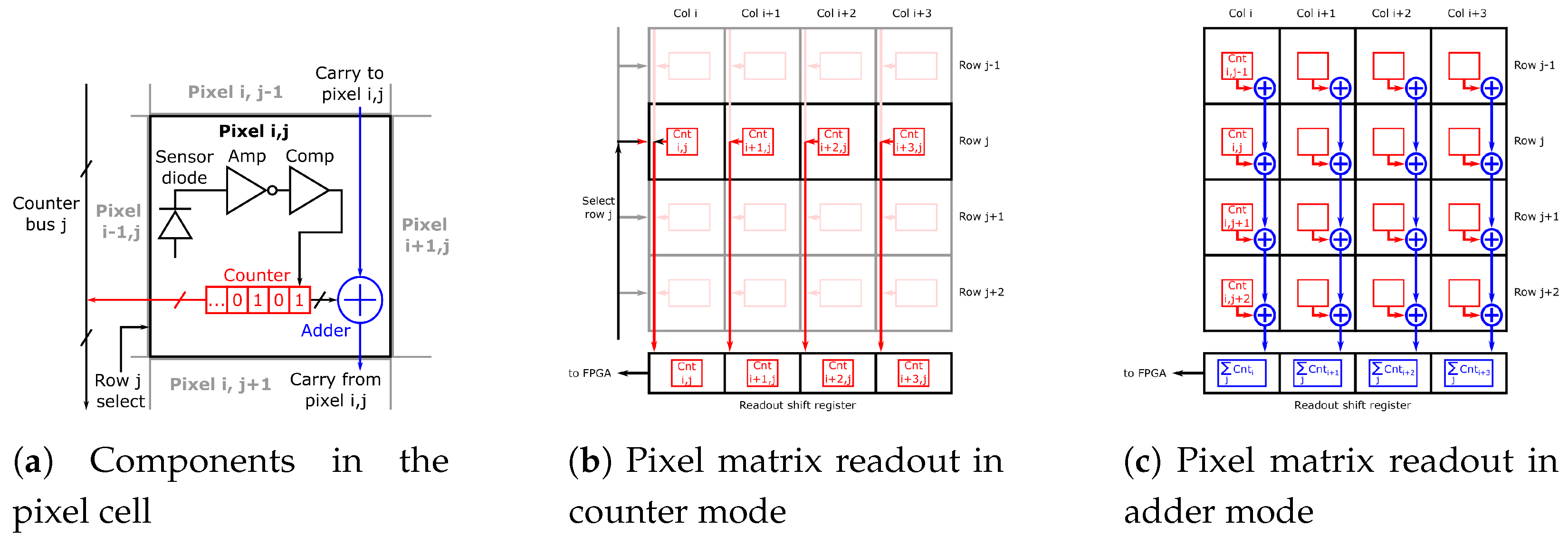
The very high particle rates can be processed by counting the particle transitions in each pixel cell during a programmable period of several microseconds. One hit is registered when the induced signal of a charged particle traversing a pixel cell passes a programmable threshold, which needs to be optimized with respect to noise and induced signal. The hit counts are accumulated over a programmable time period. The resulting count status of the pixel matrix is called a frame. One frame can then be read out, either for each pixel of the matrix (counter readout, slow) or for the sums of each row and column (adder readout, fast), which are calculated on-chip. In the counter readout mode the readout takes longer since more data (129,024 bits per frame for the final chip) are handled. It is used for debugging or detailed beam diagnostics, since some skewed beam shapes can only be detected with two-dimensional measurements. In the adder readout mode, the projected data (2688 bits per frame for the final chip) can be read out 48 times faster, while the pixel hit counting continues. The adding step happens quasi instantaneously when any counter in the corresponding row/column is increased, and all sums are transferred to the shift register by one load pulse when the readout is triggered (this introduces about 1.4 μs of dead time for the current test system).
The concept is illustrated in Figure 4.
It is clear that the projections in adder readout mode do not contain the full information on the beam shape, but the most relevant, such as position and width. The shape is typically constant on the scale of an irradiation day, and therefore the projections of the beam profile are sufficient to generate a fast interlock in case the beam behaves unexpectedly.
The required pixel size was evaluated from cluster size measurements with available HV-CMOS detectors featuring a similar charge collecting diode structure, but smaller pixels, and the requirement to reach at least 200  μ m position resolution. The ionization of therapeutic ions is much larger than minimum ionizing particles as they typically appear in particle physics experiments. Protons in the range given in Table 1 generate 2 to 6 times more charge and carbon ions 50 to 135 times more. Although the deposited charge is much higher, the average cluster size was measured to be below two pixels for 150 μm × 50  μ m pixels for these type of ions [37]. This means that the charge of one particle can be well contained in a 200 μm × 200  μ m pixel, also fulfilling the requirement for a resolution of at least 200  μ m .
Another aspect for the chip design is a narrow inactive periphery, which was achieved by locating data processing (analog-to-digital converters, hit counters, hit adders) and data storage inside each pixel. The periphery houses only configuration storage and a simple shift register readout.
The HitPix2 is prepared for daisy-chain readout of several detectors to minimize readout lines on the interconnecting cable when moving to a multi-chip array. The chain can be up to seven detectors long. For the final system, the detectors will have 96 × 96 pixels and two projections with 14 bits per line. This results in 18,816 bits for a chain containing seven detectors to be read out in adder mode during the integration time of one frame, which is in the order of 20  μ s depending on the beam intensity. To achieve this, a data rate of about 1 GHz is required. In case the readout time for many detectors in a daisy-chain turns out to not meet the specifications, each detector has an additional direct readout option. In this mode, the selection of individual detectors for readout is possible to define a region-of-interest for each frame and, to save data traces on the flex cable, allows using a common data bus structure sharing the signals of some detectors on one line.

3. Irradiation Facility and Test Environments

3.1. Irradiation facility

To accumulate a significant particle fluence in short time, a compact cyclotron with 23  M e V protons was used. The cyclotron is operated by the company ZAG Zyklotron AG (ZAG, https://www.zyklotron-ag.de/index.php, accessed on 1 February 2023) and is situated on the Campus North of KIT. The beam has a width of about 8  m m (FWHM) and the beam current is set to about 2  μ A for irradiation of the detectors. At this beam current, the samples are irradiated to the target fluence of around 1 × 1015 cm−2 within 15  min . The samples are placed inside an insulated box which is flushed with cold nitrogen gas (below −20 °C). The box is scanned in front of the beam to achieve uniform irradiation of the samples. The damage to the silicon lattice caused by these protons can be converted into an equivalent damage caused by 1  M e V neutrons with the non-ionization energy loss (NIEL) hypothesis [38]. The particle fluence F particle can be converted to the equivalent fluence as F eq = κ × F particle . The corresponding scaling factor is called hardness factor κ , with  κ = 2.0 for 23  M e V protons.

3.2. Magnetic Field Test Environments

The HV-CMOS technology does not only have the potential to improve the performance of the existing beam monitoring system, but the tolerance of silicon sensors towards magnetic fields promises the simultaneous irradiation and MR imaging of the target. While most sensor technologies can be operated at a certain distance from the high field region of an MRI system, HV-CMOS sensors are expected to work within the center of the field. HIT has built a large scale Helmholtz coil pair with an inner diameter of 60  c m for measurements in a magnetic field of up to 100  m T under lab conditions. A picture of the setup is shown in Figure 5a. It was used for basic measurements in a static field with the HV-CMOS detectors.
In order to measure the effect on the detector of the even stronger field of an MRI magnet and its alternating field during scanning, an MRI system (Esaote S-Scan) was used which is available in the QA room at HIT, with a static magnetic field of 250  m T . The MRI system is located inside an enclosure for shielding the stray fields as shown in Figure 5b. The whole setup can be moved into the beam for experiments. It was used for the tests reported in Section 4.6.

3.3. Data Acquisition System

The test system for control and read out of the detectors is split into four parts.
The detectors are mounted and wire-bonded on a simple PCB called carrier. The carrier can be plugged into a PCIe socket of the GEneric Configuration and COntrol board (GECCO) [37,39]. GECCO provides all necessary supply voltages as well as test signals and routes data lines from and to an FPGA. In this case, a Nexys Video Artix-7 FPGA board (https://digilent.com/shop/nexys-video-artix-7-fpga-trainer-board-for-multimedia-applications/, accessed on 1 February 2023) is used.
The firmware for controlling the detector implements a state machine. Communication to the HitPix detector is established via a two-phase shift register driven by the FPGA with up to 200 Mbit s−1.
Finally, the hardware is connected to a PC by USB. The software interacting with the FPGA uses multi-threading to receive and decode data from the FPGA as quickly as possible while online data processing can continue.
Figure 6 shows a block diagram of the data acquisition chain with the different elements and the data streams.

3.4. Simulation Environment

Since the proposed beam monitoring system marks a transition from gas-filled chambers to solid state detectors, the material effect on the beam needs to be studied. For this, a simulation with the GEANT4 toolkit [40] was performed comparing the current system at HIT with the proposed system described in Section 1.4. The setup of the simulation is illustrated in Figure 7.
The narrow blue layer represents the three ICs with a water-equivalent thickness of 3   × 230  μ m  [41]. This corresponds to the scenario in which the HitPix system only replaces the MWCs for beam position and shape monitoring. In another scenario, the HitPix system could even replace the ICs if the dose measurement is proven to be compatible. This would reduce the material budget further. The green layers in Figure 7 represents either the MWCs (160  μ m water equivalent [41]) or the HitPix system. The HitPix system consists of 200  μ m carbon-fiber-reinforced polymer as the thermal and mechanical support, 100  μ m of silicon for the thinned detectors and 90  μ m polyimide as a flex cable with 7  μ m of either aluminum or copper per side. An area factor is applied for the metal traces to account for 80  μ m wide traces at 200  μ m pitch. For comparison, carbon ions at 128.1  M e V /u were used as primary beam, traversing the beam monitoring arrangement and entering a water target after about 1.2  m in air.

4. Detector Characterization and Evaluation as a Beam Monitoring Device

This section summarizes the characterization of the detector technology and describes the evaluation studies in view of the beam monitoring application performed so far.

4.1. Technology Decisions

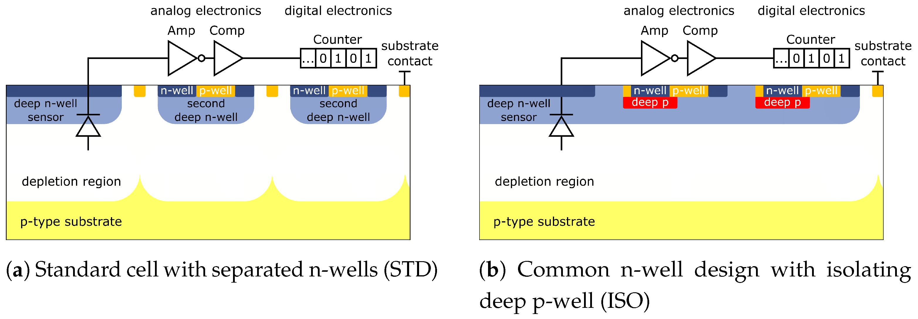
Since the beam monitoring detector should register nearly all traversing particles, the insensitive regions need to be very small. Therefore, the insensitive periphery of the detector can only occupy a small fraction of the overall detector area. This is possible by using simple and area-saving building blocks for the communication part and moving data processing blocks into the pixel cells.
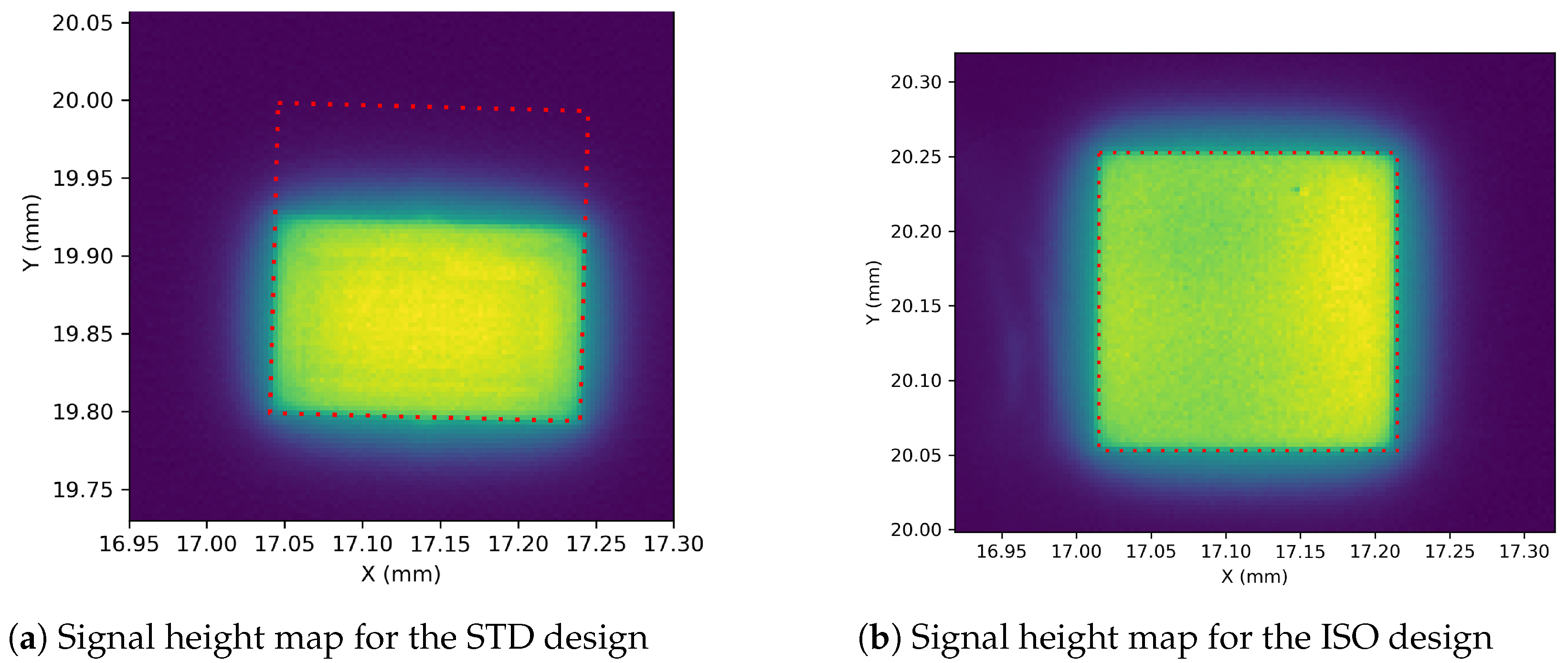
The first version of HitPix was produced in two flavors. One is designed in standard technology (STD) with a separated charge collecting diode and a deep n-well housing the electronics. The other flavor (ISO design) has additional deep p-wells isolating the shallow n-wells from the common deep n-well, allowing the collection diode to cover the whole pixel area. This difference is visualized in Figure 8.
Illuminating the pixel cells with an infrared laser from the backside confirmed that the area below the electronics part of the standard design is insensitive to the generated charge, while the design with the isolating deep p-well is sensitive in the entire pixel cell. Figure 9 shows that about one third of the STD pixel cell area is insensitive in this measurement.
This effect was expected, since this is the fraction of the pixel cell occupied by the electronics part. However, the clusters by protons and carbon ions are sufficiently large so that even a particle passing in the middle of the insensitive area will still leave a signal in the adjacent pixel diodes. Even if this was not the case, the inefficiency would be predictable and, on average, the lost signal could be corrected for.
Another effect of the common deep n-well in the ISO design is an increase in detector capacitance, leading to smaller and shorter induced signals, which could lead to a critically low signal-to-noise ratio with minimum ionizing particles. The signals from an ion beam, however, are comparably large (Section 2.3) and could provoke extended dead times while the signals exceed the threshold. In this case, shorter signals would be beneficial to increase the rate capability.
The radiation tolerance of the detector needs to be addressed at the design stage already. Therefore, the design of HitPix2 uses p-MOS electronics where possible and enclosed n-MOS transistors where needed. Besides being more radiation tolerant [42], an amplifier built solely with n-MOS transistors requires only one supply voltage. This reduces the number of power supply pads and, therefore, the inactive area in the periphery. For HitPix2, the decision was made to submit it only in the STD design.
The depth of the depleted zone and the electric field below the collecting diode depends on the substrate resistivity and bias voltage, and has a significant effect on the induced signal. Three different resistivities of the silicon substrate were tested with HitPix2 and the results are discussed in Section 4.3.
The chip is designed for low power consumption to minimize the challenges of cooling the matrix in this low-mass application. The total power consumption measured on HitPix2 is 20  μ W per pixel or 47 m/W cm−2, split into equal fractions for analog and digital power. This is comparable to other low-power CMOS detectors like the ALPIDE chip with 40 m/W cm−2 [43], which was, however, designed for much lower particle density.

4.2. Hit Detection and Noise

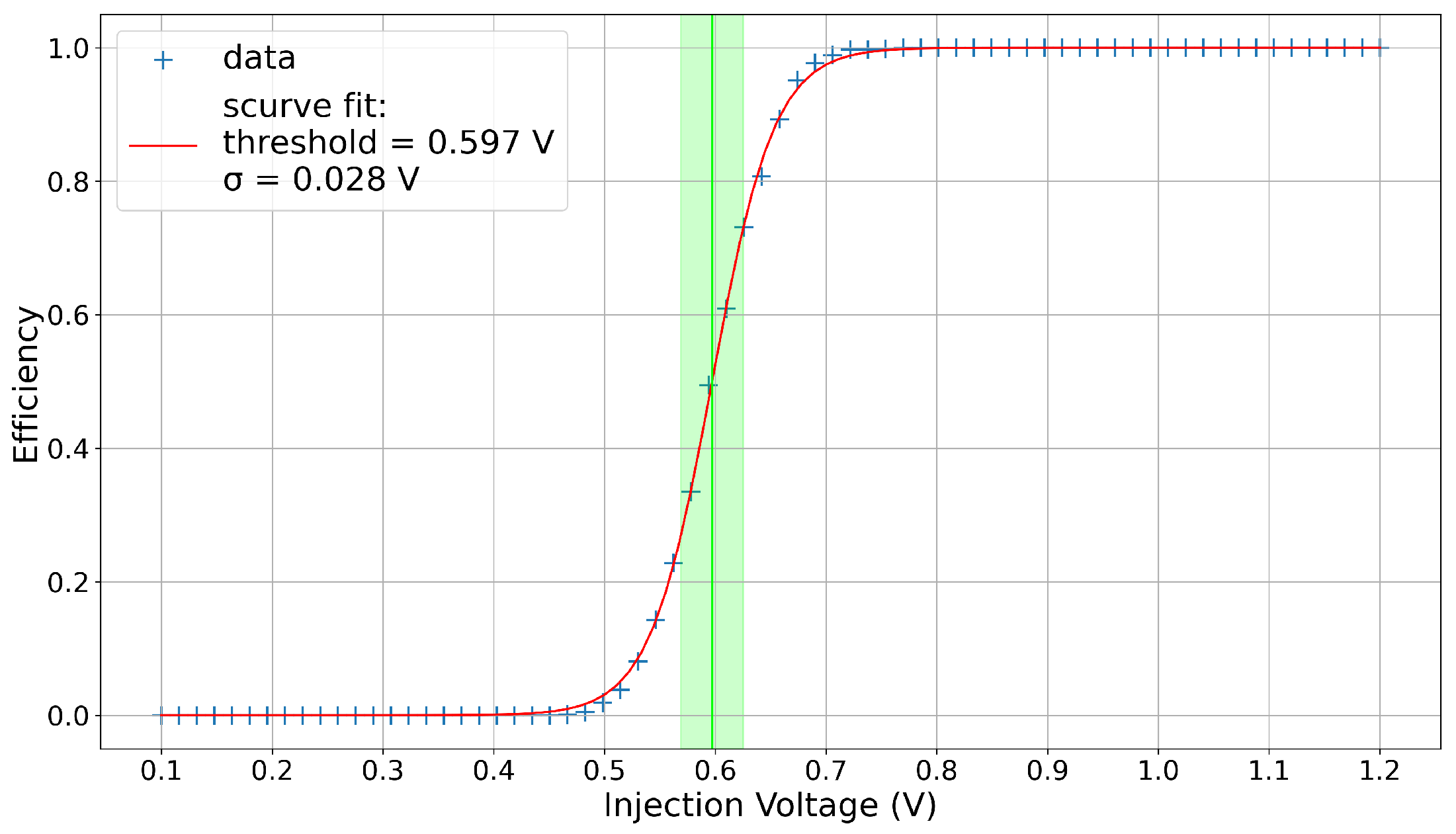
Ionizing particles are registered by the HitPix detector when the induced signal exceeds a programmable threshold. The signal height is not measured by the standard data processing chain. For debugging purposes, the analog signals of one row can be routed to a readout pad. To determine the noise of the pixel cells and to understand the response to electrical test signals, an external voltage pulse of varying amplitude can be injected into the pixel front-end. By scanning the amplitude of the injected signal at a fixed threshold, the pixel response and noise can be determined. The distribution follows an error-function and the noise corresponds to the width of the transition region. Figure 10 shows an example of such a measurement.
The general noise level of HitPix2 at the comparator stage is about 28  m V , while a typical signal from high-energy protons is about 200  m V . Knowing the noise level and the expected signal height of the relevant particles, one can set an optimal threshold, which eliminates hit counts due to noise, but still registers all particle transitions.
To verify that the chosen pixel size is adequate for the application, the cluster size was evaluated for different beam conditions. A cluster is a group of adjacent hits with its size defined as the number of pixel cells in this group. If the cluster size is close to one, the generated charge carriers are mainly localized within one pixel, which is advantageous for this counting application. The high particle rate of the beam and the implementation of the hit counting prevent easy evaluation of the single particle cluster size. The evaluation needs to be made in corners of the chip with very low particle rate and no pile-up in the frame, so that individual clusters do not merge into one large cluster. After analysis of the runs taken at HIT, only the cluster size for single carbon ions at a threshold of 170 mV can be stated with reasonable reliability as 2.4. The cluster size decreases with increasing thresholds (about 1.2 at 450 mV), and clusters with protons are expected to be smaller due to the smaller charge deposition.
These results show that the chosen pixel size is well adapted to the particle spectrum, but could also be increased, if other constraints like pixel capacitance and resolution do not stand in contradiction.

4.3. Radiation Tolerance

Detectors with different substrate resistivities were irradiated at the ZAG with 23  M e V protons up to a 1  M e V neutron equivalent fluence of 1 × 1015 cm−2. The uniform irradiation resulted in an increase of the leakage current as listed in Table 2.
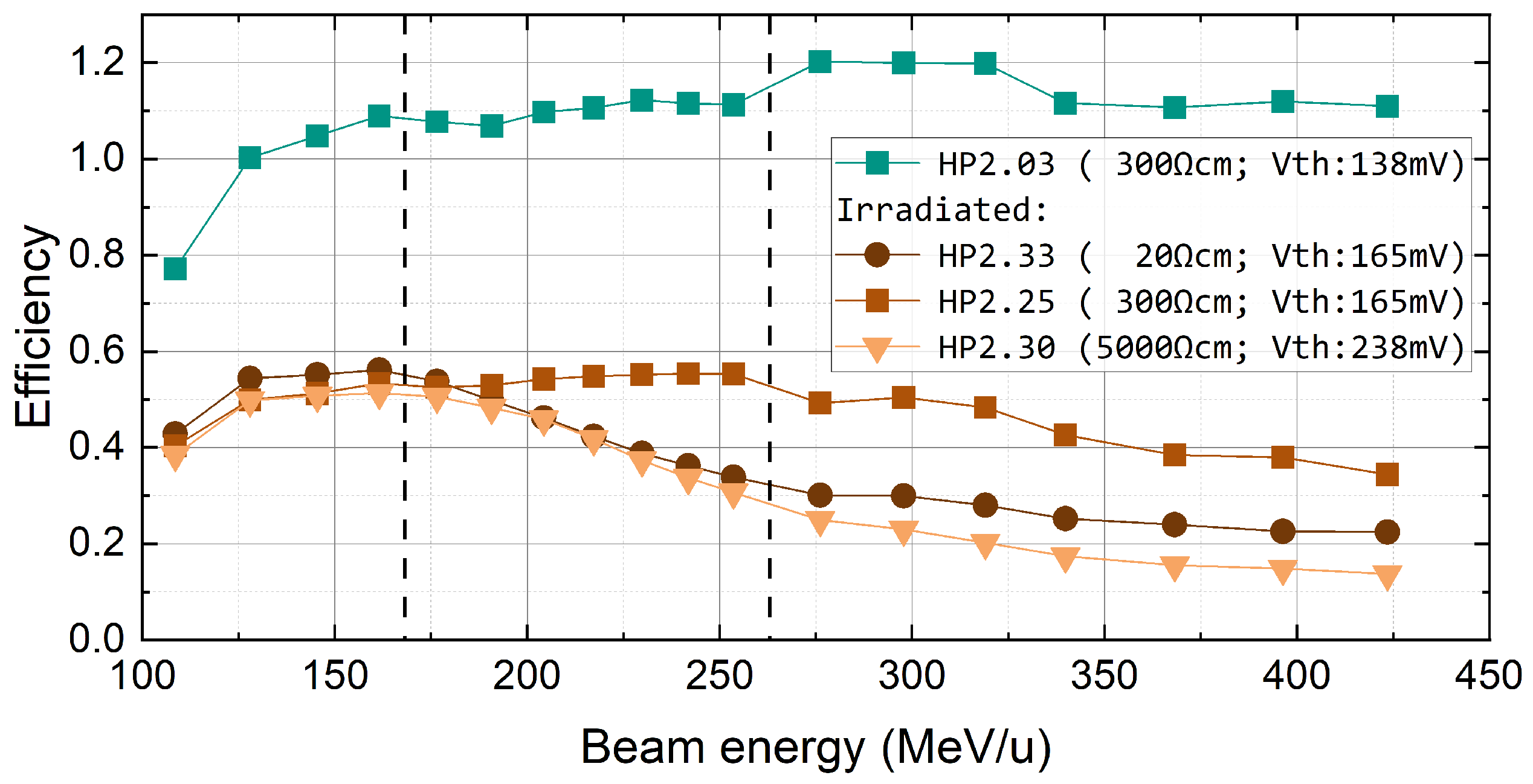
These irradiated detectors were exposed to a carbon ion beam at HIT with a defined intensity from which the total number of particles is derived (uncertainty of 5% on number of particles in the QA room; less than 2% in the treatment rooms). This number is compared to the number of acquired hits and the ratio is the hit detection efficiency quoted in Figure 11.
The hit detection efficiency of the unirradiated sample HP2.03 exceeds 100% since for each particle on average 1.14 hits are registered (Section 4.2). The uniformly irradiated detectors still work and detect the beam spot correctly. Compared to the unirradiated reference sample, the efficiency is reduced, which becomes more pronounced at higher ion energies, for which less ionization and, therefore, signal is expected. Since the results are based only on one sample each, one cannot draw a final conclusion on the best choice of substrate resistivity yet. There are further test conditions which have not been optimized so far. The irradiated samples were operated at room temperature and not cooled, which can lower the leakage current and noise. Therefore, the threshold was also possibly set too high so that the pixels were less sensitive to small signals. A further way to improve the efficiency is a higher bias voltage, which was limited to 25  V due to the high leakage current of the samples with the lowest resistivity in this comparative study.
In general, the detectors are operational after irradiation up to a fluence equivalent to one year’s operation at the central spot, but further tuning is required to keep the efficiency high, avoiding the need for overly frequent calibrations.

4.4. Beam Monitoring

Fast reconstruction of the beam position is one of the key requirements for a beam monitoring system. With the current HitPix2 detector, only an area of 9.6 mm× 9.6 mm is sensitive to particles and, therefore, only very tiny beam spots and small movements can be traced. Distortions of the reconstruction at the edges of the detector are expected and will not occur in the final system, since the missing beam spot part will be recorded by the surrounding detectors. 
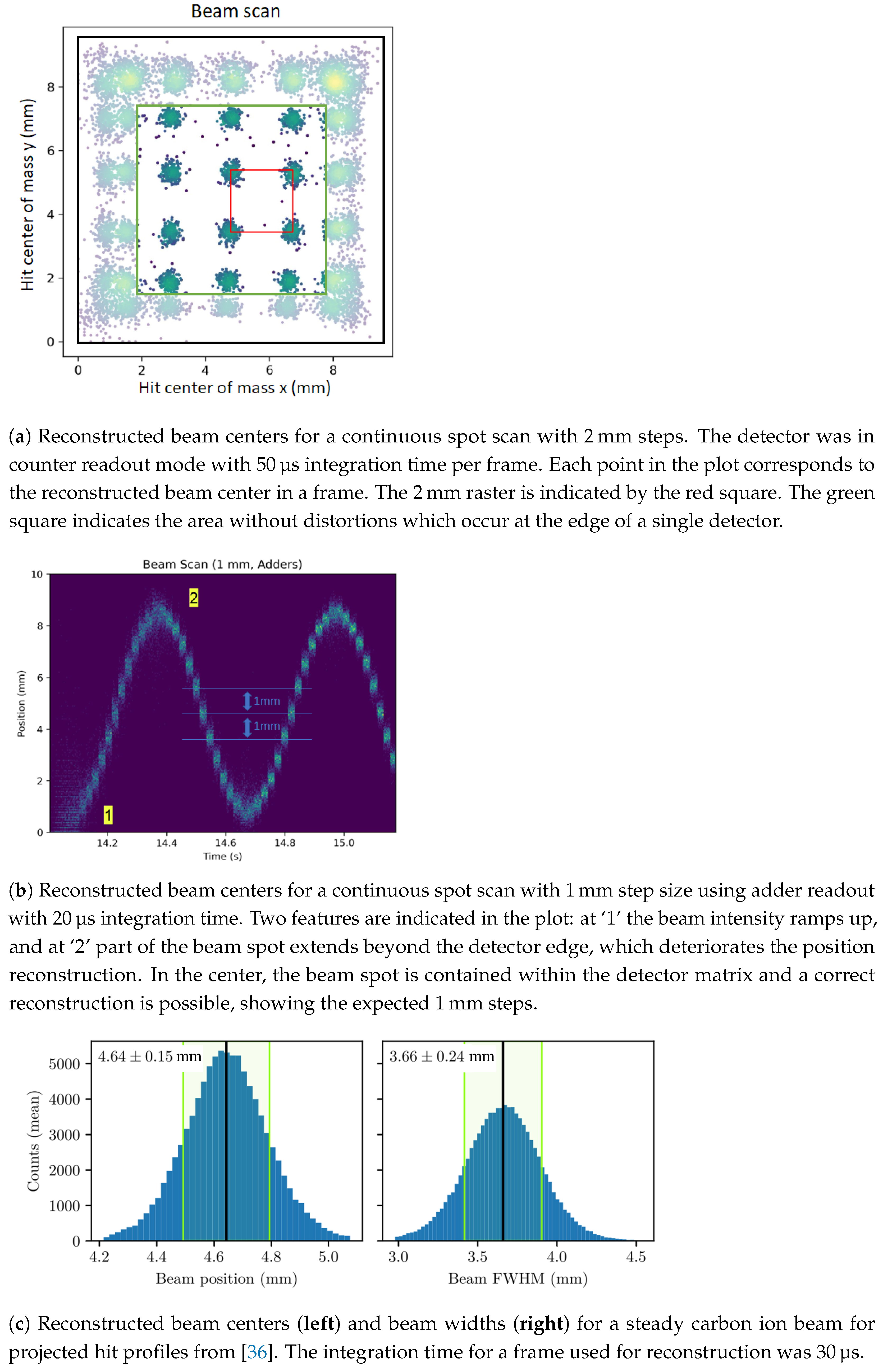
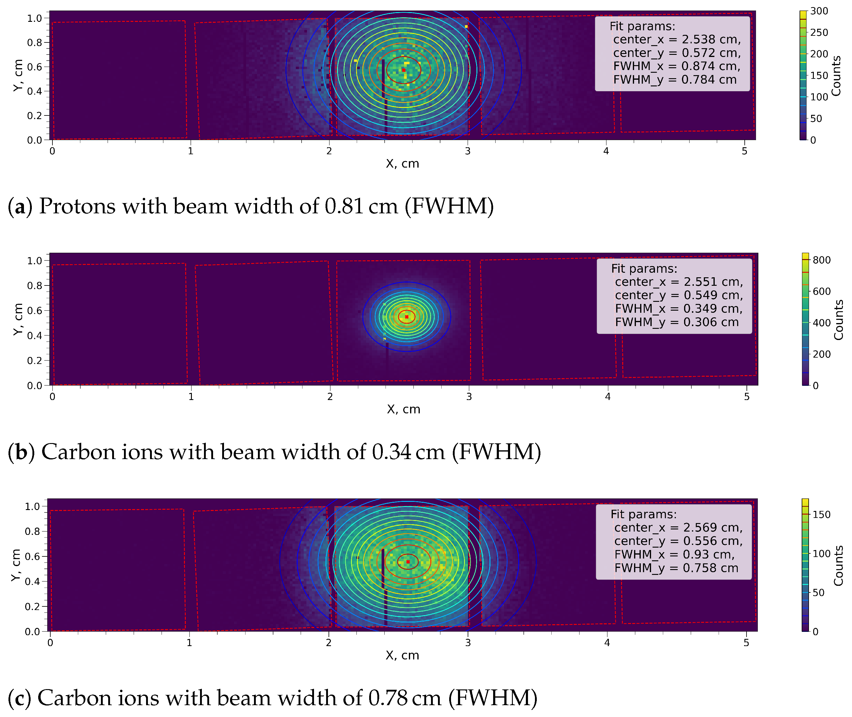
Figure 12a shows the reconstructed beam positions for a carbon ion beam with the smallest focus value possible at HIT.
Between each irradiation spot, the beam is moved by 2  m m . During one spot irradiation of several seconds length, the position is reconstructed many times from the hits acquired during a 50  μ s frame, and each of the reconstructed points is one entry in the histogram in Figure 12a. For the reconstruction of the beam spot, a simple mean algorithm is used, which can also be easily implemented on an FPGA. The projected hits are binned by pixels at positions x i , with number of hits n i . The mean beam position x 0 and beam width σ 0 (or full width half maximum FWHM) are calculated as
x 0 = 1 n tot i n i · x i
σ 0 2 = 1 n tot 1 i n i · x i x 0 2 ( FWHM = 2 2 ln 2 σ 0 ) .
In the center, one can clearly see the separation of 2  m m as intended for this irradiation plan. At the detector edges, the reconstructed position is distorted due to the missing particles outside the detector, as expected.
A special feature of the HitPix family is the projection of the hit counts on one axis (later two; adder readout mode). Figure 12b illustrates this feature. It shows the reconstructed positions of the projected beam profile integrated within 20  μ s during spot scanning irradiation. The small carbon ion beam spot was scanned in 1  m m steps. This demonstrates that in this acquisition mode, which will be the default during operation as beam monitor, the beam motion can be traced continuously without dead time during readout.
To investigate the precision of the reconstruction method, a steady beam of carbon ions was monitored for several seconds and the reconstructed position and width is represented in the two histograms in Figure 12c. The standard deviation or precision of the reconstructed position in this case is 150  μ m . Assuming a chip alignment precision of 10  μ m , which is a plausible value assuming an automatized pick and place procedure, the resulting position accuracy is below the required accuracy of 200  μ m . For the presented low intensity of 5 × 10⁶ s−1 and 30  μ s integration time, each projected beam profile contains about 150 hits on average, which limits reconstruction precision. Higher intensities result in higher precision, e.g., at 5 × 10⁷ s−1, precision is improved to 80  μ m .
The width of the beam is taken as the standard deviation of the hit distribution. From these measurements, a mean beam width of 3.66  m m (FWHM) is derived and indicated in Figure 12c (right). This is slightly higher than the nominal width of 3.4  m m , but still well within the allowed delivered width range of +25%/–10%.
In this section, we have demonstrated that with the HitPix detector it is possible to monitor beam position and width with the required accuracy. The short acquisition time of below 30  μ s allows rapid feedback, and the operation in projection mode allows for fast readout of the data, and, thus, low result latency.

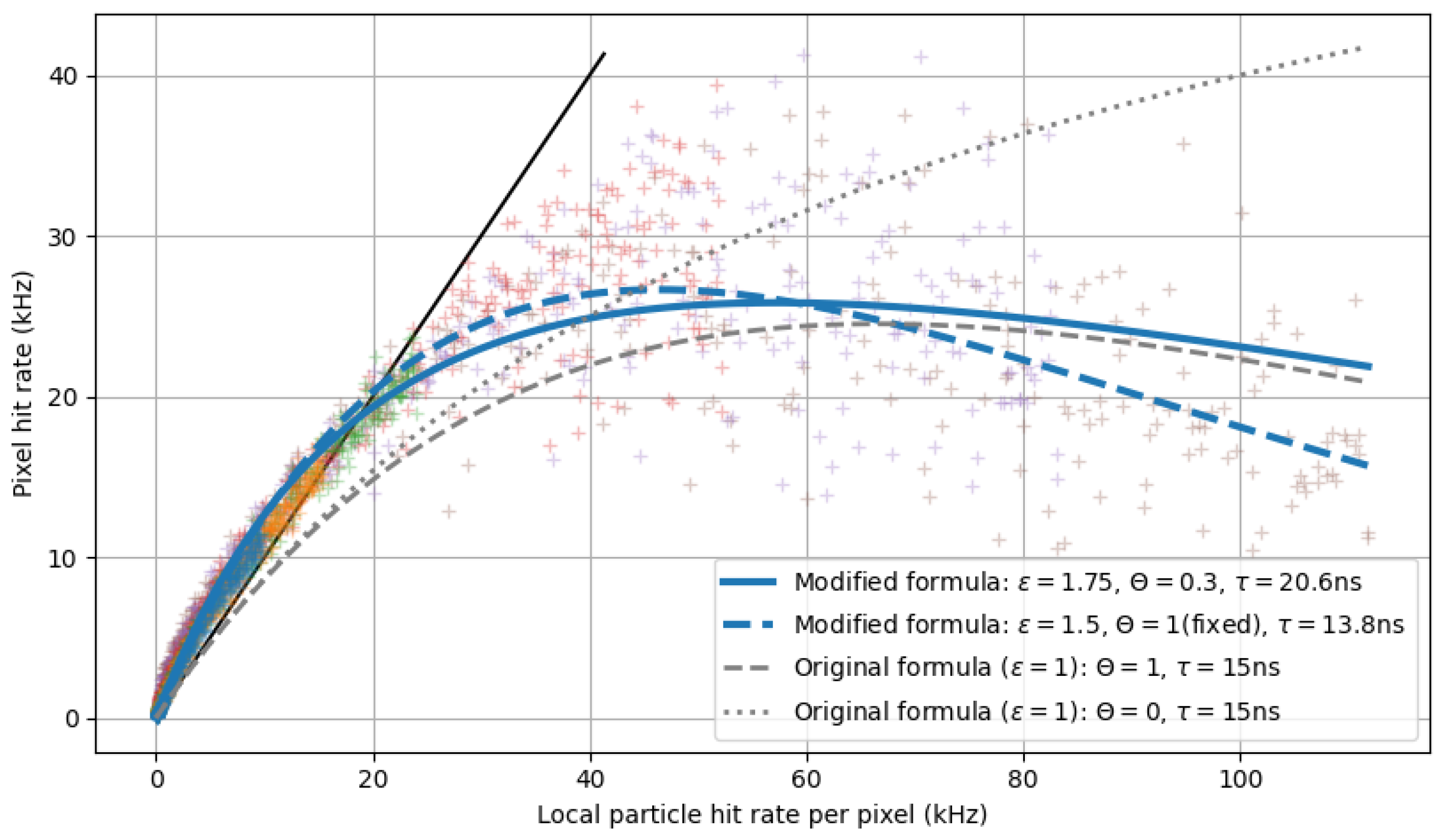
4.5. High-Rate Capability

The measurements presented so far have been mainly acquired at low beam intensities. This section focuses on the high-rate capability of the HitPix2 detector. To address this property, an intensity scan of a steady and small carbon ion beam at the highest energy was investigated. The expected local particle rate is calculated by the average intensity of the spot irradiation and the position of the pixel with respect to the beam center assuming a Gaussian beam profile. The registered hit rate versus the expected local particle rate for each pixel at several beam intensities is plotted in Figure 13.
At low intensities, the pixels register the expected number of hits, also considering that, on average, each particle generates 1.14 hits (Section 4.2). With increasing local particle rate, the registered hit rate saturates and a huge spread for individual pixels is observed. This effect can be modeled, taking dead time of the hit detection into account using a slightly modified version of Takacs’ formula [44]:
ν out = ϵ · ν · θ e ϵ · ν · θ · τ + θ 1
where ν out is the measured hit rate, ν the true particle rate, ϵ the hit efficiency (additional parameter to account for clusters), θ the probability of paralyzing dead time ( θ = 1 would be fully paralyzing, i.e., hits during dead time extend the dead time), and  τ is the dead time. The solid blue line in Figure 13 represents the result of a fit with all free parameters to the data, indicating a dead time of τ =  20.6  μ s . When forcing a fully paralyzing dead time, the curve fits the data equally well (slightly better at higher rates), resulting in τ =  13.8  μ s . This behavior is unexpected both from design and laboratory measurements and is not in compliance with the requirements. If the registered hit rate would follow a steady function with respect to the local particle rate, the hit rate could be corrected, but for dropping and widely scattered rates this is not possible.
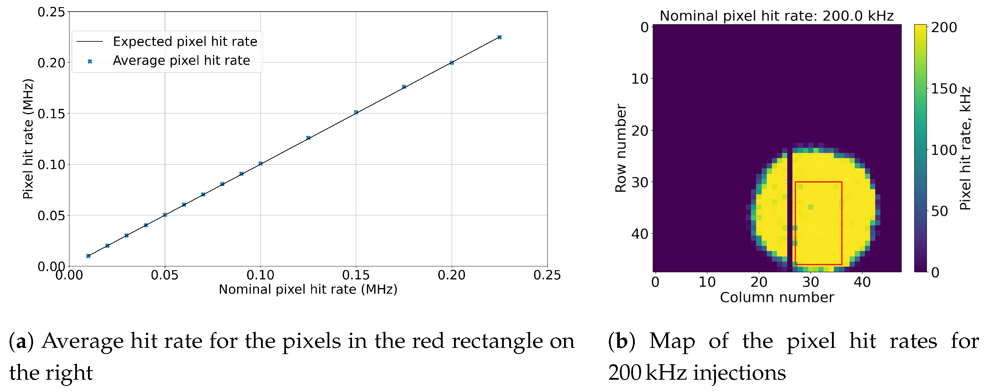
Further investigations were performed to understand this behavior. Short light pulses generated by a pulsed infrared LED were injected on the detector with increasing pulse frequency. The pixel counts were compared to the number of light pulses. For optimally illuminated pixels, the count rate follows the injection rate up to a rate of 225 kHz as shown in Figure 14.
In this configuration, the hit detection efficiency is very high up to much higher injection rates than in the ion beam in Figure 14. This indicates that the fast counting capability of the pixels is functioning.
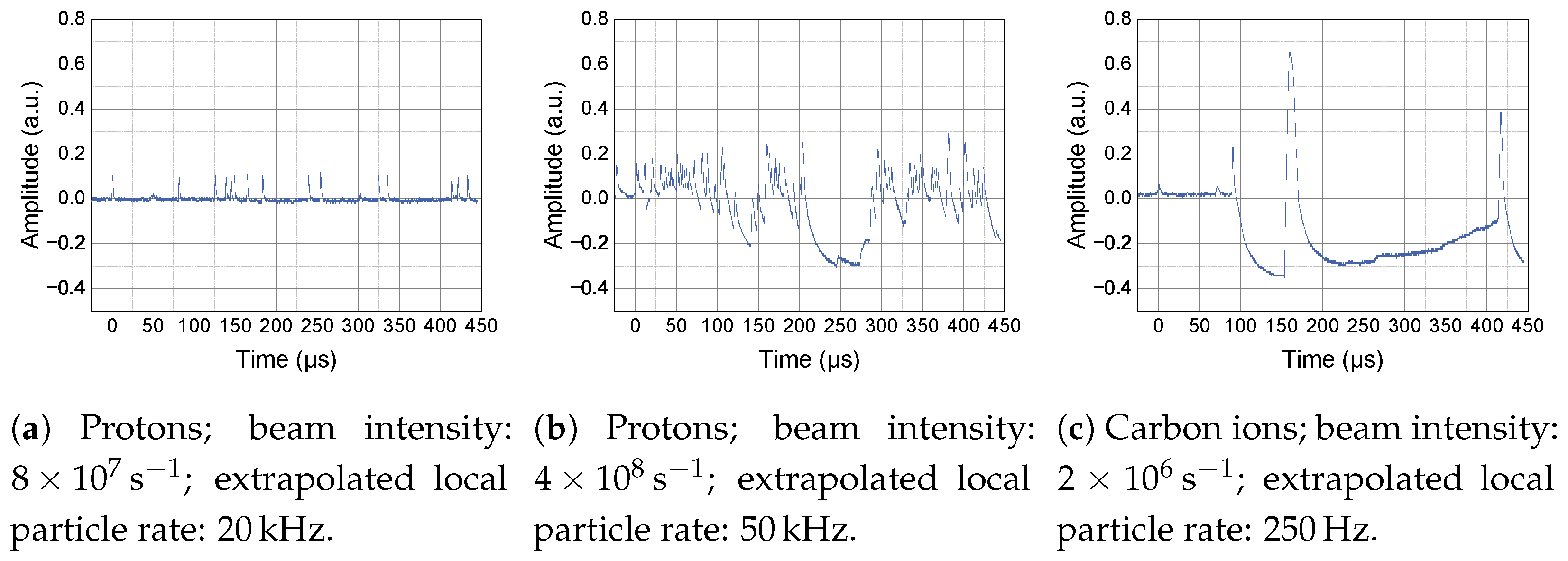
Looking at the analog signals of the amplifier of a pixel in the ion beam, we observe an increasing number of dips of the baseline voltage when exposed to higher particle rates. Figure 15 shows examples of such measurements.
Carbon ions generate the most severe, but less frequent, dips. During the time the baseline is reduced, no hits are detected, causing dead time.
These measurements suggest that the heavily ionizing ions influence the functioning of the pixels when a certain region in the pixel cell is hit. In addition, analog signals were recorded of injected alpha particles with an energy of about 5.5 MeV from an Am-241 source. Similar baseline voltage drops as in the ion beam could be provoked with these alpha particles. By placing the source above different locations of the detector, it could be excluded that the electronics in the periphery are affected.
In conclusion, the hit detection efficiency of the HitPix2 drops for high-rate particle beams. The investigations indicate that at a high rate of highly ionizing particles, the baseline voltage is affected and hit detection deteriorates. Still, the pixel cells function as expected for moderate charge injection and further work can concentrate on mitigating effects induced by highly ionizing particles. If the high-rate capability is not improved in a following version of the detector, the beam monitoring requirements cannot be met.

4.6. Magnetic Field Tolerance

Magnetic fields are required for MRI-guided radiotherapy, however, they influence the movement of charged particles and charge carriers in solids. Since all modern detector technologies in beam monitoring rely at least partially on electric fields and movement of charge carriers, the operation within the strong magnetic field of an MRI machine or the somewhat lower fringe field of a scanner has to be part of the technology evaluation process. There are two application cases for a beam monitoring device:
  • Continuous monitoring during the irradiation at the beam exit about 1  m away from the center of the MRI;
  • Diagnostics of the beam shape in the center of the MRI.
Although not necessary for the first case, we also study the second application case.
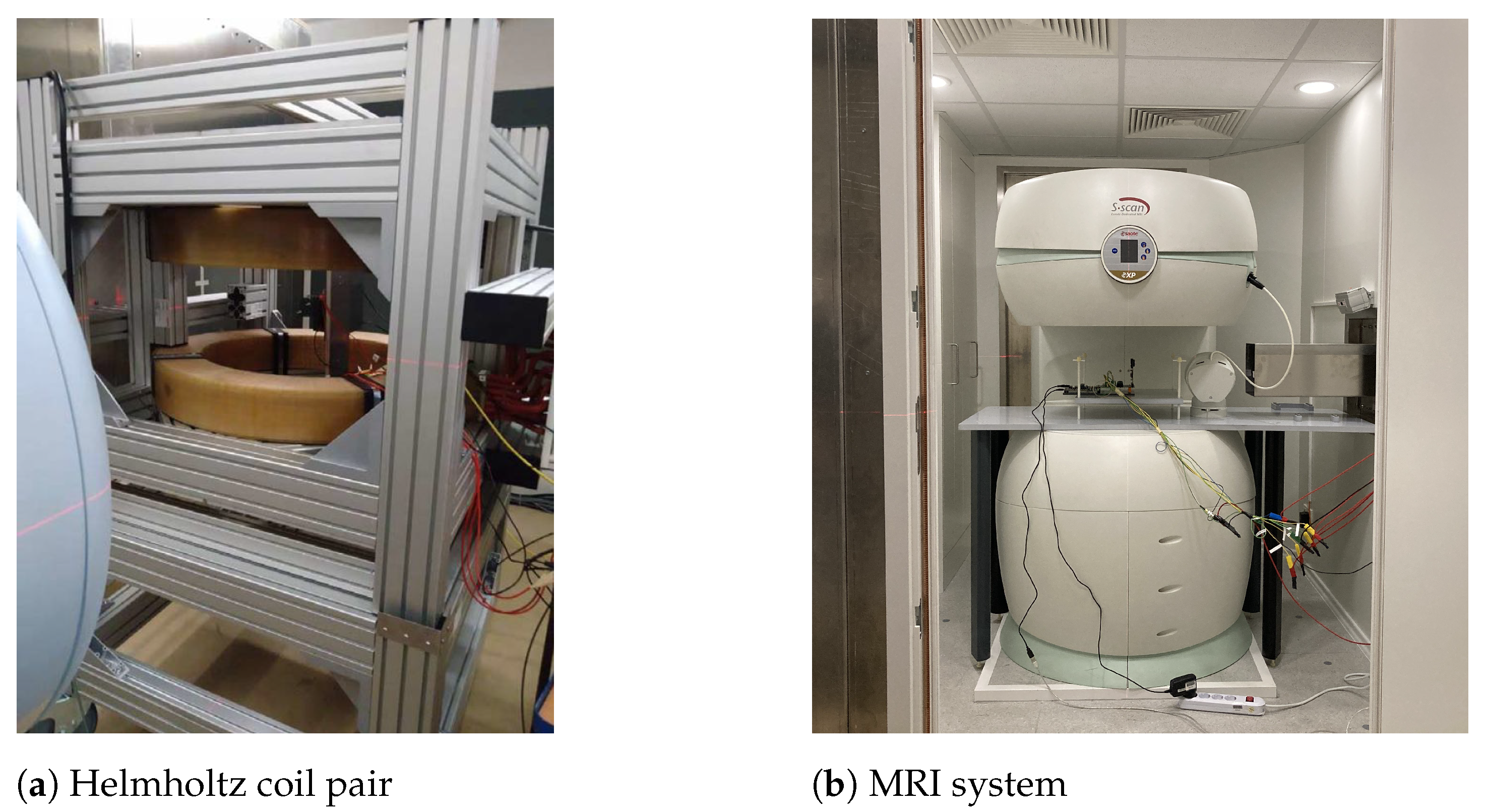
In a first step, we investigated the performance of a detector setup with HitPix1 in the adjustable field of the Helmholtz coils as described in Section 3.2. Unfortunately, but as expected, the commercial FPGA board has several components (mainly voltage regulation) which cannot be operated in magnetic fields. Therefore, the readout stopped already at a 60  m T field. Up to this field strength, the detector kept working and no performance degradation in monitoring a carbon ion beam was detected.
To cope with the sensitivity of the FPGA board for these tests, a PCIe x16 twisted-pair riser cable with 1:1 connectivity was designed and produced. Using this cable, the commercial readout electronics were moved out of the field center and the detector readout worked up to 100  m T , which is the maximum possible field of the Helmholtz-coil pair.
For MRI tests, the modified setup with riser cable and HitPix2 was used. The detector carrier PCB was placed in the middle of the MRI (described in Section 3.2) and the readout FPGA board at a distance of approximately 1  m . No influence of the static magnetic field was observed in this configuration. The rapidly changing field of the scanning MRI, however, caused the detector to lose its configuration, rendering it non-operational. The reason for the configuration loss is the high induced voltage on the detector’s configuration lines. Depending on the MRI scanning procedure, we measured pulses of several volts on these lines, while the logic levels are about 1.8  V . At a distance of 35  c m from the center of the scanning MRI (approximately one quarter of the central field strength), the detector kept its configuration and readouts worked normally.
In the next iteration of the detector, a lockable configuration is foreseen, meaning that random noise on the configuration line will be ignored and only configuration bits preceded by an unlock-code will be accepted.

4.7. Multi-Detector Readout

To reach the required large size of the beam monitor, it is necessary to read out many detectors. HitPix2 implements two schemes for multi-detector readout. In daisy chain mode, several detectors can be directly interconnected (digital data_out to data_in) and the data shifted through all of them. The other mode is a bus configuration for which several detectors can be connected to a common data line and the detectors individually selected for readout.
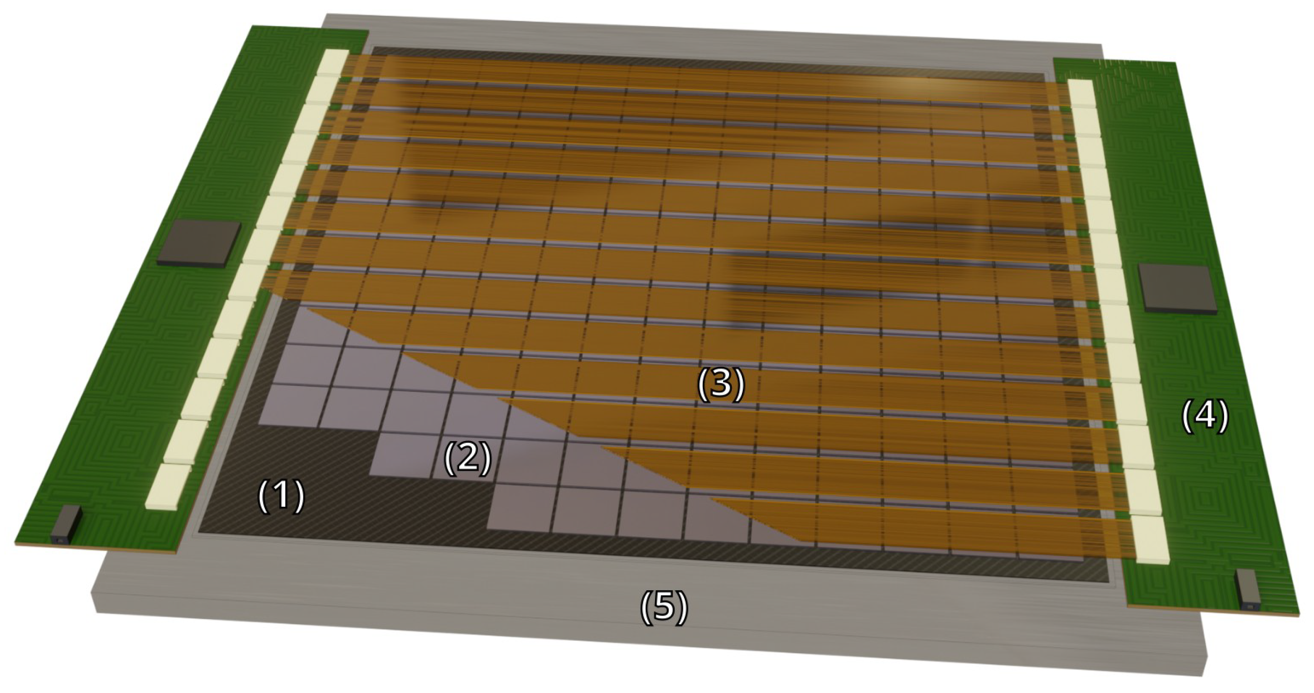
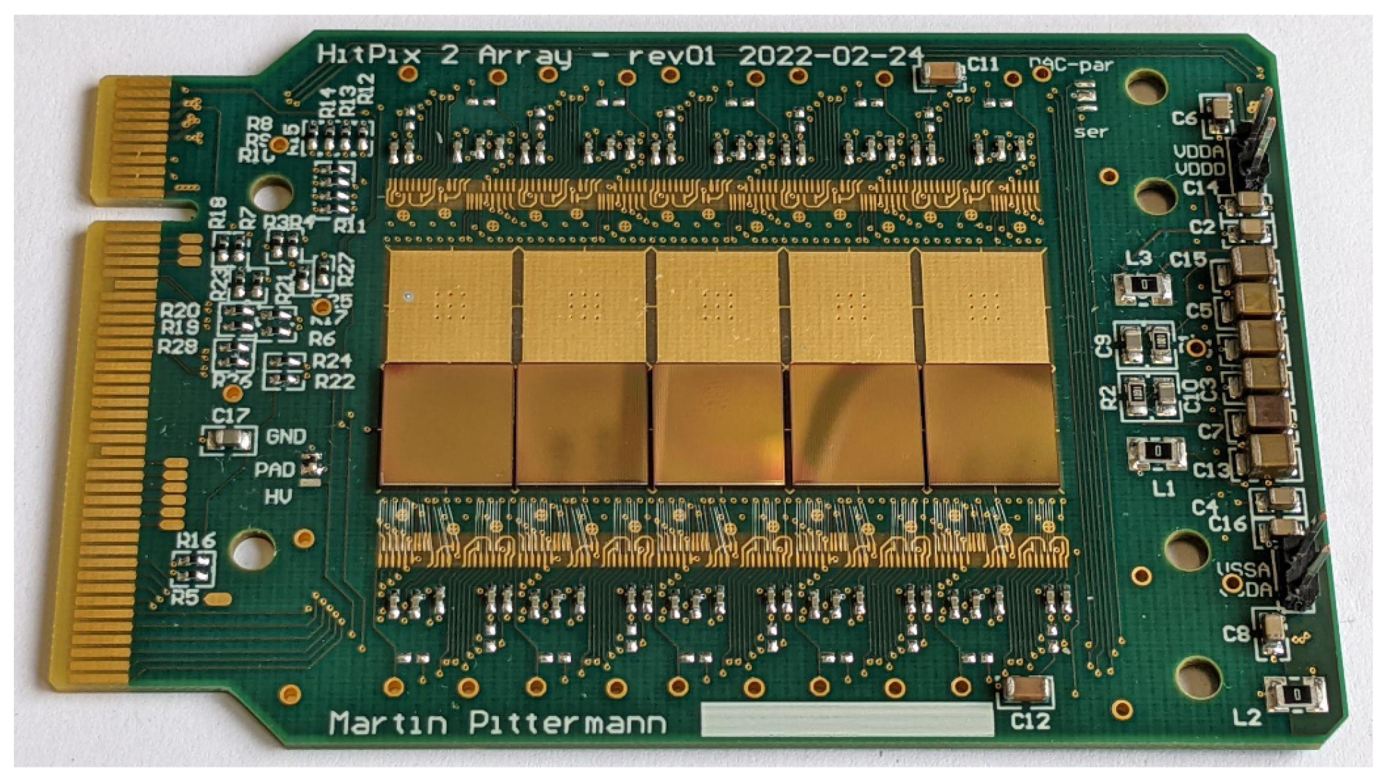
A PCB was designed to validate these functionalities in a 2 × 5 matrix (Figure 16).
A first PCB was equipped with five detectors in one row. The detectors were successfully read out in both readout modes. At HIT, the matrix was exposed to particle beams for different beam parameter settings. The collected hit counts for three beam settings are shown in Figure 17.
The reconstructed beam spot widths are well in agreement with the nominal settings. Especially in the bottom plot, a smooth transition of hit counts from one detector chip to the next can be observed. This demonstrates the comparable hit detection efficiency of the neighboring detectors.
To achieve very high readout rates, the bus configuration should be used since the daisy chain readout showed a limit of about 28 Mbit s−1 on the test setup.

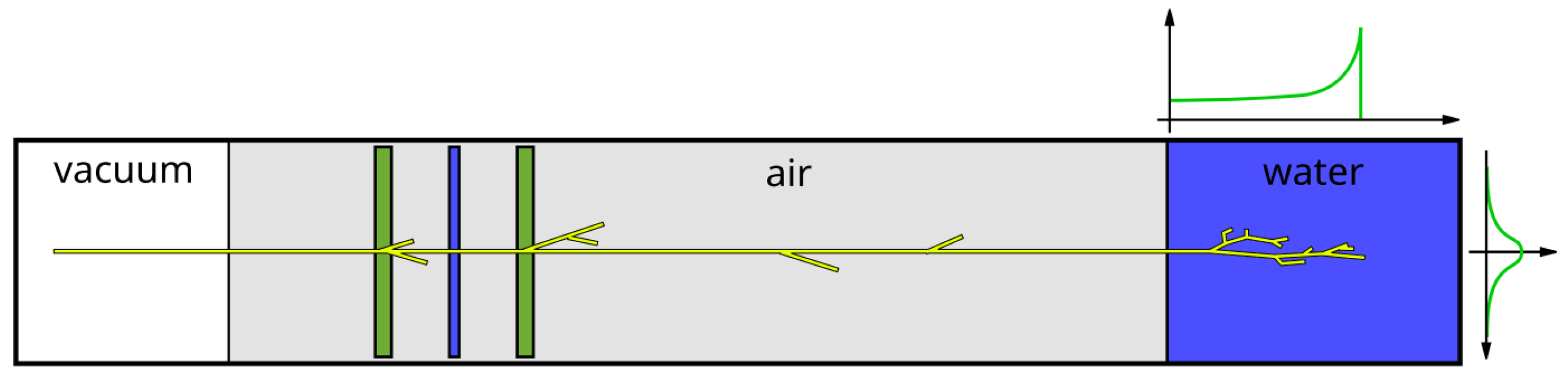
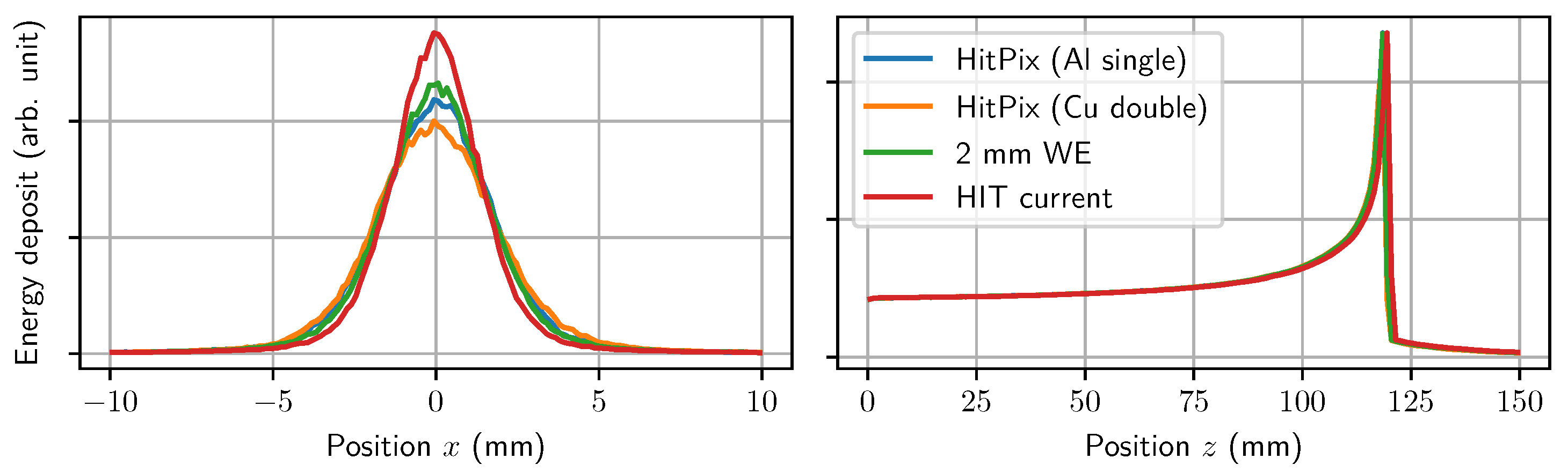
4.8. Simulation Results

With the simulation environment described in Section 3.4, ion trajectories were generated and the spatial distribution of the energy deposition was recorded. The resulting profiles are compared in Figure 18 for the current system at HIT, with a water equivalent of 2  m m , which is the specified maximum material for five layers (Section 1.2), and the HitPix system in two variants: with a single-layer flex cable made of aluminum traces, and with a double-layer flex cable made of copper traces.
The distributions do not show significant deviations. As expected, the current system with gas chambers does not affect the low energy carbon beam as much as the solid state approach. Still, the additional broadening of the beam is not very large if one avoids copper traces.
Table 3 summarizes the extracted FWHM for the four scenarios. At low energy, the envisaged arrangement HitPix (Al single) broadens the carbon ion beam by about 5% more than the 2  m m water equivalent, which represents a tolerable material budget. The almost homogeneous material distribution of the proposed detector is an advantage compared to the tungsten wires in MWCs, which act as strong scattering centers.
The HitPix detectors have a very small periphery to cover a maximally sensitive area. Still, manufacturing aspects cannot avoid a small insensitive region at three edges of the detector of 150  μ m , and at the fourth side the end-of-column electronics (128  μ m ) together with the contact pad region (260  μ m ) add up to a width of about 400  μ m . Further, the side-by-side placement of the detectors adds a small gap of about 100  μ m . In summary, there can be insensitive gaps of up to 500  μ m every 20  m m , which is the final detector chip dimension. To study the effect of a worst case gap of 600  μ m (equivalent to three missing pixel columns) on the beam spot reconstruction, a simulation of the hit distribution for various Gaussian beam shapes and positions was performed. Charge sharing has been taken into account by a constant probability of creating secondary hits next to the primary hits. Figure 19a shows two examples of the beam shapes with the gap at around position 2.5.
Distributions following such shapes are generated by Poisson random numbers for an average intensity of 2 × 10⁶ s−1 and 100  μ s integration time. In Figure 19b, the mean and standard deviation of the reconstructed position from 1500 frames is plotted in dependence of the beam distance to the gap applying two different reconstruction algorithms. The simple mean algorithm is visualized by the dashed lines, while the solid lines represent the results of a likelihood fit with a Gaussian function. The upper plot shows the average deviation (bias) which is the offset of the reconstructed position compared to the true position. It is mainly unaffected for the likelihood fit, while the simple mean algorithm has a maximum bias of close to 200  μ m when the gap lies in the beam spot tails, breaking the symmetry. A systematic shift in the position information for the feedback loop has to be avoided otherwise the uniform irradiation may be degraded. The standard deviation (SD) of the beam spot position in the lower plot of Figure 19b shows no significant difference between the algorithms. Wider beams result in a worse standard deviation or uncertainty due to the reduced hit counts per pixel.
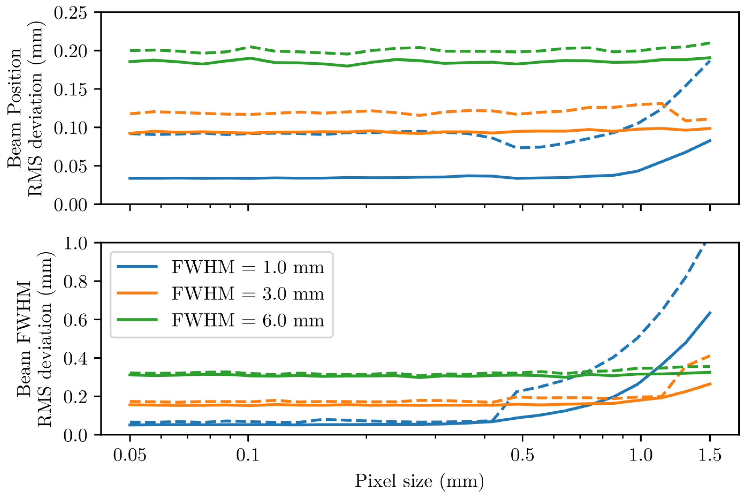
The appropriate dimensioning of the pixels to mainly record single-pixel clusters was validated by measuring the cluster size in Section 4.2. With the simulation framework introduced above, the effect of the pixel dimensions on the precision of the reconstructed beam position and width was investigated. The results are shown in Figure 20 for different beam widths, pixel sizes and algorithms.
These plots demonstrate that pixel sizes below 400  μ m result in similar uncertainties even for beams as narrow as 1 mm and can be implemented in the detector. Therefore, the pixel size can be adapted to other constraints like readout speed, diode capacitance or power consumption.

5. Summary and Conclusions

This article describes a new detector system based on hit counting HV-CMOS detectors which targets the use as a beam monitor for ion therapy. The detector is tailored to the requirements of the beam monitoring system at the Heidelberg Ion Beam Therapy center.
The pixel size is adapted to the resolution requirements. The hit counting capability and the built-in projections aim for processing high particle rates and fast readout at minimum latency. Attention was devoted to avoiding inactive areas and achieving low power consumption.
In several studies, the properties of the detector in view of the requirements as a beam monitor have been investigated. The resolution of the beam position and spot width for small beam spots were well within the requirements of 200  μ m accuracy. Hits from the particle beam can be recorded continuously with an integration time of 20  μ s and the scanned beam can be traced.
The HV-CMOS detectors were irradiated to a fluence corresponding to the maximum expected fluence in the center of the beam monitor after one year. The irradiated samples did work in a carbon ion beam with reduced hit detection efficiency, which could be corrected for after calibration. There are options to improve the performance, like optimizing the threshold, cooling the detectors and operating at higher bias voltage, which could extend the period for calibrations.
Measurements with high-rate ion beams revealed a hit rate limiting effect, which is being investigated. A likely cause are heavily ionizing particles generating and accumulating charge below the cell electronics, which cause the baseline voltage to drop, making following hits undetectable. This failure mode will be further analyzed and corrected in the next version. One possible correction would be to modify the feedback circuit to enable the baseline to be restored faster.
The detectors were also tested in magnetic fields and demonstrated tolerance of static magnetic fields of at least 250  m T . The rapidly changing fields of a scanning MRI induced high voltages in the connecting cables, which were not optimized for this application yet. In some scanning modes, these voltage pulses on the configuration lines made operation in a scanning MRI system impossible. The next version of the detector chip will have lockable configuration registers.
A first step towards a large matrix of HitPix detectors was the production and partial assembly of a PCB providing supply and data lines for up to ten chips. The daisy chain and bus readout modes were tested successfully and the matrix recorded particle beams at HIT. The reconstructed beam spot widths are well in agreement with the nominal beam settings.
In addition to measurements with the detectors, several simulation studies were performed. The impact of the solid-state detector on the scattering of the beam is close to the specified upper limit of 2  m m water equivalent, and has the advantage that concentrated scattering centers, like the wires of the multi-wire chambers, are not present. The effect on position resolution with unavoidable gaps of the sensitive area between detector chips was studied. In a worst-case scenario with 600  μ m gaps and a very narrow beam of 1  m m (FWHM), the bias of the position reaches 200  μ m at the worst position about 400  μ m away from the gap. This is true for a simple algorithm calculating the mean of the hit distribution. A likelihood fit of a Gaussian function would not be affected at all by the gaps and, although challenging, will be considered for implementation on an FPGA. In another simulation, it was shown that pixel sizes up to 400  μ m show similar and adequate reconstruction accuracy of the beam spot with a width down to 1 mm.
In summary, the investigated HitPix2 detector has proven to be a promising candidate for a beam monitoring system at an ion beam facility. The shortcomings identified during laboratory and beam tests are being addressed and a successor is in development. The next HitPix version will feature offset tuning, the second projection direction, faster readout concept, and increased tolerance against single-event and charge-up effects. The next step is to assemble a matrix as envisioned in Section 1.4 but with a reduced number of 5 × 5 chips. This detector system will be used for long-term operation tests in the quality assurance room at HIT.

Author Contributions

Conceptualization, A.D., I.P., A.W. and J.D.; Data curation, M.P.; Formal analysis, M.P., B.T., T.H. and J.N.; Funding acquisition, A.D., F.E., U.H., I.P., J.D., N.G., O.J. and S.K.; Investigation, F.E., R.K., M.P., B.T., A.W. and J.N.; Project administration, A.D. and U.H.; Resources, F.E., I.P., M.P., A.W., S.B. and J.N.; Software, F.E. and M.P.; Supervision, M.B., U.H., I.P. and S.K.; Validation, A.D. and J.N.; Visualization, F.E., M.P. and B.T.; Writing—original draft, A.D. and F.E.; Writing—review and editing, U.H., R.K., N.G., T.H., O.J. and J.N. All authors have read and agreed to the published version of the manuscript.

Funding

This research was funded by the Heidelberg Karlsruhe Strategic Partnership (HEiKA), the KIT Center Elementary Particle and Astroparticle Physics (KCETA), Helmholtz Program Matter and Technology, German Federal Ministry of Education and Research within the programm “Bildgeführte Diagnostik und Therapie—Neue Wege in der Intervention” under Grant 13GW0436A (ARTEMIS). We acknowledge support by the KIT-Publication Fund of the Karlsruhe Institute of Technology.

Data Availability Statement

The data presented in this study are available on request from the corresponding author. The data are not publicly available due to the involved calibration procedures.

Acknowledgments

The authors would like to thank Rudolf Schimassek for his contribution to the DAQ system and GECCO board, Horacio Mateos for the assembly and bonding and Bernd Berger for performing the irradiations at the cyclotron.

Conflicts of Interest

The authors declare no conflict of interest. The funders had no role in the design of the study; in the collection, analyses, or interpretation of data; in the writing of the manuscript, or in the decision to publish the results.

References

  1. Jäkel, O.; Kraft, G.; Karger, C.P. The History of Ion Beam Therapy in Germany. Z. Für Med. Phys. 2022, 32, 6–22. [Google Scholar] [CrossRef]
  2. Royce, T.J.; Efstathiou, J.A. Proton Therapy for Prostate Cancer: A Review of the Rationale, Evidence, and Current State. Urol. Oncol. Semin. Orig. Investig. 2019, 37, 628–636. [Google Scholar] [CrossRef]
  3. Haberer, T.; Debus, J.; Eickhoff, H.; Jäkel, O.; Schulz-Ertner, D.; Weber, U. The Heidelberg Ion Therapy Center. Radiother. Oncol. 2004, 73, S186–S190. [Google Scholar] [CrossRef] [PubMed]
  4. Haberer, T.; Becher, W.; Schardt, D.; Kraft, G. Magnetic Scanning System for Heavy Ion Therapy. Nucl. Instrum. Methods Phys. Res. Sect. A Accel. Spectrom. Detect. Assoc. Equip. 1993, 330, 296–305. [Google Scholar] [CrossRef]
  5. Galonska, M.; Scheloske, S.; Brons, S.; Cee, R.; Höppner, K.; Mosthaf, J.; Peters, A.; Haberer, T. The Hit Gantry: From Commissioning to Operation. In Proceedings of the IPAC 2013: Proceedings of the 4th International Particle Accelerator Conference, Shanghai, China, 12–17 May 2013; pp. 3636–3638. [Google Scholar]
  6. Schömers, C.; Feldmeier, E.; Haberer, T.; Naumann, J.; Panse, R.; Peters, A. Patient-Specific Intensity-modulation of a Slowly Extracted Beam at the HIT Synchrotron. In Proceedings of the IPAC 2013, Shanghai, China, 12–17 May 2013; pp. 2944–2946. [Google Scholar]
  7. Hoffmann, A.; Oborn, B.; Moteabbed, M.; Yan, S.; Bortfeld, T.; Knopf, A.; Fuchs, H.; Georg, D.; Seco, J.; Spadea, M.F.; et al. MR-guided Proton Therapy: A Review and a Preview. Radiat. Oncol. 2020, 15, 129. [Google Scholar] [CrossRef]
  8. Sauli, F. Principles of Operation of Multiwire Proportional and Drift Chambers; CERN Yellow Report; CERN: Geneva, Switzerland, 1977. [Google Scholar] [CrossRef]
  9. Lin, S.; Boehringer, T.; Coray, A.; Grossmann, M.; Pedroni, E. More than 10 Years Experience of Beam Monitoring with the Gantry 1 Spot Scanning Proton Therapy Facility at PSI. Med. Phys. 2009, 36, 5331–5340. [Google Scholar] [CrossRef]
  10. Giordanengo, S.; Manganaro, L.; Vignati, A. Review of Technologies and Procedures of Clinical Dosimetry for Scanned Ion Beam Radiotherapy. Phys. Medica 2017, 43, 79–99. [Google Scholar] [CrossRef]
  11. Wang, Z.; Zou, S.; Fan, Y.; Liu, J.; Sun, X.; Wang, D.; Kang, H.; Sun, D.; Yang, P.; Pei, H.; et al. A Beam Monitor Using Silicon Pixel Sensors for Hadron Therapy. Nucl. Instrum. Methods Phys. Res. Sect. A Accel. Spectrom. Detect. Assoc. Equip. 2017, 849, 20–24. [Google Scholar] [CrossRef]
  12. Actis, O.; Meer, D.; König, S. Precise On-Line Position Measurement for Particle Therapy. J. Instrum. 2014, 9, C12037. [Google Scholar] [CrossRef]
  13. Klimpki, G.; Psoroulas, S.; Bula, C.; Rechsteiner, U.; Eichin, M.; Weber, D.C.; Lomax, A.; Meer, D. A Beam Monitoring and Validation System for Continuous Line Scanning in Proton Therapy. Phys. Med. Biol. 2017, 62, 6126–6143. [Google Scholar] [CrossRef] [PubMed]
  14. Papa, A. Scintillating Fibres Coupled to Silicon Photomultiplier Prototypes for Fast Beam Monitoring and Thin Timing Detectors. Nucl. Instrum. Methods Phys. Res. Sect. A Accel. Spectrom. Detect. Assoc. Equip. 2016, 824, 128–130. [Google Scholar] [CrossRef]
  15. Ortega Ruiz, I.; Fosse, L.; Franchi, J.; Frassier, A.; Fullerton, J.; Kral, J.; Lauener, J.; Schneider, T.; Spanggaard, J.; Tranquille, G. A Multipurpose Scintillating Fibre Beam Monitor for the Measurement of Secondary Beams at CERN. In Proceedings of the 7th International Beam Instrumentation Conference, Shanghai, China, 9–13 September 2018; p. 4. [Google Scholar] [CrossRef]
  16. Allegrini, O.; Cachemiche, J.P.; Caplan, C.P.C.; Carlus, B.; Chen, X.; Curtoni, S.; Dauvergne, D.; Negra, R.D.; Gallin-Martel, M.L.; Hérault, J.; et al. Characterization of a Beam-Tagging Hodoscope for Hadrontherapy Monitoring. J. Instrum. 2021, 16, P02028. [Google Scholar] [CrossRef]
  17. Joram, C.; Uwer, U.; Kirn, T.; Leverington, B.D.; Bachmann, S.; Ekelhof, R.J.; Müller, J. LHCb Scintillating Fibre Tracker Engineering Design Review Report: Fibres, Mats and Modules; Technical Report LHCb-PUB-2015-008; CERN: Geneva, Switzerland, 2015. [Google Scholar]
  18. Leverington, B.; Dziewiecki, M.; Renner, L.; Runze, R. A Prototype Scintillating Fibre Beam Profile Monitor for Ion Therapy Beams. J. Instrum. 2018, 13, P05030. [Google Scholar] [CrossRef]
  19. Martišíková, M.; Hesse, B.M.; Nairz, O.; Jäkel, O. Test of an Amorphous Silicon Detector in Medical Proton Beams. Nucl. Instrum. Methods Phys. Res. Sect. A Accel. Spectrom. Detect. Assoc. Equip. 2011, 633, S259–S261. [Google Scholar] [CrossRef]
  20. Sacchi, R.; Ganjeh, Z.A.; Arcidiacono, R.; Attili, A.; Cartiglia, N.; Donetti, M.; Fausti, F.; Ferrero, M.; Giordanengo, S.; Ali, O.H.; et al. Test of Innovative Silicon Detectors for the Monitoring of a Therapeutic Proton Beam. J. Phys. Conf. Ser. 2020, 1662, 012002. [Google Scholar] [CrossRef]
  21. Vignati, A.; Donetti, M.; Fausti, F.; Ferrero, M.; Giordanengo, S.; Ali, O.H.; Villarreal, O.A.M.; Milian, F.M.; Mazza, G.; Monaco, V.; et al. Thin Low-Gain Avalanche Detectors for Particle Therapy Applications. J. Phys. Conf. Ser. 2020, 1662, 012035. [Google Scholar] [CrossRef]
  22. Krüger, W.; Bergauer, T.; Galatyuk, T.; Hirtl, A.; Kedych, V.; Kis, M.; Linev, S.; Michel, J.; Pietraszko, J.; Pitters, F.; et al. LGAD Technology for HADES, Accelerator and Medical Applications. Nucl. Instrum. Methods Phys. Res. Sect. A Accel. Spectrom. Detect. Assoc. Equip. 2022, 1039, 167046. [Google Scholar] [CrossRef]
  23. Flynn, S.; Manolopoulos, S.; Rompokos, V.; Poynter, A.; Toltz, A.; Beck, L.; Ballisat, L.; Velthuis, J.; Allport, P.; Green, S.; et al. Monitoring Pencil Beam Scanned Proton Radiotherapy Using a Large Format CMOS Detector. Nucl. Instrum. Methods Phys. Res. Sect. A Accel. Spectrom. Detect. Assoc. Equip. 2022, 1033, 166703. [Google Scholar] [CrossRef]
  24. Hartmann, F. Semiconductor Sensors. Nucl. Instrum. Methods Phys. Res. Sect. A Accel. Spectrom. Detect. Assoc. Equip. 2011, 628, 40–49. [Google Scholar] [CrossRef]
  25. Bruzzi, M. Novel Silicon Devices for Radiation Therapy Monitoring. Nucl. Instrum. Methods Phys. Res. Sect. A Accel. Spectrom. Detect. Assoc. Equip. 2016, 809, 105–112. [Google Scholar] [CrossRef]
  26. Hartmann, F. Evolution of Silicon Sensor Technology in Particle Physics; Springer: New York, NY, USA, 2017. [Google Scholar]
  27. Lutz, G. Semiconductor Radiation Detectors: Device Physics; Springer: New York, NY, USA, 2007. [Google Scholar]
  28. Perić, I.; Kreidl, C.; Fischer, P. Particle Pixel Detectors in High-Voltage CMOS Technology—New Achievements. Nucl. Instrum. Methods Phys. Res. Sect. A Accel. Spectrom. Detect. Assoc. Equip. 2011, 650, 158–162. [Google Scholar] [CrossRef]
  29. Moll, M. Radiation Damage in Silicon Particle Detectors: Microscopic Defects and Macroscopic Properties. Ph.D. Thesis, University of Hamburg, Hamburg, Germany, 1999. [Google Scholar]
  30. Arndt, K.; Augustin, H.; Baesso, P.; Berger, N.; Berg, F.; Betancourt, C.; Bortoletto, D.; Bravar, A.; Briggl, K.; vom Bruch, D.; et al. Technical Design of the Phase I Mu3e Experiment. Nucl. Instrum. Methods Phys. Res. Sect. A Accel. Spectrom. Detect. Assoc. Equip. 2021, 1014, 165679. [Google Scholar] [CrossRef]
  31. Augustin, H.; Perić, I.; Schöning, A.; Weber, A. The MuPix Sensor for the Mu3e Experiment. Nucl. Instrum. Methods Phys. Res. Sect. A Accel. Spectrom. Detect. Assoc. Equip. 2020, 979, 164441. [Google Scholar] [CrossRef]
  32. Schimassek, R.; Andreazza, A.; Augustin, H.; Barbero, M.; Benoit, M.; Ehrler, F.; Iacobucci, G.; Meneses, A.; Pangaud, P.; Prathapan, M.; et al. Test Results of ATLASPIX3—A Reticle Size HVCMOS Pixel Sensor Designed for Construction of Multi Chip Modules. Nucl. Instrum. Methods Phys. Res. Sect. A Accel. Spectrom. Detect. Assoc. Equip. 2021, 986, 164812. [Google Scholar] [CrossRef]
  33. Perić, I.; Andreazza, A.; Augustin, H.; Barbero, M.; Benoit, M.; Casanova, R.; Ehrler, F.; Iacobucci, G.; Leys, R.; Gonzalez, A.M.; et al. High-Voltage CMOS Active Pixel Sensor. IEEE J. Solid-State Circuits 2021, 56, 2488–2502. [Google Scholar] [CrossRef]
  34. Weber, A.; Ehrler, F.; Schimassek, R.; Perić, I. High Voltage CMOS Active Pixel Sensor Chip with Counting Electronics for Beam Monitoring. IEEE Trans. Nucl. Sci. 2022, 69, 1288–1298. [Google Scholar] [CrossRef]
  35. Weber, A.L. Development of Integrated Circuits and Smart Sensors for Particle Detection in Physics Experiments and Particle Therapy. Ph.D. Thesis, University of Heidelberg, Heidelberg, Germany, 2021. [Google Scholar] [CrossRef]
  36. Pittermann, M. Evaluation of HV-CMOS Sensors in a Beam Monitoring System for Ion Therapy. Master’s Thesis, Karlsruhe Institute of Technology, Karlsruhe, Germany, 2022. [Google Scholar]
  37. Schimassek, R. Entwicklung und Charakterisierung von Integrierten Sensoren für die Teilchenphysik = Development and Characterisation of Integrated Sensors for Particle Physics. Ph.D. Thesis, Karlsruhe Institute of Technology (KIT), Karlsruhe, Germany, 2021. [Google Scholar] [CrossRef]
  38. Lindström, G.; Moll, M.; Fretwurst, E. Radiation Hardness of Silicon Detectors—A Challenge from High-Energy Physics. Nucl. Instrum. Methods Phys. Res. Sect. A Accel. Spectrom. Detect. Assoc. Equip. 1999, 426, 1–15. [Google Scholar] [CrossRef]
  39. Ehrler, F.M. Charakterisierung von Monolithischen HV-CMOS-Pixelsensoren für Teilchenphysikexperimente = Characterization of Monolithic HV-CMOS Pixel Sensors for Particle Physics Experiments. Ph.D. Thesis, Karlsruhe Institute of Technology (KIT), Karlsruhe, Germany, 2021. [Google Scholar] [CrossRef]
  40. Allison, J.; Amako, K.; Apostolakis, J.; Arce, P.; Asai, M.; Aso, T.; Bagli, E.; Bagulya, A.; Banerjee, S.; Barrand, G.; et al. Recent Developments in Geant4. Nucl. Instrum. Methods Phys. Res. Sect. A Accel. Spectrom. Detect. Assoc. Equip. 2016, 835, 186–225. [Google Scholar] [CrossRef]
  41. Parodi, K.; Mairani, A.; Brons, S.; Hasch, B.G.; Sommerer, F.; Naumann, J.; Jäkel, O.; Haberer, T.; Debus, J. Monte Carlo Simulations to Support Start-up and Treatment Planning of Scanned Proton and Carbon Ion Therapy at a Synchrotron-Based Facility. Phys. Med. Biol. 2012, 57, 3759. [Google Scholar] [CrossRef]
  42. Snoeys, W.; Faccio, F.; Burns, M.; Campbell, M.; Cantatore, E.; Carrer, N.; Casagrande, L.; Cavagnoli, A.; Dachs, C.; Di Liberto, S.; et al. Layout Techniques to Enhance the Radiation Tolerance of Standard CMOS Technologies Demonstrated on a Pixel Detector Readout Chip. Nucl. Instrum. Methods Phys. Res. Sect. A Accel. Spectrom. Detect. Assoc. Equip. 2000, 439, 349–360. [Google Scholar] [CrossRef]
  43. Mager, M. ALPIDE, the Monolithic Active Pixel Sensor for the ALICE ITS Upgrade. Nucl. Instrum. Methods Phys. Res. Sect. A Accel. Spectrom. Detect. Assoc. Equip. 2016, 824, 434–438. [Google Scholar] [CrossRef]
  44. Müller, J.W. Generalized Dead Times. Nucl. Instrum. Methods Phys. Res. Sect. A Accel. Spectrom. Detect. Assoc. Equip. 1991, 301, 543–551. [Google Scholar] [CrossRef]
Figure 1. Energy deposition as a function of penetration depth for photons and protons. In contrast to photons, protons have a distinct Bragg peak. A spread-out proton peak can be achieved by superposition of energy depositions from proton beams of different energies to uniformly irradiate the entire tumor. From [2].
Instruments 07 00009 g001
Figure 2. Time structure of a spill measured with an ionization chamber taken from [6]. The magenta line represents the desired spill shape, while the green line is the actual measurement. This example is for a carbon ion beam with 250 MeV/u; it can be different for other beam settings.
Instruments 07 00009 g002
Figure 3. Schematic 3D rendering of the full size matrix with 13 × 13 chips (2), interconnected by flex cables (3), assembled on a thin carbon fiber plate (1). The surrounding electronic boards (4) are mounted on a stabilizing frame (5).
Instruments 07 00009 g003
Figure 4. Illustration of the hit counting and adding features of the HitPix. In (a), the signal from the sensitive diode (Sensor diode) is amplified (Amp) and a threshold is applied in the comparator (Comp). The hits are counted and stored in the counter. This value can either be read out via the counter bus (left path in (a,b)), or added to the sum being propagated from the preceding pixel and then passed on to the next pixel (blue path in (a,c)).
Instruments 07 00009 g004
Figure 5. Pictures of the Helmholtz coil pair (a) and MRI system (b). Both are used for measurements at HIT. The Helmholtz coils allow in-beam characterization of devices up to a static magnetic field of 100  m T . In the MRI system, the ion beam enters from the right side through the wave guide. The whole setup is located inside a movable enclosure for shielding the stray fields. Image source: HIT.
Instruments 07 00009 g005
Figure 6. Block diagram of the data acquisition chain with the four components: PC, FPGA board, GECCO board and carrier board for the detector. Communication and data paths are indicated between the blocks.
Instruments 07 00009 g006
Figure 7. Illustration of the simulated setup. The green rectangles represent the position sensitive detectors and the narrow blue rectangle between them the effective water equivalent of the ionization chambers. The plots at the water box indicate examples of the expected transverse (top plot) and lateral (right plot) energy deposition.
Instruments 07 00009 g007
Figure 8. Pixel cross-sections of the two designs. In the STD design, the n-wells are separated from the charge collecting diodes and electronics (a). A common n-well enlarges the collecting diode, but requires deep p-wells to isolate the electronics (b). After [34].
Instruments 07 00009 g008
Figure 9. Signal height distribution measured on one pixel cell during illumination of the detectors with an infrared (904 nm) laser from the backside for the STD cell (a) and the ISO cell (b). The laser spot size was about 10  μ m (FWHM) while the spatial step size was 1  μ m . The setup is described in more detail in [37]. The analog signal of the pixel can be read out on a dedicated output line.
Instruments 07 00009 g009
Figure 10. Typical response curve of a pixel to injected charge pulses. Here, efficiency is defined as the ratio of detected hits to injected pulses. The data can be fit by an error-function as indicated by the red curve. The green line and band mark the threshold voltage and the one-standard-deviation noise amplitude. The noise figure here is units of voltage in the injection circuit and not to be compared with noise voltage at the amplifier output.
Instruments 07 00009 g010
Figure 11. Hit detection efficiency measured with carbon ions of different energies after [36]. Sample HP2.03 (300  Ω c m ) is not irradiated and operated at 50  V , while the other samples are irradiated to a 1  M e V equivalent fluence of 1 × 1015 cm−2 and operated at 25  V . The two numbers in the brackets behind the sample name in the legend correspond to substrate resistivity and comparator threshold voltage (Vth), respectively. Beam parameters: carbon ions, 5 × 10⁶ s−1/3 × 106 s−1 particle rate for the unirradiated/irradiated sample, respectively, spot width adapted (steps indicated by vertical dashed lines) depending on the beam energy to stay at around 8 mm to 9  m m (FWHM).
Instruments 07 00009 g011
Figure 12. Measurements demonstrating the beam monitoring capabilities. Beam parameters: carbon ions, 430  M e V /u energy, 5 × 10⁶ s−1 particle rate, 3.4  m m spot width (FWHM).
Instruments 07 00009 g012
Figure 13. Single pixel hit rates versus expected local particle rates adapted from [36]. The plot combines data from spot irradiations with different beam intensities (colors: 5 × 10⁶ s−1 (blue), 1 × 10⁷ s−1 (orange), 2 × 10⁷ s−1 (green), 3 × 10⁷ s−1 (red), 5 × 10⁷ s−1 (violet), 8 × 10⁷ s−1 (brown)). For each pixel, the expected local particle rate is calculated assuming a Gaussian beam profile and the nominal beam intensities. The black line indicates a 100% hit detection efficiency. The solid blue line is a fit according to Equation (3) with ϵ = 1.75 , θ = 0.31 and τ = 20.6  μ s . Forcing a fully paralyzing dead time (dashed blue line) fits the data better at higher rates. For comparison, the curves for the original Takecs formula are also provided (dashed gray: fully paralyzing; dotted gray: not paralyzing). Beam parameters: carbon ions, 430  M e V /u energy, 3.4  m m spot width (FWHM).
Instruments 07 00009 g013
Figure 14. Hit rates of pixels illuminated by a pulsed infrared LED. The average hit rate (blue symbols) versus the expected nominal hit rate is plotted in (a). The black line indicates the expected rate for 100% efficiency. (b) shows, as an example, the map of the pixel rates for 200 kHz injections.
Instruments 07 00009 g014
Figure 15. Examples of voltage measurements at the amplifier output of one pixel when exposed to different particle beams.
Instruments 07 00009 g015
Figure 16. Picture of the 2 × 5 matrix PCB with five mounted detectors.
Instruments 07 00009 g016
Figure 17. Hit maps for all five detectors of the matrix after alignment for three different beam settings. The red squares indicate the sensitive area of the aligned detectors. The colored circles are contour lines of the 2D Gaussian profile fitted to the hit distribution. The fit parameters are provided in the plots. Each plot contains about 250,000 hits.
Instruments 07 00009 g017
Figure 18. Comparison of the simulation results for the different arrangements from [36]. Plotted are the lateral (left) and transverse (right) energy deposition.
Instruments 07 00009 g018
Figure 19. Illustration and results of a Monte Carlo simulation aiming to understand the influence of an inter-chip gap on the resolution from [36].
Instruments 07 00009 g019
Figure 20. Uncertainty (RMS deviation) of reconstructed beam position (top) and beam width (bottom) of simulated frames as a function of pixel size [36]. Two algorithms are used: simple mean (dashed line) and likelihood fit of a Gaussian function (solid line). The beam is simulated by a random number of hits per frame following Poisson statistics and a Gaussian distribution with an insensitive gap of 300  μ m at the edge of the beam. The pixel size is varied and three beam widths (different colors) are tested.
Instruments 07 00009 g020
Table 1. Example parameter ranges describing therapeutic particle beams as they are implemented at HIT. Protons and carbon ions are selected here since they are most commonly used for treatments.
ProtonCarbon
Energy (MeV/u)48 to 22188 to 430
Intensity (s−1)1.2 × 10⁸ to 3.2 × 1095 × 106 to 8 × 10⁷
Width (FWHM in mm)8 to 326 to 12
Table 2. Tentative currents for the 1 cm2 detectors of different substrate resistivities. The current measurements were performed at room temperature and at 25  V bias voltage.
Substrate ResistivityCurrent Before Irrad.Current After Irrad.
20  Ω c m <100  n A 220  μ A
300  Ω c m <100  n A 130  μ A
5000  Ω c m <100  n A 80  μ A
Table 3. Simulation results of the widening of a carbon ion beam after passing different detector arrangements and entering a water target. The width of the energy deposition is extracted from Figure 18 by fitting two Gaussian functions. Beam parameters: carbon ions, 128.1  M e V /u, parallel beam, point-like beam spot.
ArrangementEnergy Deposition
FWHM Width
HIT current (2 × MWC + 3 × IC)3.03  m m
m m WE (water equivalent)3.60  m m
HitPix (Al single) (2 × HitPix + 3 × IC)3.79  m m
HitPix (Cu double) (2 × HitPix + 3 × IC)4.23  m m
Disclaimer/Publisher’s Note: The statements, opinions and data contained in all publications are solely those of the individual author(s) and contributor(s) and not of MDPI and/or the editor(s). MDPI and/or the editor(s) disclaim responsibility for any injury to people or property resulting from any ideas, methods, instructions or products referred to in the content.

