
Angle-Resolved Time-of-Flight Electron Spectrometer Designed for Femtosecond Laser-Assisted Electron Scattering and Diffraction


Abstract
:1. Introduction
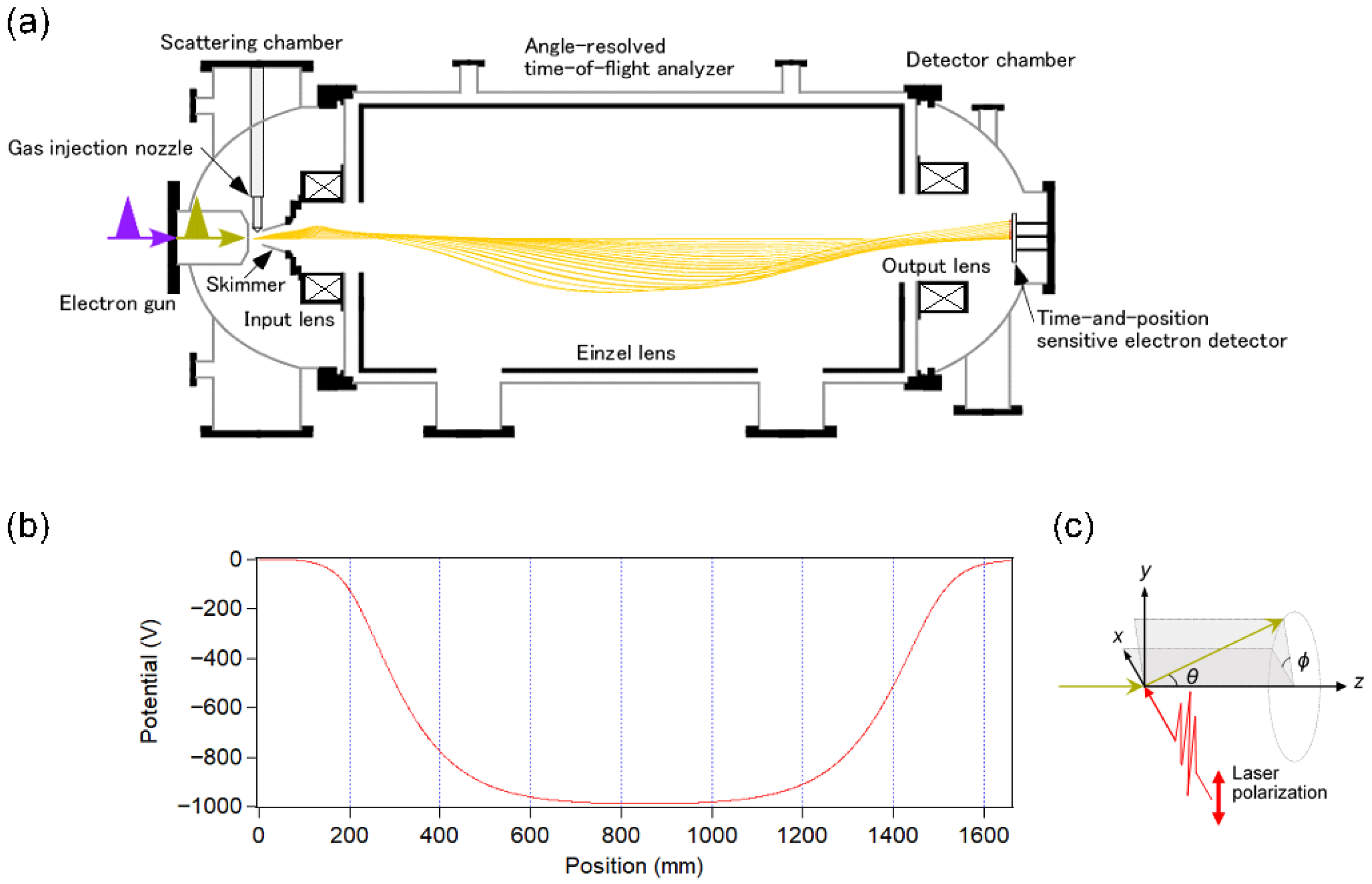
2. Apparatus
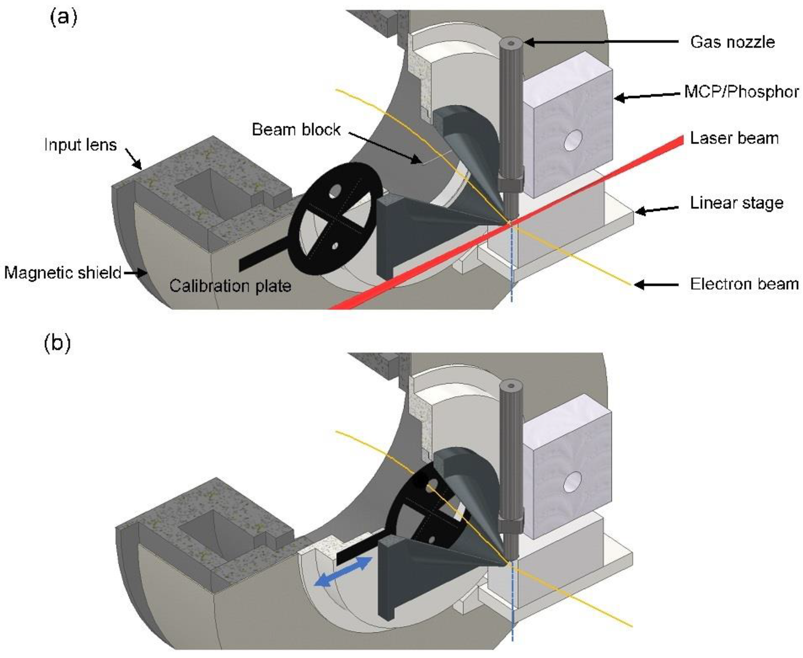
2.1. Vacuum Chambers
2.2. Laser Beam
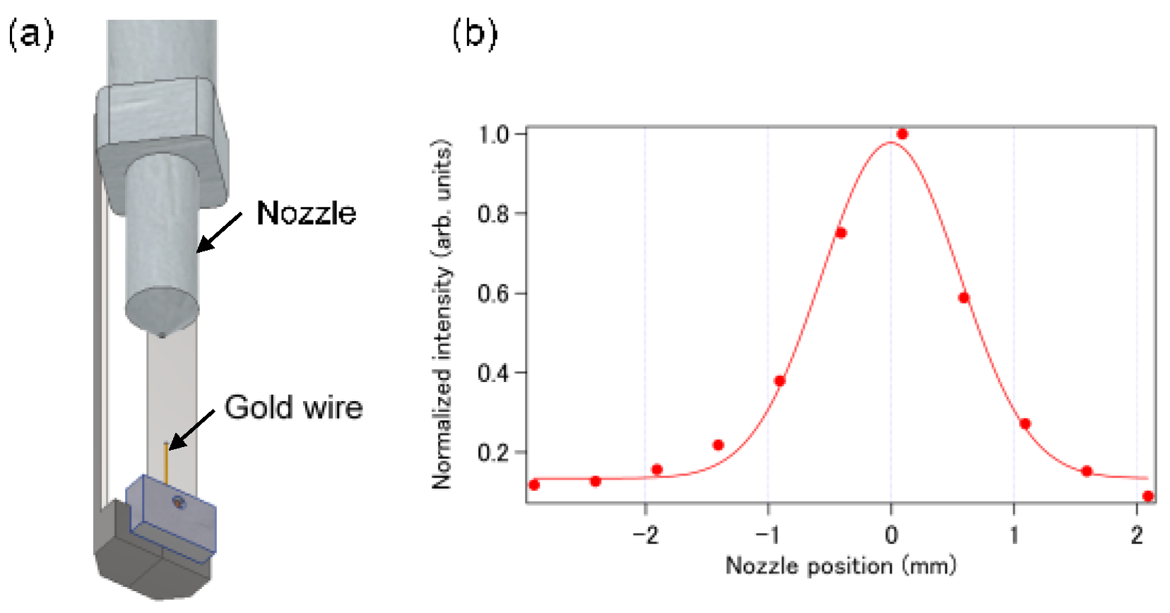
2.3. Sample Gas Beam
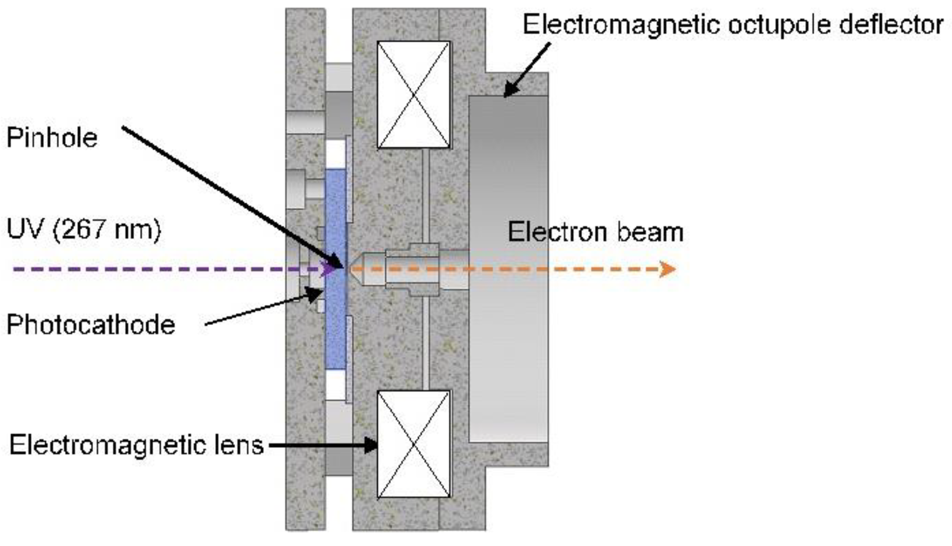
2.4. Electron Beam
2.5. Electron Energy Analyzer and Detector
3. Data Analysis
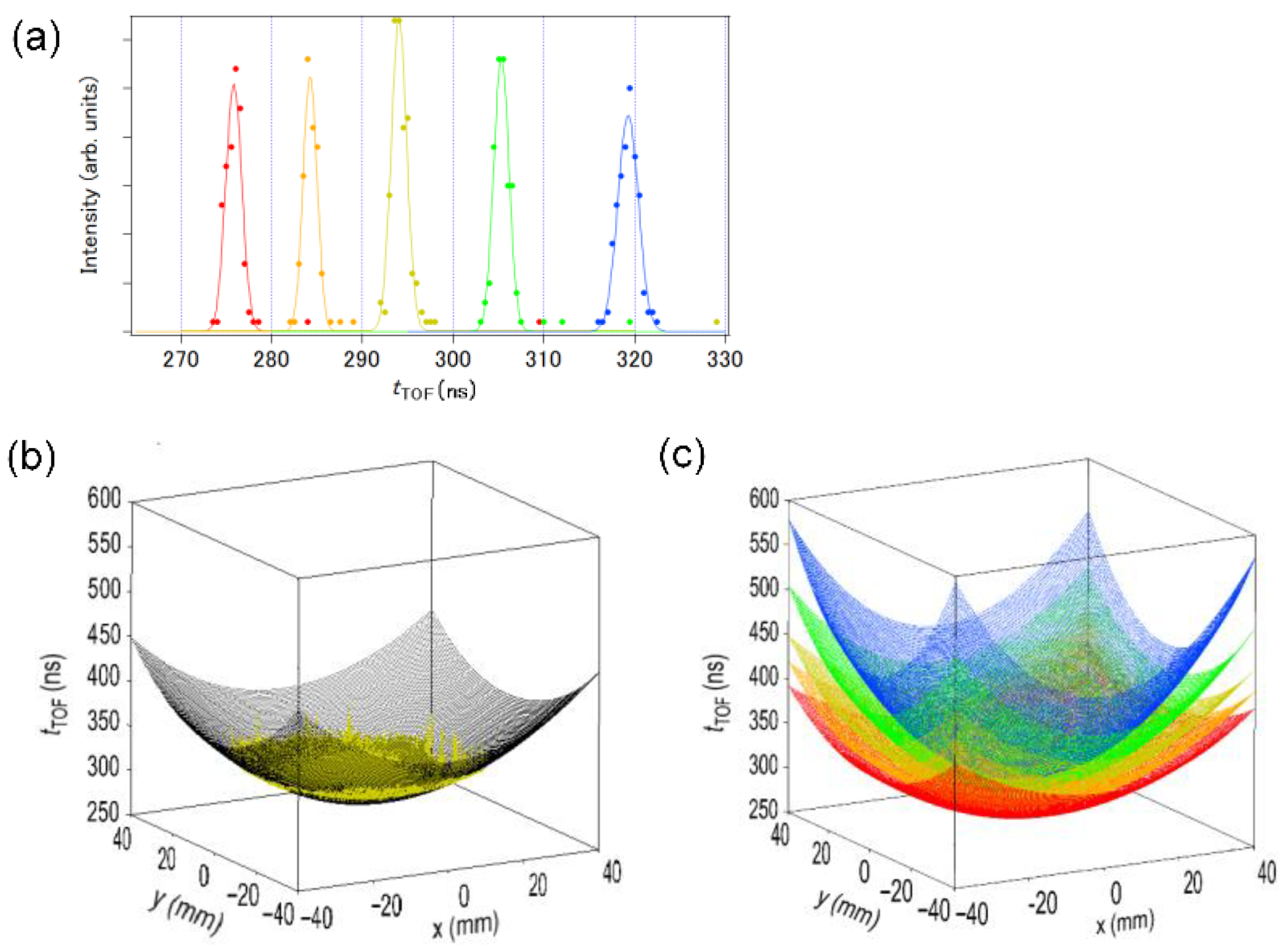
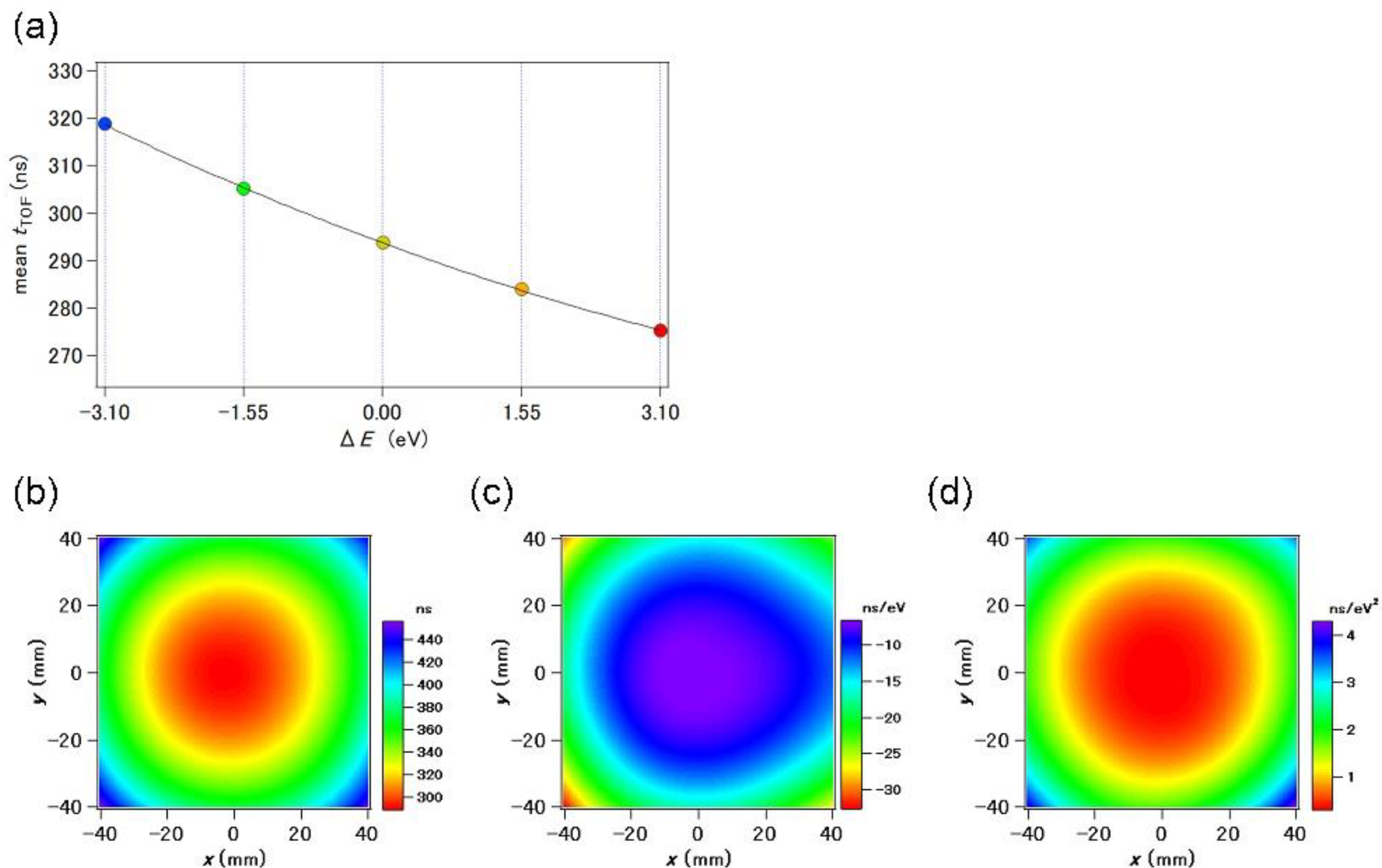
3.1. Determination of ΔE
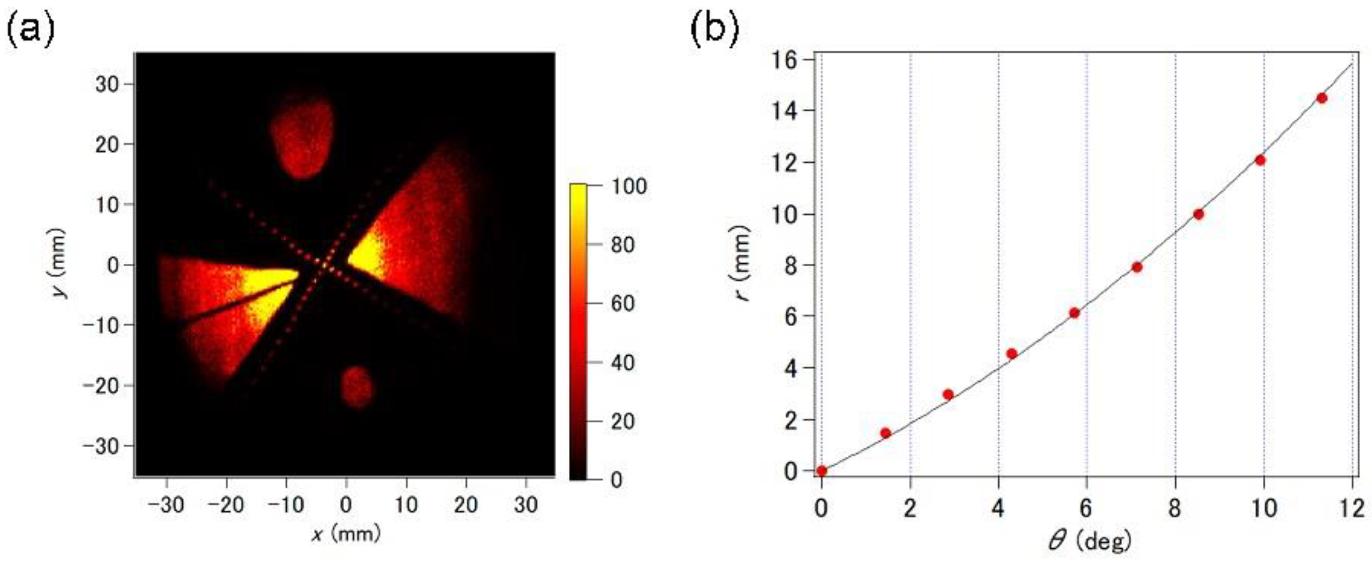
3.2. Determination of θ and ϕ
3.3. Correction of Inhomogeneity of the Detector Sensitivity
4. Performance of Home-Built Apparatus
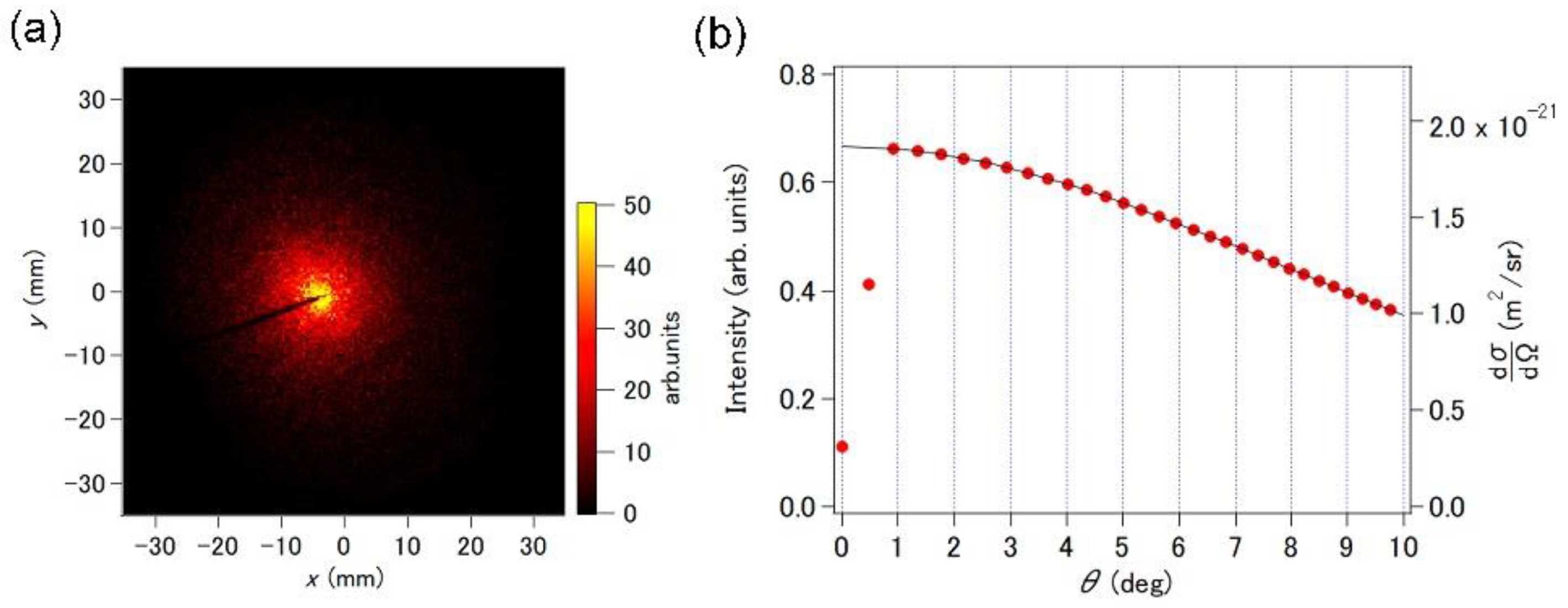
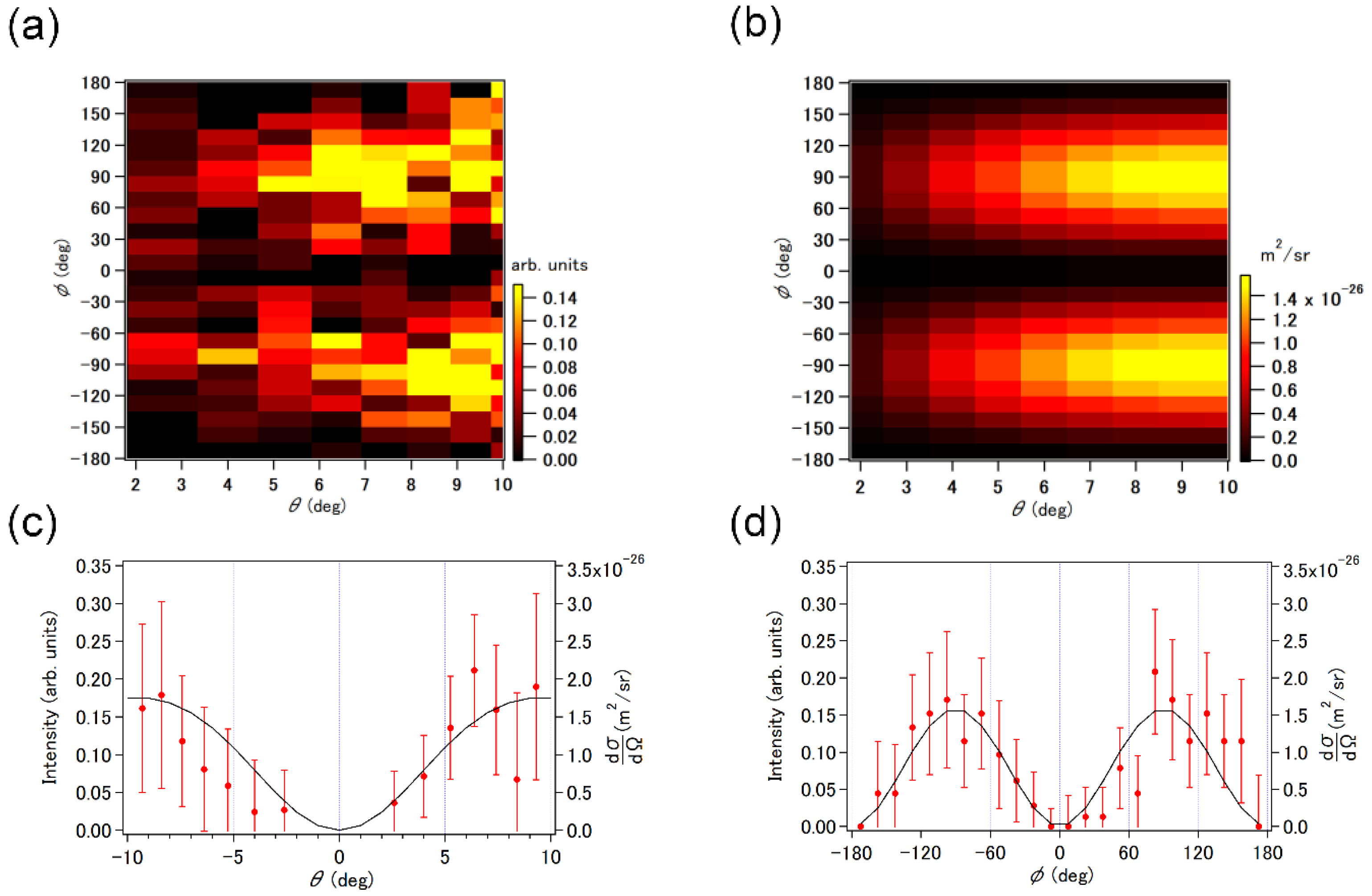
4.1. Angular Distribution of the Scattered Electrons
4.2. Signal Count Rate
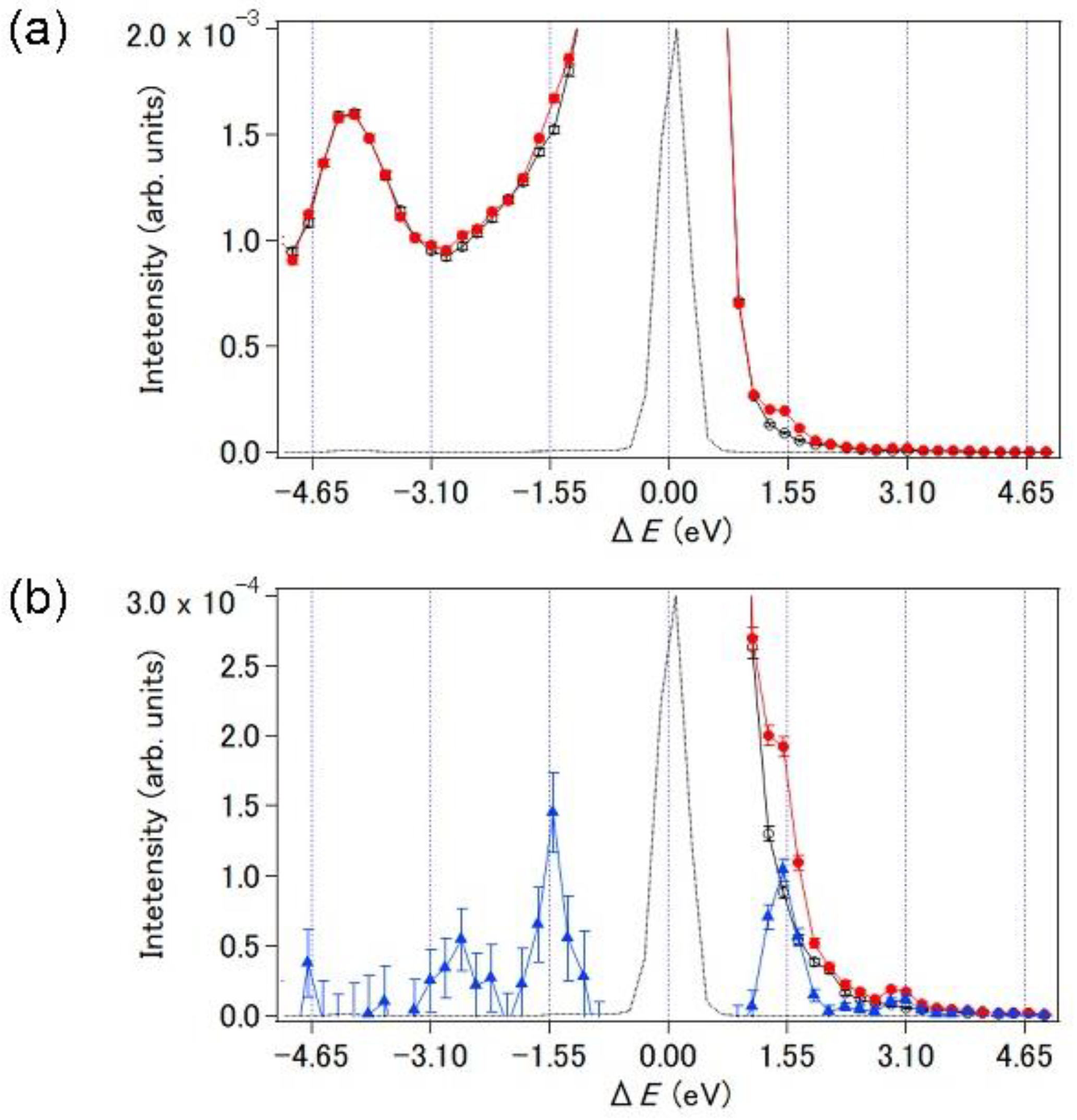
4.3. Kinetic Energy Spectra and LAES Signals
4.4. Two-Dimensional Angular Distribution
5. Summary
Author Contributions
Funding
Institutional Review Board Statement
Informed Consent Statement
Data Availability Statement
Conflicts of Interest
References
- Bunkin, F.V.; Fedorov, M. Bremsstrahlung in a strong radiation field. Sov. Phys. JETP 1966, 22, 844. [Google Scholar]
- Mason, N.J. Laser-assisted electron-atom collisions. Rep. Prog. Phys. 1993, 56, 1275–1346. [Google Scholar] [CrossRef]
- Weingartshofer, A.; Jung, C. Multiphoton free-free transitions. In Multiphoton Ionization of Atoms; Chin, S.L., Ed.; Academic Press: Toronto, ON, Canada, 1984; pp. 155–187. [Google Scholar]
- Ehlotzky, F.; Jaroń, A.; Kamiński, J. Electron–atom collisions in a laser field. Phys. Rep. 1998, 297, 63–153. [Google Scholar] [CrossRef]
- Andrick, D.; Langhans, L. Measurement of free-free transitions in e-Ar scattering. J. Phys. B At. Mol. Phys. 1976, 9, L459–L461. [Google Scholar] [CrossRef]
- Langhans, L. Resonance structures in the free-free cross section of e-Ar scattering. J. Phys. B At. Mol. Phys. 1978, 11, 2361–2366. [Google Scholar] [CrossRef]
- Andrick, D.; Bader, H. Resonance structures in the cross section for free-free radiative transitions in e-He scattering. J. Phys. B At. Mol. Phys. 1984, 17, 4549–4555. [Google Scholar] [CrossRef]
- Bader, H. Resonance structures in the cross section for free-free radiative transitions in e-Ne and e-Ar scattering. J. Phys. B At. Mol. Phys. 1986, 19, 2177–2188. [Google Scholar] [CrossRef]
- Weingartshofer, A.; Holmes, J.K.; Caudle, G.; Clarke, E.M.; Krüger, H. Direct Observation of Multiphoton processes in Laser-Induced Free-Free Transitions. Phys. Rev. Lett. 1977, 39, 269–270. [Google Scholar] [CrossRef]
- Wallbank, B.; Holmes, J.K.; MacIsaac, S.C.; Weingartshofer, A. Resonance structures in free-free cross sections for electron-helium scattering. J. Phys. B At. Mol. Opt. Phys. 1992, 25, 1265–1277. [Google Scholar] [CrossRef]
- Wallbank, B.; Holmes, J.K. Laser-assisted elastic electron-atom collisions. Phys. Rev. A 1993, 48, R2515–R2518. [Google Scholar] [CrossRef]
- Wallbank, B.; Holmes, J.K. Laser-assisted elastic electron scattering from helium. Can. J. Phys. 2001, 79, 1237–1246. [Google Scholar] [CrossRef]
- Nehari, D.; Holmes, J.; Dunseath, K.M.; Terao-Dunseath, M. Experimental and theoretical study of free–free electron–helium scattering in a CO2 laser field. J. Phys. B At. Mol. Opt. Phys. 2010, 43, 25203. [Google Scholar] [CrossRef] [Green Version]
- Wallbank, B.; Holmes, J.K.; Weingartshofer, A. Experimental differential cross sections for multiphoton free-free transitions. J. Phys. B At. Mol. Phys. 1987, 20, 6121–6138. [Google Scholar] [CrossRef]
- Wallbank, B.; Holmes, J.K. Differential cross sections for laser-assisted elastic electron scattering from argon. J. Phys. B At. Mol. Opt. Phys. 1994, 27, 5405–5418. [Google Scholar] [CrossRef]
- Kroll, N.M.; Watson, K.M. Charged-Particle Scattering in the Presence of a Strong Electromagnetic Wave. Phys. Rev. A 1973, 8, 804–809. [Google Scholar] [CrossRef] [Green Version]
- Kanya, R.; Morimoto, Y.; Yamanouchi, K. Observation of Laser-Assisted Electron-Atom Scattering in Femtosecond Intense Laser Fields. Phys. Rev. Lett. 2010, 105, 123202. [Google Scholar] [CrossRef]
- Kanya, R.; Morimoto, Y.; Yamanouchi, K. Apparatus for laser-assisted electron scattering in femtosecond intense laser fields. Rev. Sci. Instrum. 2011, 82, 123105. [Google Scholar] [CrossRef] [PubMed]
- Byron, F.W., Jr.; Joachain, C.J. Electron-atom collisions in a strong laser field. J. Phys. B At. Mol. Phys. 1984, 17, L295–L301. [Google Scholar] [CrossRef]
- Morimoto, Y.; Kanya, R.; Yamanouchi, K. Light-Dressing Effect in Laser-Assisted Elastic Electron Scattering by Xe. Phys. Rev. Lett. 2015, 115, 123201. [Google Scholar] [CrossRef] [Green Version]
- Morimoto, Y.; Kanya, R.; Yamanouchi, K. Laser-assisted electron diffraction for femtosecond molecular imaging. J. Chem. Phys. 2014, 140, 64201. [Google Scholar] [CrossRef]
- Kanya, R.; Yamanouchi, K. Femtosecond Laser-Assisted Electron Scattering for Ultrafast Dynamics of Atoms and Molecules. Atoms 2019, 7, 85. [Google Scholar] [CrossRef]
- Ishida, K.; Morimoto, Y.; Kanya, R.; Yamanouchi, K. High-order multiphoton laser-assisted elastic electron scattering by Xe in a femtosecond near-infrared intense laser field: Plateau in energy spectra of scattered electrons. Phys. Rev. A 2017, 95, 023414. [Google Scholar] [CrossRef]
- Ishida, K. Development of an Apparatus for Femtosecond Laser-Assisted Elastic Electron Scattering with High-Sensitivity and the Observation of High-Order Multiphoton Processes. Doctoral Thesis, The University of Tokyo, Tokyo, Japan, 2017. [Google Scholar] [CrossRef]
- Park, H.; Hao, Z.; Wang, X.; Nie, S.; Clinite, R.; Cao, J. Synchronization of femtosecond laser and electron pulses with subpicosecond precision. Review of scientific instruments. Rev. Sci. Instrum. 2005, 76, 083905. [Google Scholar] [CrossRef] [Green Version]
- Jablonski, A.; Salvat, F.; Powell, C.J. NIST Electron Elastic-Scattering Cross-Section Database-Version 4.0. Natl. Inst. Stand. Technol. 2002. [Google Scholar] [CrossRef]


Disclaimer/Publisher’s Note: The statements, opinions and data contained in all publications are solely those of the individual author(s) and contributor(s) and not of MDPI and/or the editor(s). MDPI and/or the editor(s) disclaim responsibility for any injury to people or property resulting from any ideas, methods, instructions or products referred to in the content. |
© 2023 by the authors. Licensee MDPI, Basel, Switzerland. This article is an open access article distributed under the terms and conditions of the Creative Commons Attribution (CC BY) license (https://creativecommons.org/licenses/by/4.0/).
Share and Cite
Ishikawa, M.; Ishida, K.; Kanya, R.; Yamanouchi, K. Angle-Resolved Time-of-Flight Electron Spectrometer Designed for Femtosecond Laser-Assisted Electron Scattering and Diffraction. Instruments 2023, 7, 4. https://doi.org/10.3390/instruments7010004
Ishikawa M, Ishida K, Kanya R, Yamanouchi K. Angle-Resolved Time-of-Flight Electron Spectrometer Designed for Femtosecond Laser-Assisted Electron Scattering and Diffraction. Instruments. 2023; 7(1):4. https://doi.org/10.3390/instruments7010004
Chicago/Turabian StyleIshikawa, Motoki, Kakuta Ishida, Reika Kanya, and Kaoru Yamanouchi. 2023. "Angle-Resolved Time-of-Flight Electron Spectrometer Designed for Femtosecond Laser-Assisted Electron Scattering and Diffraction" Instruments 7, no. 1: 4. https://doi.org/10.3390/instruments7010004