

Investigating the Intrinsic Anisotropy of VO2(101) Thin Films Using Linearly Polarized Resonant Photoemission Spectroscopy
 , , , and
Abstract
:1. Introduction
2. Experimental
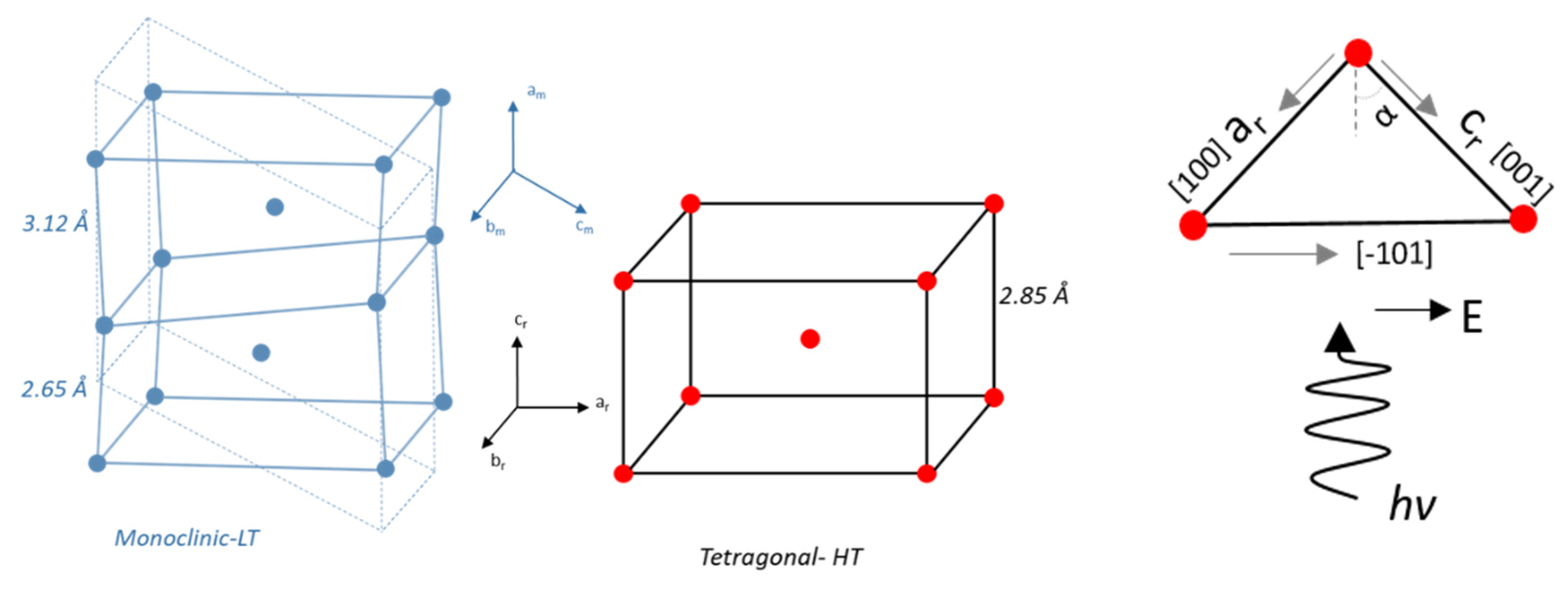
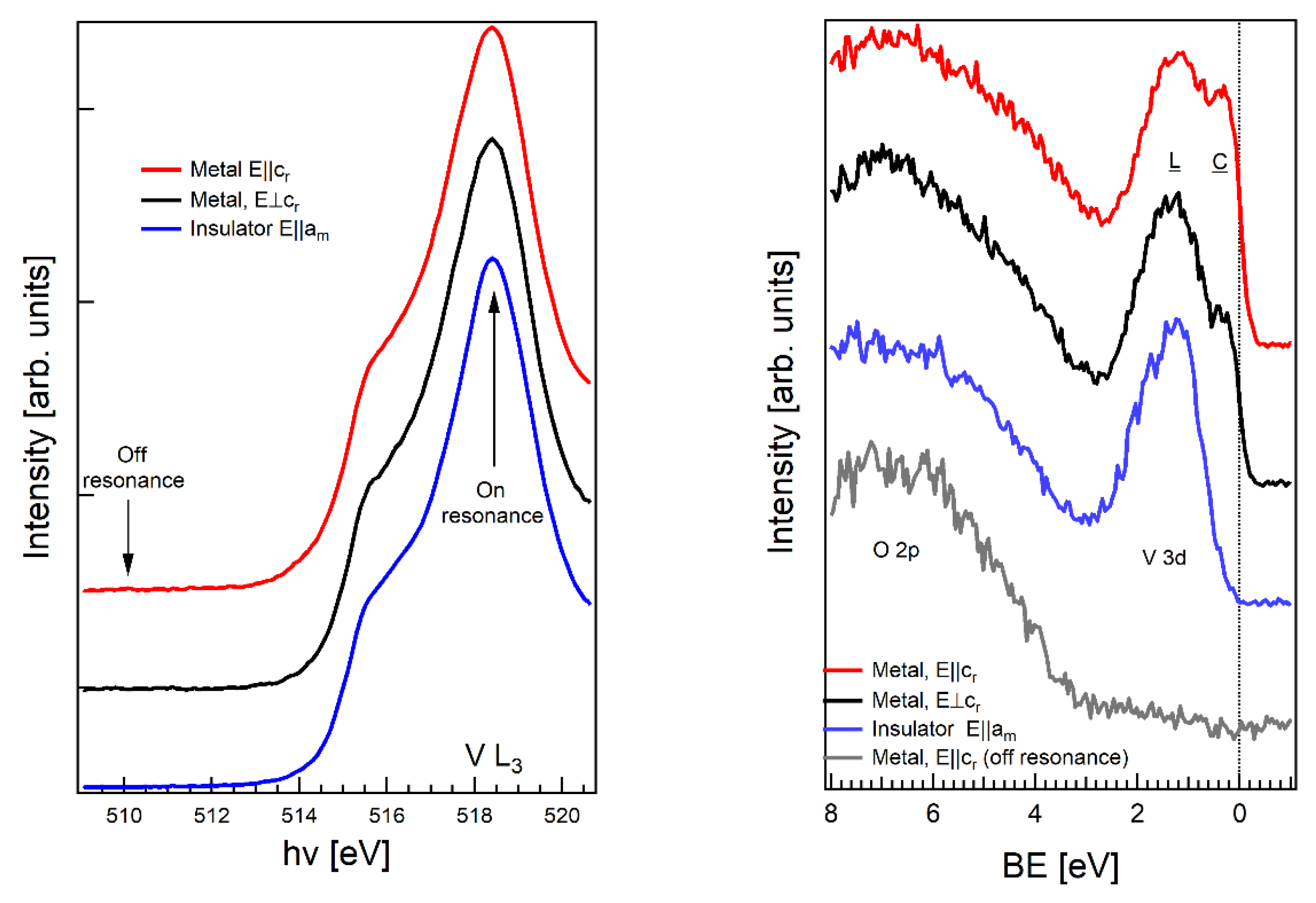
3. Results and Discussion
4. Conclusions
Author Contributions
Funding
Data Availability Statement
Conflicts of Interest
Appendix A
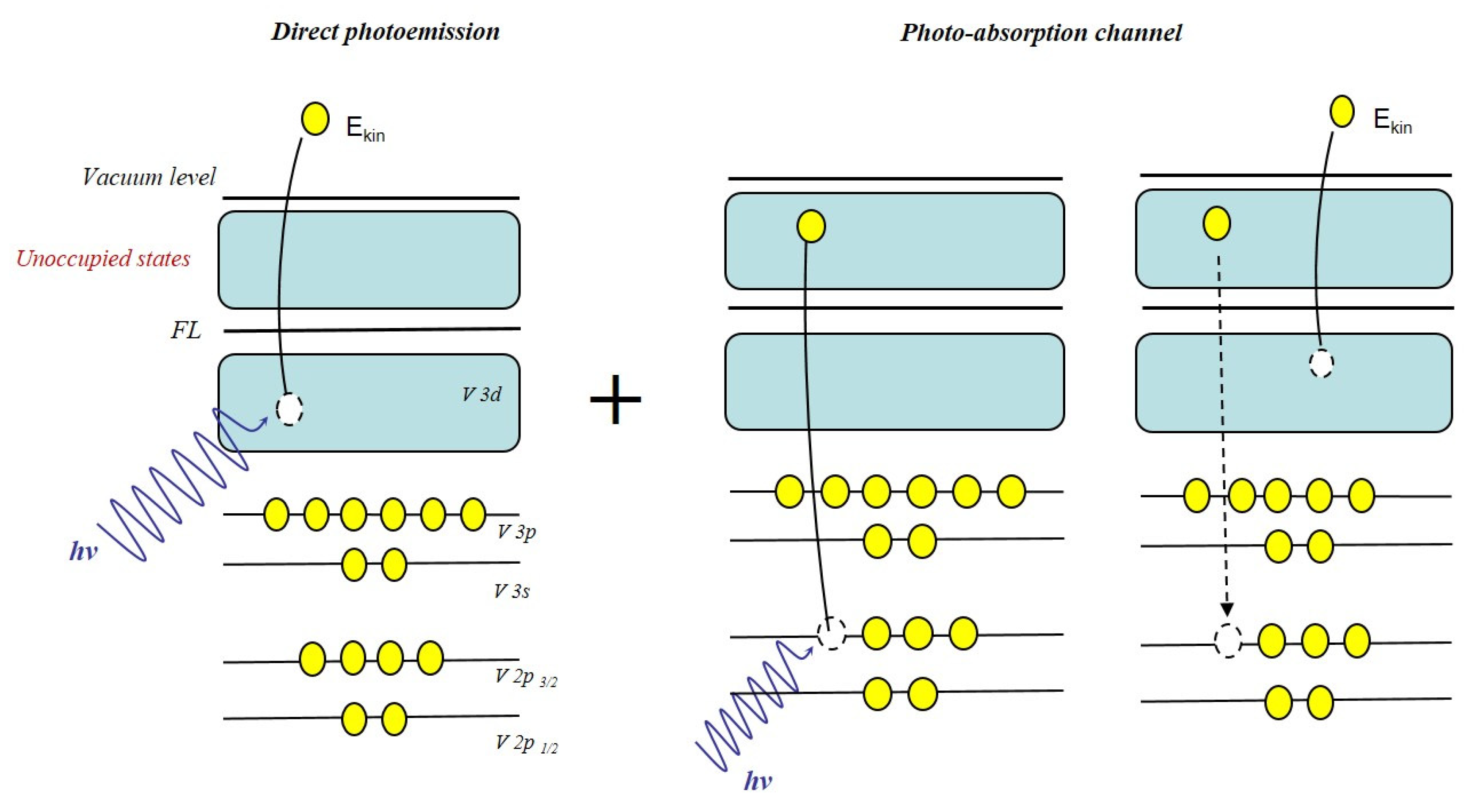
Resonant Photoemission

References
- Fisher, B.; Genossar, J.; Reisner, G. Systematics in the metal-insulator transition temperatures in vanadium oxides. Solid State Commun. 2016, 226, 29–32. [Google Scholar] [CrossRef]
- Eyert, V. The metal-insulator transitions of VO2: A band theoretical approach. Ann. Phys. 2002, 11, 650–704. [Google Scholar] [CrossRef]
- Demeter, M.; Neumann, M.; Reichelt, W. Mixed-valence vanadium oxides studied by XPS. Surf. Sci. 2000, 454, 41–44. [Google Scholar] [CrossRef]
- Shin, S.; Suga, S.; Taniguchi, M.; Fujisawa, M.; Kanzaki, H.; Fujimori, A.; Daimon, H.; Ueda, Y.; Kosuge, K.; Kachi, S. Vacuum-ultraviolet reflectance and photoemission study of the metal-insulator phase transitions in VO2, V6O13, and V2O3. Phys. Rev. B 1990, 41, 4993–5009. [Google Scholar] [CrossRef]
- Haverkort, M.W.; Hu, Z.; Tanaka, A.; Reichelt, W.; Streltsov, S.V.; Korotin, M.A.; Anisimov, V.I.; Hsieh, H.H.; Lin, H.-J.; Chen, C.T.; et al. Orbital-Assisted Metal-Insulator Transition in VO2. Phys. Rev. Lett. 2005, 95, 196404. [Google Scholar] [CrossRef]
- Polewczyk, V.; Chaluvadi, S.; Dagur, D.; Mazzola, F.; Chalil, S.P.; Petrov, A.; Fujii, J.; Panaccione, G.; Rossi, G.; Orgiani, P.; et al. Chemical, structural and electronic properties of ultrathin V2O3 films on Al2O3 substrate: Implications in Mott-like transitions. Appl. Surf. Sci. 2023, 610, 155462. [Google Scholar] [CrossRef]
- D’Elia, A.; Rezvani, S.J.; Zema, N.; Zuccaro, F.; Fanetti, M.; Belec, B.; Li, B.W.; Zou, C.W.; Spezzani, C.; Sacchi, M.; et al. Stoichiometry and disorder influence over electronic structure in nanostructured VOx films. J. Nanoparticle Res. 2021, 23, 33. [Google Scholar] [CrossRef]
- Fu, D.; Liu, K.; Tao, T.; Lo, K.; Cheng, C.; Liu, B.; Zhang, R.; Bechtel, H.A.; Wu, J. Comprehensive study of the metal-insulator transition in pulsed laser deposited epitaxial VO2 thin films. J. Appl. Phys. 2013, 113, 043707. [Google Scholar] [CrossRef]
- Fan, L.L.; Chen, S.; Luo, Z.L.; Liu, Q.H.; Wu, Y.F.; Song, L.; Ji, D.X.; Wang, P.; Chu, W.S.; Gao, C.; et al. Strain Dynamics of Ultrathin VO2 Film Grown on TiO2 (001) and the Associated Phase Transition Modulation. Nano Lett. 2014, 14, 4036–4043. [Google Scholar] [CrossRef]
- Cui, Y.; Ke, Y.; Liu, C.; Chen, Z.; Wang, N.; Zhang, L.; Zhou, Y.; Wang, S.; Gao, Y.; Long, Y. Thermochromic VO2 for Energy-Efficient Smart Windows. Joule 2018, 2, 1707–1746. [Google Scholar] [CrossRef]
- Chen, S.; Wang, Z.; Ren, H.; Chen, Y.; Yan, W.; Wang, C.; Li, B.; Jiang, J.; Zou, C. Gate-controlled VO2 phase transition for high-performance smart windows. Sci. Adv. 2019, 5, eaav6815. [Google Scholar] [CrossRef]
- Kang, C.; Zhang, C.; Yao, Y.; Yang, Y.; Zong, H.; Zhang, L.; Li, M. Enhanced Thermochromic Properties of Vanadium Dioxide (VO2)/Glass Heterostructure by Inserting a Zr-Based Thin Film Metallic Glasses (Cu50Zr50) Buffer Layer. Appl. Sci. 2018, 8, 1751. [Google Scholar] [CrossRef]
- Lin, J.; Ramanathan, S.; Guha, S. Electrically Driven Insulator–Metal Transition-Based Devices—Part I: The Electrothermal Model and Experimental Analysis for the DC Characteristics. IEEE Trans. Electron. Devices 2018, 65, 3982–3988. [Google Scholar] [CrossRef]
- Ramanathan, S. Thin Film Metal-Oxides: Fundamentals and Applications in Electronics and Energy; Springer: Boston, MA, USA, 2010. [Google Scholar] [CrossRef]
- Brahlek, M.; Zhang, L.; Lapano, J.; Zhang, H.-T.; Engel-Herbert, R.; Shukla, N.; Datta, S.; Paik, H.; Schlom, D.G. Opportunities in vanadium-based strongly correlated electron systems. MRS Commun. 2017, 7, 27–52. [Google Scholar] [CrossRef]
- Zimmermann, R.; Claessen, R.; Reinert, F.; Steiner, P.; Hüfner, S. Strong hybridization in vanadium oxides: Evidence from photoemission and absorption spectroscopy. J. Phys. Condens. Matter 1998, 10, 5697–5716. [Google Scholar] [CrossRef]
- Qazilbash, M.M.; Burch, K.; Whisler, D.; Shrekenhamer, D.; Chae, B.G.; Kim, H.T.; Basov, D.N. Correlated metallic state of vanadium dioxide. Phys. Rev. B Condens. Matter Mater. Phys. 2006, 74, 205118. [Google Scholar] [CrossRef]
- Weber, C.; O’regan, D.D.; Hine, N.D.M.; Payne, M.C.; Kotliar, G.; Littlewood, P.B. Vanadium Dioxide: A Peierls-Mott Insulator Stable against Disorder. Phys. Rev. Lett. 2012, 108, 256402. [Google Scholar] [CrossRef]
- Zylbersztejn, A.; Mott, N.F. Metal-insulator transition in vanadium dioxide. Phys. Rev. B 1975, 11, 4383–4395. [Google Scholar] [CrossRef]
- Koethe, T.C.; Hu, Z.; Haverkort, M.W.; Schüßler-Langeheine, C.; Venturini, F.; Brookes, N.B.; Tjernberg, O.; Reichelt, W.; Hsieh, H.H.; Lin, H.-J.; et al. Transfer of Spectral Weight and Symmetry across the Metal-Insulator Transition in VO2. Phys. Rev. Lett. 2006, 97, 116402. [Google Scholar] [CrossRef]
- D’Elia, A.; Grazioli, C.; Cossaro, A.; Li, B.W.; Zou, C.W.; Rezvani, S.J.; Pinto, N.; Marcelli, A.; Coreno, M. Electron Correlation driven Metal-Insulator transition in Strained and Disordered VO2 films. arXiv 2020, arXiv:2006.07930. [Google Scholar]
- Singh, C.N.; Piper, L.F.J.; Paik, H.; Schlom, D.G.; Lee, W.-C. Correlation-induced emergent charge order in metallic vanadium dioxide. arXiv 2020, arXiv:2005.02957. [Google Scholar] [CrossRef]
- Aetukuri, N.B.; Gray, A.X.; Drouard, M.; Cossale, M.; Gao, L.; Reid, A.H.; Kukreja, R.; Ohldag, H.; Jenkins, C.A.; Arenholz, E.; et al. Control of the metal–insulator transition in vanadium dioxide by modifying orbital occupancy. Nat. Phys. 2013, 9, 661–666. [Google Scholar] [CrossRef]
- Natelson, D. Condensed-matter physics: A solid triple point. Nature 2013, 500, 408–409. [Google Scholar] [CrossRef] [PubMed]
- Tricoire, M.; Mahieu, N.; Simler, T.; Nocton, G. Intermediate Valence States in Lanthanide Compounds. Chem. A Eur. J. 2021, 27, 6860–6879. [Google Scholar] [CrossRef] [PubMed]
- Pruessmann, T.; Nagel, P.; Simonelli, L.; Batchelor, D.; Gordon, R.; Schimmelpfennig, B.; Trumm, M.; Vitova, T. Opportunities and challenges of applying advanced X-ray spectroscopy to actinide and lanthanide N-donor ligand systems. J. Synchrotron. Radiat. 2022, 29, 53–66. [Google Scholar] [CrossRef] [PubMed]
- Bianconi, A.; Marcelli, A.; Dexpert, H.; Karnatak, R.; Kotani, A.; Jo, T.; Petiau, J. Specific intermediate-valence state of insulating 4f compounds detected by L3 X-ray absorption. Phys. Rev. B 1987, 35, 806–812. [Google Scholar] [CrossRef]
- Bianconi, A. Multiplet splitting of final-state configurations in X-ray-absorption spectrum of metal VO2: Effect of core-hole-screening, electron correlation, and metal-insulator transition. Phys. Rev. B 1982, 26, 2741–2747. [Google Scholar] [CrossRef]
- Gray, A.X.; Jeong, J.; Aetukuri, N.P.; Granitzka, P.; Chen, Z.; Kukreja, R.; Higley, D.; Chase, T.; Reid, A.H.; Ohldag, H.; et al. Correlation-Driven Insulator-Metal Transition in Near-Ideal Vanadium Dioxide Films. Phys. Rev. Lett. 2016, 116, 116403. [Google Scholar] [CrossRef]
- Paez, G.J.; Singh, C.N.; Wahila, M.J.; Tirpak, K.E.; Quackenbush, N.F.; Sallis, S.; Paik, H.; Liang, Y.; Schlom, D.G.; Lee, T.-L.; et al. Simultaneous Structural and Electronic Transitions in Epitaxial VO2/TiO2(001). Phys. Rev. Lett. 2020, 124, 196402. [Google Scholar] [CrossRef]
- Mukherjee, S.; Quackenbush, N.F.; Paik, H.; Schlueter, C.; Lee, T.-L.; Schlom, D.G.; Piper, L.F.J.; Lee, W.-C. Tuning a strain-induced orbital selective Mott transition in epitaxial VO2. Phys. Rev. B 2016, 93, 241110. [Google Scholar] [CrossRef]
- Evlyukhin, E.; Howard, S.A.; Paik, H.; Paez, G.J.; Gosztola, D.J.; Singh, C.N.; Schlom, D.G.; Lee, W.-C.; Piper, L.F.J. Directly measuring the structural transition pathways of strain-engineered VO2 thin films. Nanoscale 2020, 12, 18857–18863. [Google Scholar] [CrossRef]
- D’Elia, A.; Grazioli, C.; Cossaro, A.; Li, B.; Zou, C.; Rezvani, S.J.; Marcelli, A.; Coreno, M. Detection of Spin Polarized Band in VO2/TiO2(001) Strained Films via Orbital Selective Constant Initial State Spectroscopy. Condens. Matter 2020, 5, 72. [Google Scholar] [CrossRef]
- D’Elia, A.; Rezvani, S.; Cossaro, A.; Stredansky, M.; Grazioli, C.; Li, B.W.; Zou, C.; Coreno, M.; Marcelli, A. Strain Induced Orbital Dynamics Across the Metal Insulator Transition in Thin VO2/TiO2 (001) Films. J. Supercond. Nov. Magn. 2020, 33, 2383–2388. [Google Scholar] [CrossRef]
- Mondal, D.; Mahapatra, S.R.; Ahmed, T.; Podapangi, S.K.; Ghosh, A.; Aetukuri, N.P.B. Atomically-smooth single-crystalline VO2 (101) thin films with sharp metal-insulator transition. J. Appl. Phys. 2019, 126, 215302. [Google Scholar] [CrossRef]
- Lu, J.; West, K.G.; Wolf, S.A. Very large anisotropy in the dc conductivity of epitaxial VO2 thin films grown on (011) rutile TiO2 substrates. Appl. Phys. Lett. 2008, 93, 262107. [Google Scholar] [CrossRef]
- Kittiwatanakul, S.; Lu, J.; Wolf, S.A. Transport Anisotropy of Epitaxial VO2 Films near the Metal–Semiconductor Transition. Appl. Phys. Express 2011, 4, 091104. [Google Scholar] [CrossRef]
- Lee, S.; Hippalgaonkar, K.; Yang, F.; Hong, J.; Ko, C.; Suh, J.; Liu, K.; Wang, K.; Urban, J.J.; Zhang, X.; et al. Anomalously low electronic thermal conductivity in metallic vanadium dioxide. Science 2017, 355, 371–374. [Google Scholar] [CrossRef]
- Bongers, P. Anisotropy of the electrical conductivity of VO2 single crystals. Solid State Commun. 1965, 3, 275–277. [Google Scholar] [CrossRef]
- Goodenough, J.B. The two components of the crystallographic transition in VO2. J. Solid State Chem. 1971, 3, 490–500. [Google Scholar] [CrossRef]
- D’Elia, A.; Grazioli, C.; Cossaro, A.; Li, B.; Zou, C.; Rezvani, S.; Pinto, N.; Marcelli, A.; Coreno, M. Strain mediated Filling Control nature of the Metal-Insulator Transition of VO2 and electron correlation effects in nanostructured films. Appl. Surf. Sci. 2020, 540, 148341. [Google Scholar] [CrossRef]
- Fan, L.L.; Chen, S.; Liao, G.M.; Chen, Y.L.; Ren, H.; Zou, C.W. Comprehensive studies of interfacial strain and oxygen vacancy on metal–insulator transition of VO2 film. J. Phys. Condens. Matter 2016, 28, 255002. [Google Scholar] [CrossRef] [PubMed]
- Marcelli, A.; Coreno, M.; Stredansky, M.; Xu, W.; Zou, C.; Fan, L.; Chu, W.; Wei, S.; Cossaro, A.; Ricci, A.; et al. Nanoscale Phase Separation and Lattice Complexity in VO2: The Metal–Insulator Transition Investigated by XANES via Auger Electron Yield at the Vanadium L23-Edge and Resonant Photoemission. Condens. Matter 2017, 2, 38. [Google Scholar] [CrossRef]
- Laverock, J.; Preston, A.R.H.; Newby, J.D.; Smith, K.E.; Sallis, S.; Piper, L.F.J.; Kittiwatanakul, S.; Lu, J.W.; Wolf, S.A.; Leandersson, M.; et al. Photoemission evidence for crossover from Peierls-like to Mott-like transition in highly strained VO2. Phys. Rev. B Condens. Matter Mater. Phys. 2012, 86, 195124. [Google Scholar] [CrossRef]
- Fan, L.L.; Chen, S.; Wu, Y.F.; Chen, F.H.; Chu, W.S.; Chen, X.; Zou, C.W.; Wu, Z.Y. Growth and phase transition characteristics of pure M-phase VO2 epitaxial film prepared by oxide molecular beam epitaxy. Appl. Phys. Lett. 2013, 103, 131914. [Google Scholar] [CrossRef]
- Panaccione, G.; Vobornik, I.; Fujii, J.; Krizmancic, D.; Annese, E.; Giovanelli, L.; Maccherozzi, F.; Salvador, F.; De Luisa, A.; Benedetti, D.; et al. Advanced photoelectric effect experiment beamline at Elettra: A surface science laboratory coupled with Synchrotron Radiation. Rev. Sci. Instrum. 2009, 80, 043105. [Google Scholar] [CrossRef]
- Stöhr, J. Principles, Techniques, and Instrumentation of NEXAFS. NEXAFS Spectrosc. 1992, 25, 114–161. [Google Scholar] [CrossRef]
- Kittiwatanakul, S.; Wolf, S.A.; Lu, J. Large epitaxial bi-axial strain induces a Mott-like phase transition in VO2. Appl. Phys. Lett. 2014, 105, 073112. [Google Scholar] [CrossRef]
- Eguchi, R.; Taguchi, M.; Matsunami, M.; Horiba, K.; Yamamoto, K.; Ishida, Y.; Chainani, A.; Takata, Y.; Yabashi, M.; Miwa, D.; et al. Photoemission evidence for a Mott-Hubbard metal-insulator transition in VO2. Phys. Rev. B Condens. Matter Mater. Phys. 2008, 78, 075115. [Google Scholar] [CrossRef]
- D’Elia, A.; Cepek, C.; de Simone, M.; Macis, S.; Belec, B.; Fanetti, M.; Piseri, P.; Marcelli, A.; Coreno, M. Interplay among work function, electronic structure and stoichiometry in nanostructured VOx films. Phys. Chem. Chem. Phys. 2020, 22, 6282–6290. [Google Scholar] [CrossRef]
- Mossanek, R.J.O.; Abbate, M. Cluster model calculations with nonlocal screening channels of metallic and insulating VO2. Phys. Rev. B Condens. Matter Mater. Phys. 2006, 74, 125112. [Google Scholar] [CrossRef]
- Dowben, P. The metallicity of thin films and overlayers. Surf. Sci. Rep. 2000, 40, 151–247. [Google Scholar] [CrossRef]
- McIlroy, D.N.; Waldfried, C.; Zhang, J.; Choi, J.-W.; Foong, F.; Liou, S.H.; Dowben, P.A. Comparison of the temperature-dependent electronic structure of the perovskites. Phys. Rev. B Condens. Matter Mater. Phys. 1996, 54, 17438–17451. [Google Scholar] [CrossRef]
- Li, D.; Zhang, J.; Lee, S.; Dowben, P.A. Evidence for the formation of metallic mercury overlayers on Si(111). Phys. Rev. B 1992, 45, 11876–11884. [Google Scholar] [CrossRef]
- Tanaka, A.; Jo, T. Resonant 3d, 3p and 3s Photoemission in Transition Metal Oxides Predicted at 2p Threshold. J. Phys. Soc. Jpn. 1994, 63, 2788–2807. [Google Scholar] [CrossRef]


| 0.418 | 0.502 |
Disclaimer/Publisher’s Note: The statements, opinions and data contained in all publications are solely those of the individual author(s) and contributor(s) and not of MDPI and/or the editor(s). MDPI and/or the editor(s) disclaim responsibility for any injury to people or property resulting from any ideas, methods, instructions or products referred to in the content. |
© 2023 by the authors. Licensee MDPI, Basel, Switzerland. This article is an open access article distributed under the terms and conditions of the Creative Commons Attribution (CC BY) license (https://creativecommons.org/licenses/by/4.0/).
Share and Cite
D’Elia, A.; Polewczyk, V.; Petrov, A.Y.; Li, L.; Zou, C.; Rezvani, J.; Marcelli, A. Investigating the Intrinsic Anisotropy of VO2(101) Thin Films Using Linearly Polarized Resonant Photoemission Spectroscopy. Condens. Matter 2023, 8, 40. https://doi.org/10.3390/condmat8020040
D’Elia A, Polewczyk V, Petrov AY, Li L, Zou C, Rezvani J, Marcelli A. Investigating the Intrinsic Anisotropy of VO2(101) Thin Films Using Linearly Polarized Resonant Photoemission Spectroscopy. Condensed Matter. 2023; 8(2):40. https://doi.org/10.3390/condmat8020040
Chicago/Turabian StyleD’Elia, Alessandro, Vincent Polewczyk, Aleksandr Yu. Petrov, Liang Li, Chongwen Zou, Javad Rezvani, and Augusto Marcelli. 2023. "Investigating the Intrinsic Anisotropy of VO2(101) Thin Films Using Linearly Polarized Resonant Photoemission Spectroscopy" Condensed Matter 8, no. 2: 40. https://doi.org/10.3390/condmat8020040