
Detection of Surface States in Quantum Materials ZrTe2 and TmB4 by Scanning Tunneling Microscopy
 , , , and
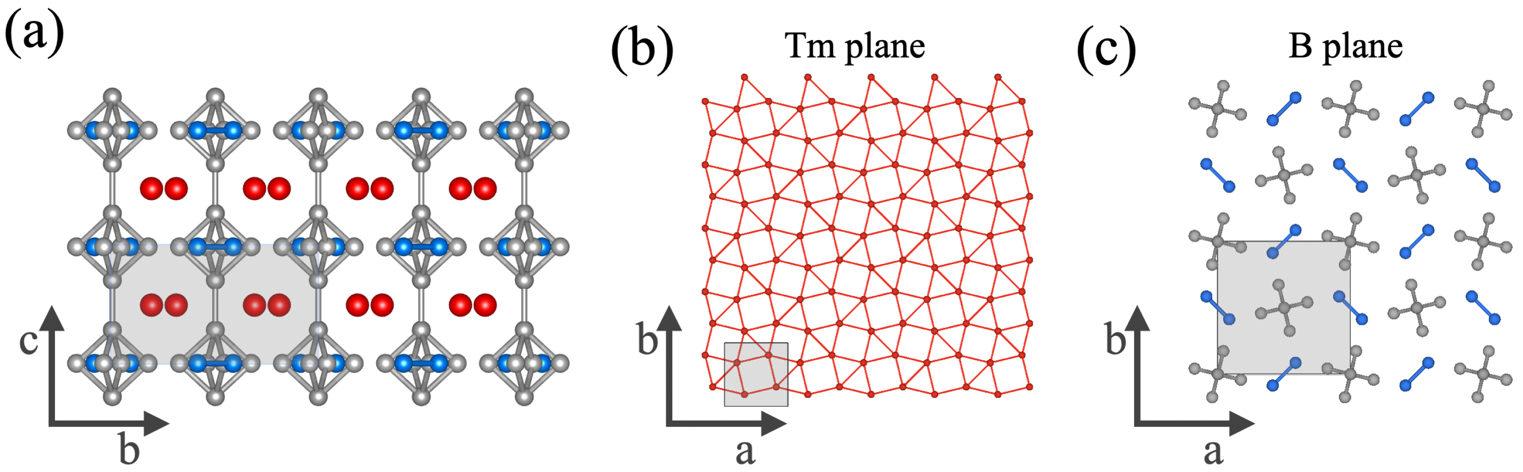
Abstract
:1. Introduction
2. Samples and Experiments
3. Results
3.1. ZrTe2
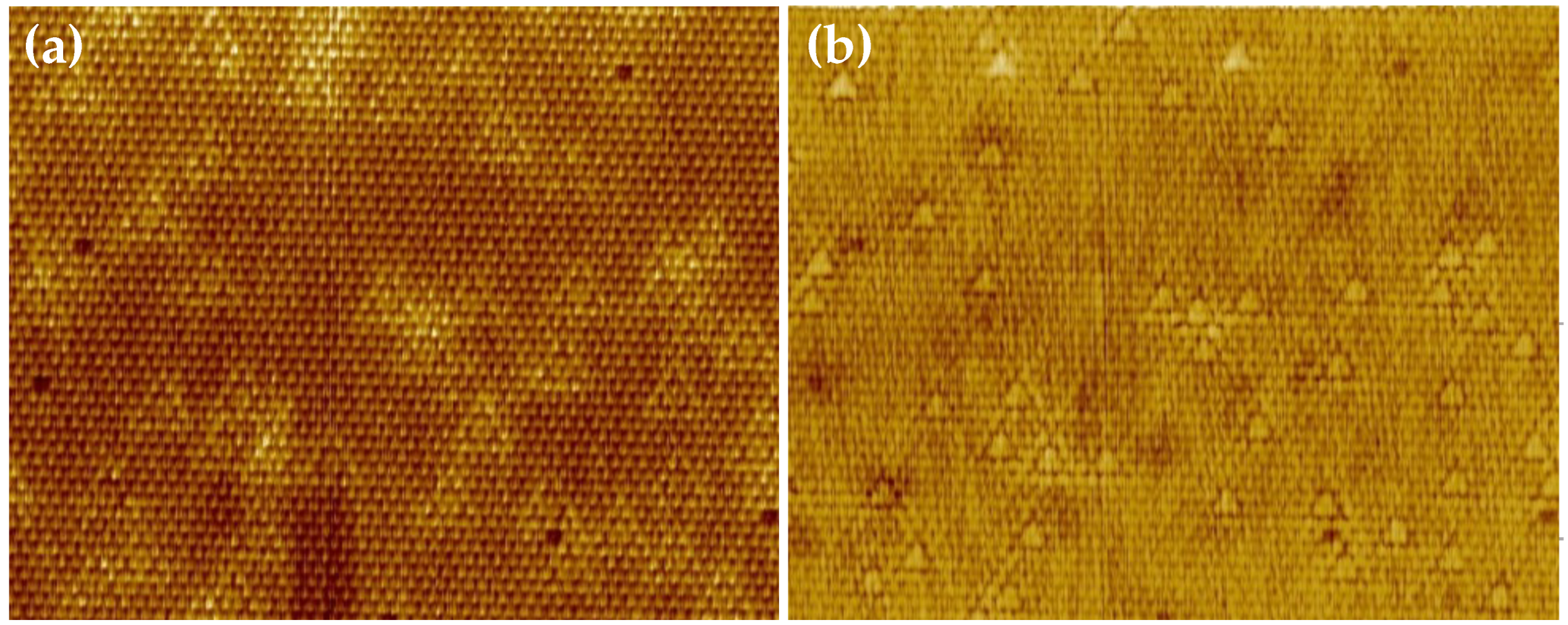
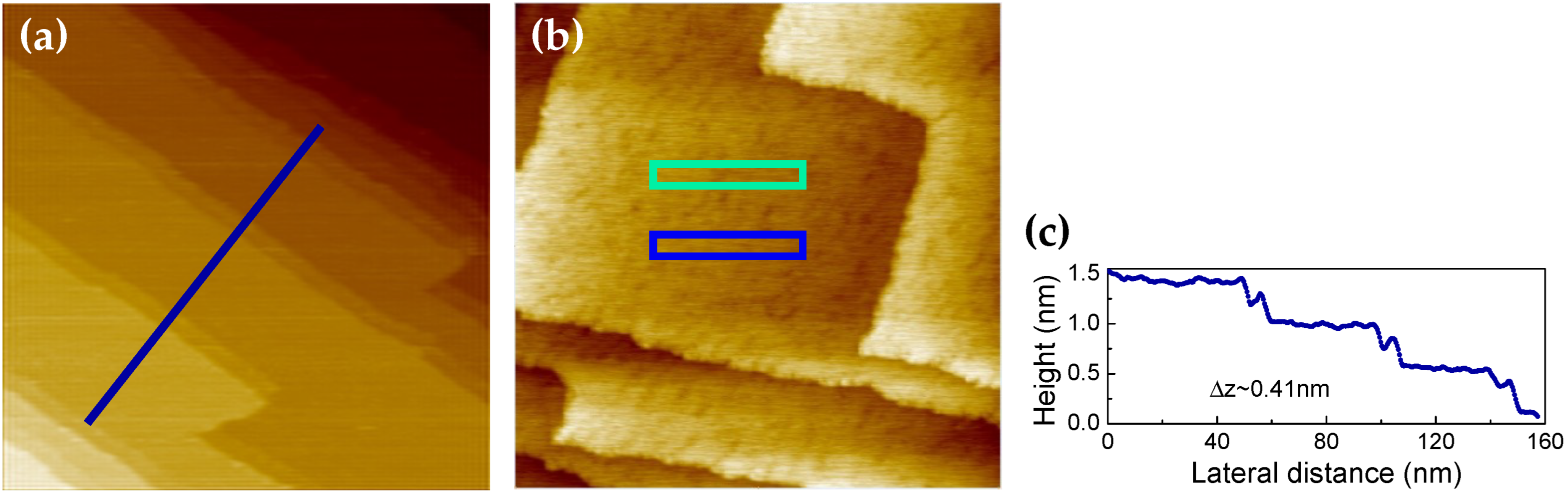
3.1.1. Topography
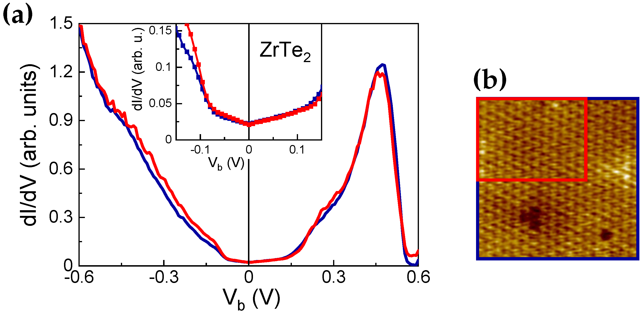
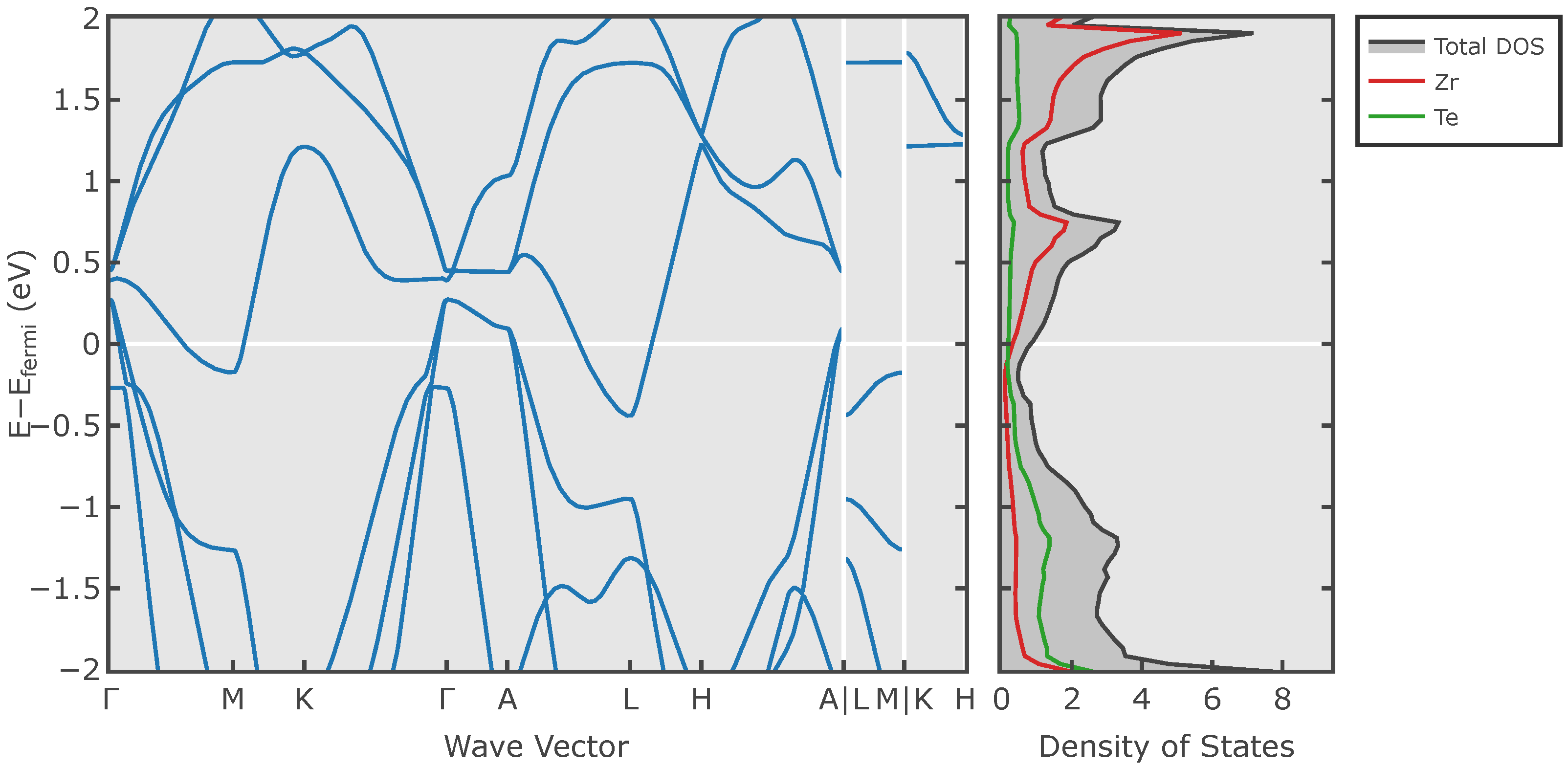
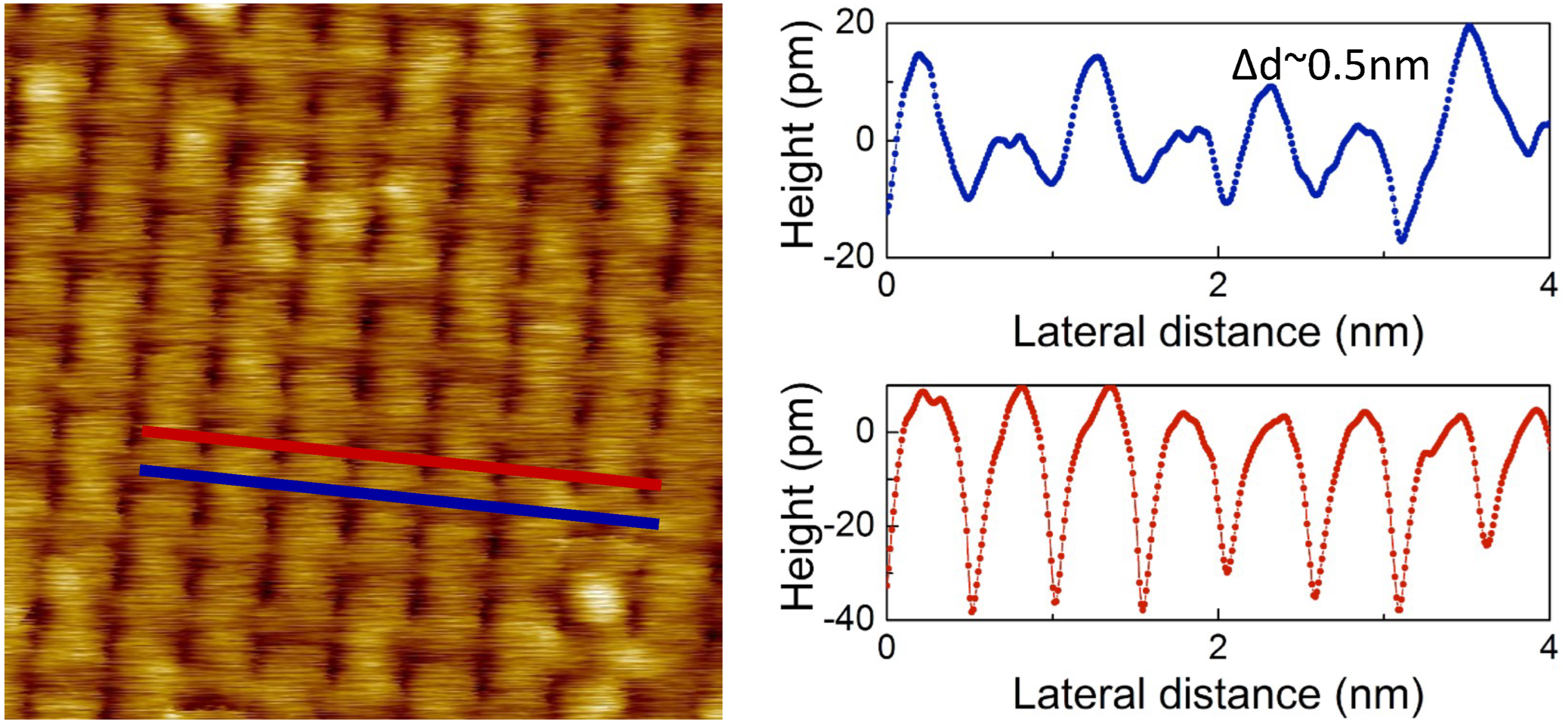
3.1.2. Spectroscopy
3.2. TmB4
3.2.1. Topography
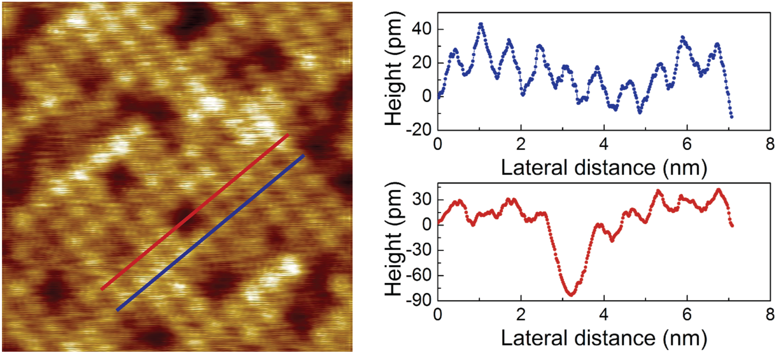
3.2.2. Spectroscopy

4. Discussion
Supplementary Materials
Author Contributions
Funding
Institutional Review Board Statement
Data Availability Statement
Acknowledgments
Conflicts of Interest
References
- Hataugai, Y. Topological aspects of the quantum Hall effect. J. Phys. Condens. Matter 1997, 9, 2507–25491. [Google Scholar] [CrossRef]
- Kane, C.L.; Mele, E.J. Z2 Topological Order and the Quantum Spin Hall Effect. Phys. Rev. Lett. 2005, 95, 146802. [Google Scholar] [CrossRef] [PubMed] [Green Version]
- Bernevig, B.A.; Hughes, T.L.; Zhang, S.C. Quantum spin Hall effect and topological phase transition in HgTe quantum wells. Science 2006, 314, 1757–1761. [Google Scholar] [CrossRef] [PubMed] [Green Version]
- König, M.; Wiedmann, S.; Brüne, C.; Roth, A.; Buhmann, H.; Molenkamp, I.W.; Qi, X.L.; Zhang, S.C. Quantum spin Hall insulator state in HgTe quantum wells. Science 2007, 318, 766–770. [Google Scholar] [CrossRef] [PubMed] [Green Version]
- Fu, L.; Kane, C.L.; Mele, E.J. Topological Insulators in Three Dimensions. Phys. Rev. Lett. 2007, 98, 106803. [Google Scholar] [CrossRef] [PubMed] [Green Version]
- Fu, L.; Kane, C.L. Superconducting proximity effect and Majorana fermions at surface of a topological insulator. Phys. Rev. Lett. 2008, 100, 096407. [Google Scholar] [CrossRef] [Green Version]
- Hasan, H.Z.; Kane, C.L. Colloquium: Topological insulators. Rev. Mod. Phys. 2010, 82, 3045–3067. [Google Scholar] [CrossRef] [Green Version]
- Armitage, N.P.; Mele, E.J.; Vishwanath, A. Weyl and Dirac semimetals in three-dimensional solids. Rev. Mod. Phys. 2018, 90, 015001. [Google Scholar] [CrossRef] [Green Version]
- Wieder, B.J.; Bradlyn, B.; Cano, J.; Nang, Z.; Vergniory, M.G.; Elcoro, L.; Soluyanov, A.A.; Felser, C.; Neu, T.; Regnault, N.; et al. Topological materials discovery from crystal symmetry. Nat. Rev. Mater. 2022, 17, 196–216. [Google Scholar] [CrossRef]
- Lu, D.; Vishik, I.M.; Yi, M.; Moore, R.G.; Shen, Z.X. Angle-resolved photoemission Studies of Quantum Materials. Annu. Rev. Condens. Matter Phys. 2012, 3, 129–167. [Google Scholar] [CrossRef]
- Lv, B.; Qian, T.; Ding, H. Angle-resolved photoemission spectroscopy and its application to topological materials. Nat. Rev. Phys. 2019, 1, 609–626. [Google Scholar] [CrossRef] [Green Version]
- Chen, Y.; Gu, X.; Li, Y.; Du, X.; Yang, L.; Chen, Y. Recent advances in Topological Quantum Materials by angle-resolved Photoemission spectroscopy. Matter 2020, 3, 1114–1141. [Google Scholar] [CrossRef]
- Sobota, J.A.; He, Y.; Shen, Z.X. Topological materials discovery from crystal symmetry. Rev. Mod. Phys. 2021, 93, 025006. [Google Scholar] [CrossRef]
- Rader, O.; Sanchez-Barriga, J.; Rienks, E.D.L.; Varykhalov, A.; Springholz, G.; Yashina, L.V. Angle-resolved photoemission of topological matter: Examples from magnetism, electron correlation, and phase transitions. Phys. Stat. Sol. B 2021, 258, 2000371. [Google Scholar] [CrossRef]
- Hsieh, D.; Xia, Y.; Wray, L.; Qian, D.; Pal, A.; Dil, J.H.; Osterwalder, J.; Meier, F.; Bihlmayer, G.; Kane, C.L.; et al. Observation of unconventional Quantum spin texture in topological insulator. Science 2009, 323, 919–922. [Google Scholar] [CrossRef] [Green Version]
- Xu, N.; Biswas, P.K.; Dil, J.H.; Dhaka, R.S.; Landolt, G.; Muff, S.; Matt, C.E.; Shi, X.; Plumb, N.C.; Radović, M.; et al. Direct observation of the spin texture in SmB6 as evidence of the topological Kondo insulator. Nat. Commun. 2014, 5, 4566. [Google Scholar] [CrossRef]
- Suga, S.; Sakamoto, K.; Okuda, T.; Miyamoto, K.; Kuroda, K.; Sekiyama, A.; Yamaguchi, J.; Fujiwara, H.; Irizawa, A.; Ito, T.; et al. Spin-Polarized Angle-Resolved Photoelectron Spectroscopy of the So-Predicted Kondo Topological Insulator SmB6. J. Phys. Soc. Jpn. 2014, 83, 014705. [Google Scholar] [CrossRef] [Green Version]
- Kirchner, S.; Paschen, S.; Chen, Q.; Wirth, S.; Feng, D.; Thompson, J.D.; Si, Q. Colloquium: Heavy-electron quantum criticality and single-particle spectroscopy. Rev. Mod. Phys. 2020, 92, 011002. [Google Scholar] [CrossRef] [Green Version]
- Roushan, P.; Seo, J.; Parker, C.V.; Hor, Y.S.; Hsieh, D.; Qian, D.; Richardella, A.; Hasan, M.Z.; Cava, R.J.; Yazdani, A. Topological surface states protected from backscattering by chiral spin texture. Nature 2009, 460, 1106–1109. [Google Scholar] [CrossRef] [Green Version]
- Zhao, K.; Lv, Y.F.; Ji, S.H.; Ma, X.; Chen, X.; Xue, Q.K. Scanning tunneling microscopy studies of topological insulators. J. Phys. Condens. Matter 2014, 26, 394003. [Google Scholar] [CrossRef]
- Yin, J.X.; Pan, S.H.; Hasan, M.Z. Probing topological quantum matter with Scanning tunnelling microscopy. Nat. Rev. Phys. 2021, 3, 249–263. [Google Scholar] [CrossRef]
- Pirie, H.; Liu, Y.; Soumyanarayanan, A.; Chen, P.; He, Y.; Yee, M.M.; Rosa, P.F.S.; Thompson, J.D.; Kim, D.J.; Fisk, Z.; et al. Imaging emergent heavy Dirac fermions of a topological Kondo insulator. Nat. Phys. 2020, 16, 52–56. [Google Scholar] [CrossRef]
- Allen, J.W. Foreword for special issue of philosophical magazine on: Topological correlated insulators and SmB6. Philos. Mag. 2016, 96, 3227–3238. [Google Scholar] [CrossRef] [Green Version]
- Alpichshev, Z.; Analytis, J.G.; Chu, J.H.; Fisher, I.R.; Chen, Y.L.; Shen, Z.X.; Fang, A.; Kapitulnik, A. STM Imaging of Electronic Waves on the Surface of Bi2Te3: Topologically Protected Surface States and Hexagonal Warping Effects. Phys. Rev. Lett. 2010, 104, 016401. [Google Scholar] [CrossRef] [PubMed] [Green Version]
- Wirth, S.; Schlottmann, P. An STM perspective on hexaborides: Surface states of the Kondo insulator SmB6. Adv. Quantum Technol. 2021, 92, 011002. [Google Scholar] [CrossRef]
- Zhang, H.; Pincelli, T.; Jozwiak, C.; Kondo, T.; Ernstorfer, R.; Sato, T.; Zhou, S. Angle-resolved photoemission spectroscopy. Nat. Rev. Methods Prim. 2022, 2, 54. [Google Scholar] [CrossRef]
- Manzeli, S.; Ovchinnikov, D.; Pasquier, D.; Kis, O.V.Y.A. 2D transition metal dichalcogenides. Nat. Rev. Mater. 2017, 2, 17033. [Google Scholar] [CrossRef]
- Tsipas, P.; Tsoutsou, D.; Fragkos, S.; Sant, R.; Alvarez, C.; Okuno, H.; Renaud, G.; Alcotte, R.; Baron, T.; Dimoulas, A. Massless Dirac Fermions in ZrTe2 Semimetal Grown on InAs(111) by van der Waals Epitaxy. ACS Nano 2018, 12, 1696–1703. [Google Scholar] [CrossRef]
- Tian, Y.; Ghassemi, N.; Ross, J.H., Jr. Topological nodal line in ZrTe2 demonstrated by nuclear magnetic resonance. Phys. Rev. B 2020, 102, 165149. [Google Scholar] [CrossRef]
- Kar, I.; Chatterjee, J.; Harnagea, L.; Kushnirenko, Y.; Fedorov, A.V.; Shrivastava, D.; Büchner, B.; Mahadevan, P.; Thirupathaiah, S. Metal-chalcogen bond-length induced electronic phase transition from semiconductor to topological semimetal in ZrX2 (X = Se and Te). Phys. Rev. B 2020, 101, 165122. [Google Scholar] [CrossRef]
- Nguyen, T.; Aryal, N.; Pokharel, B.K.; Harnagea, L.; Mierstchin, D.; Popović, D.; Graf, D.E.; Shrestha, K. Fermiology of the Dirac type-II semimetal candidates (Ni,Zr)Te2 using de Haas–van Alphen oscillations. Phys. Rev. B 2022, 106, 075154. [Google Scholar] [CrossRef]
- Wang, Y.; Xie, C.; Li, J.; Du, Z.; Cao, L.; Han, Y.; Zu, L.; Zhang, H.; Zhu, H.; Zhang, X.; et al. Weak Kondo effect in the monocrystalline transition metal dichalcogenide ZrTe2. Phys. Rev. B 2021, 103, 174418. [Google Scholar] [CrossRef]
- Siemensmeyer, K.; Wulf, E.; Mikeska, H.J.; Flachbart, K.; Gabáni, S.; Mat’aš, S.; Priputen, P.; Efdokimova, A.; Shitsevalova, N. Fractional Magnetization Plateaus and Magnetic Order in the Shastry-Sutherland Magnet TmB4. Phys. Rev. Lett. 2008, 101, 177201. [Google Scholar] [CrossRef] [Green Version]
- Bhowmick, D.; Sengupta, P. Topological magnon bands in the flux state of Shastry-Sutherland lattice model. Phys. Rev. B 2020, 101, 214403. [Google Scholar] [CrossRef]
- Orendáč, M.; Gabáni, S.; Farkašovský, P.; Gažo, E.; Kačmarčík, J.; Marcin, M.; Pristáš, G.; Siemensmeyer, K.; Shitsevalova, N.; Flachbart, K. Ground state and stability of the fractional plateau phase in metallic Shastry-Sutherland system TmB4. Sci. Rep. 2021, 11, 6835. [Google Scholar] [CrossRef]
- Choi, H.; Zhu, W.; Cary, S.K.; Winter, L.E.; Huang, Z.; McDonald, R.D.; Mocko, V.; Scott, B.L.; Tobash, P.H.; Thompson, J.D.; et al. Experimental and theoretical study of topology and electronic correlations in PuB4. Phys. Rev. B 2018, 97, 201114(R). [Google Scholar] [CrossRef] [Green Version]
- Shitsevalova, N. Crystal chemistry and crystal growth of Rare-earth borides. In Rare-Earth Borides; Inosov, D., Ed.; Jenny Stanford Publishing: Singapore, 2021; pp. 1–243. [Google Scholar] [CrossRef]
- Omicron Nanotechnology GmbH. Taunusstein (Germany).
- Muhammad, Z.; Zhang, B.; Lv, H.; Shan, H.; Rehman, Z.; Chen, S.; Sun, Z.; Wu, X.; Zhao, A.; Song, L. Transition from Semimetal to Semiconductor in ZrTe2 Induced by Se Substitution. ACS Nano 2020, 14, 835–841. [Google Scholar] [CrossRef]
- Hildebrand, B.; Didiot, C.; Novello, A.; Monney, G.; Scarfato, A.; Ubaldini, A.; Berger, H.; Bowler, D.; Renner, C.; Aebi, P. Doping Nature of Native Defects in 1T-TiSe2. Phys. Rev. Lett. 2014, 112, 197001. [Google Scholar] [CrossRef] [Green Version]
- Ren, M.Q.; Han, S.; Fan, J.Q.; Wang, L.; Wang, P.; Ren, W.; Peng, K.; Li, S.; Wang, S.Z.; Zheng, F.W.; et al. Semiconductor–Metal Phase Transition and Emergent Charge Density Waves in 1T-ZrX2 (X = Se and Te) at the Two-Dimensional Limit. Nano Lett. 2022, 22, 476–484. [Google Scholar] [CrossRef]
- Novello, A.; Hildebrand, B.; Scarfato, A.; Didiot, C.; Monney, G.; Ubaldini, A.; Berger, H.; Bowler, D.R.; Aebi, P.; Renner, C. Scanning tunneling microscopy of the charge density wave in 1T-TiSe2 in the presence of single atom defects. Phys. Rev. B 2015, 92, 081101. [Google Scholar] [CrossRef] [Green Version]
- Hildebrand, B.; Jaouen, T.; Didiot, C.; Razzoli, E.; Monney, G.; Mottas, M.L.; Ubaldini, A.; Berger, H.; Barreteau, C.; Beck, H.; et al. Short-range phase coherence and origin of the 1T-TiSe2 charge density wave. Phys. Rev. B 2016, 93, 125140. [Google Scholar] [CrossRef] [Green Version]
- Wan, J.; Lacey, S.D.; Dai, J.; Bao, W.; Fuhrer, M.S.; Hu, L. Tuning two-dimensional nanomaterials by intercalation: Materials, properties and applications. Chem. Soc. Rev. 2016, 45, 6742–6765. [Google Scholar] [CrossRef] [PubMed]
- Yang, L.N.; Xu, Y.J.; Li, Q.Y.; Meng, Y.X.; Zhao, Y.F.; Li, S.C. Coexistence of the charge density wave state and linearly dispersed energy band in 1T-TiSe2 monolayer. Appl. Phys. Lett. 2022, 120, 073105. [Google Scholar] [CrossRef]
- Iaia, D.; Chang, G.; Chang, T.R.; Hu, J.; Mao, Z.; Lin, H.; Yan, S.; Madhavan, V. Searching for topological Fermi arcs via quasiparticle interference on a type-II Weyl semimetal MoTe2. NPJ Quantum Mater. 2018, 3, 38. [Google Scholar] [CrossRef]
- Jain, A.; Ong, S.P.; Hautier, G.; Chen, W.; Richards, W.D.; Dacek, S.; Cholia, S.; Gunter, D.; Skinner, D.; Ceder, G.; et al. Commentary: The Materials Project: A materials genome approach to accelerating materials innovation. APL Mater. 2013, 1, 011002. [Google Scholar] [CrossRef] [Green Version]
- Munro, J.M.; Latimer, K.; Horton, M.K.; Dwaraknath, S.; Persson, K.A. An improved symmetry-based approach to reciprocal space path selection in band structure calculations. NPJ Comput. Mater. 2020, 6, 112. [Google Scholar] [CrossRef]
- Data Retrieved from the Materials Project for ZrTe2 (mp-1018107) from Database Version v2021.11.10. Available online: https://materialsproject.org/materials/mp-1018107 (accessed on 2 December 2022).
- Available online: https://topologicalquantumchemistry.org/#/detail/653213 (accessed on 2 December 2022).
- Bradlyn, B.; Elcoro, L.; Cano, J.; Vergniory, M.G.; Wang, Z.; Felser, C.; Aroyo, M.I.; Bernevig, B.A. Topological quantum chemistry. Nature 2017, 547, 298–305. [Google Scholar] [CrossRef] [Green Version]
- Vergniory, M.G.; Elcoro, L.; Felser, C.; Regnault, N.; Bernevig, B.A.; Wang, Z. A complete catalogue of high-quality topological materials. Nature 2019, 566, 480–485. [Google Scholar] [CrossRef] [Green Version]
- Vergniory, M.G.; Wieder, B.J.; Elcoro, L.; Parkin, S.S.P.; Felser, C.; Bernevig, B.A.; Regnault, N. All topological bands of all nonmagnetic stoichiometric materials. Science 2022, 376, eabg9094. [Google Scholar] [CrossRef]
- Available online: https://www.cryst.ehu.es (accessed on 2 December 2022).
- Li, J.T.; Schneider, W.D.; Berndt, R.; Delley, B. Kondo scattering observed at a single magnetic impurity. Phys. Rev. Lett. 1998, 80, 2893–2896. [Google Scholar] [CrossRef]
- Madhavan, V.; Chen, W.; Jamneala, T.; Crommie, M.F.; Wingreen, N.S. Tunneling into a single magnetic atom: Spectroscopic evidence of Kondo resonance. Science 1998, 280, 567–569. [Google Scholar] [CrossRef]
- Wirth, S.; Steglich, F. Exploring heavy fermions from macroscopic to microscopic length scales. Nat. Rev. Mater. 2016, 1, 16051. [Google Scholar] [CrossRef]
- Jiao, L.; Rößler, S.; Kim, D.J.; Tjeng, L.H.; Fisk, Z.; Steglich, F.; Wirth, S. Additional energy scale in SmB6 at low temperature. Nat. Commun. 2016, 7, 13762. [Google Scholar] [CrossRef] [Green Version]
- Shin, J.; Schlesinger, Z.; Shastry, B.S. Kondo-Ising and tight-binding models for TmB4. Phys. Rev. B 2017, 95, 205140. [Google Scholar] [CrossRef] [Green Version]
- Ossowski, T.; Pabisiak, T.; Kiejna, A.; Palotás, K.; Bauer, E. Simulation of STM Images of Hematite α-Fe2O3 Surfaces: Dependence on distance and bias. J. Phys. Chem. C 2021, 125, 26711–26717. [Google Scholar] [CrossRef]
- Michimura, S.; Shigekawa, A.; Iga, F.; Takabatake, T.; Ohoyama, K. Complex Magnetic Structures of a Shastry–Sutherland Lattice TmB4 Studied by Powder Neutron Diffraction Analysis. J. Phys. Soc. Jpn. 2009, 78, 024707. [Google Scholar] [CrossRef]
- Enayat, M.; Sun, Z.; Singh, U.R.; Aluru, R.; Schmaus, S.; Yaresko, A.; Liu, Y.; Lin, C.; Tsurkan, V.; Loidl, A.; et al. Real-space imaging of the atomic-scale magnetic structure of Fe1+yTe. Science 2014, 345, 653–656. [Google Scholar] [CrossRef] [Green Version]
- Data Retrieved from the Materials Project for TmB4 (mp-568143) from Database Version v2021.11.10. Available online: https://materialsproject.org/materials/mp-568143 (accessed on 5 December 2022).
- Pakhira, N.; Krishna, J.; Nandy, S.; Maitra, T.; Taraphder, A. Electronic structure of metallic tetra-boride TmB4: An LDA+DMFT study. arXiv 2018, arXiv:1807.05388. [Google Scholar]
- Liu, J.; Li, B.; Li, Q. Two-dimensional doped materials. Magnetochemistry 2022, 8, 172. [Google Scholar] [CrossRef]
- Tanaka, T.; Nishitani, R.; Oshima, C.; Bannai, E.; Kawai, S. The preparation and properties of CeB6, SmB6, and GdB6. J. Appl. Phys. 1980, 45, 3877–3883. [Google Scholar] [CrossRef]


Disclaimer/Publisher’s Note: The statements, opinions and data contained in all publications are solely those of the individual author(s) and contributor(s) and not of MDPI and/or the editor(s). MDPI and/or the editor(s) disclaim responsibility for any injury to people or property resulting from any ideas, methods, instructions or products referred to in the content. |
© 2023 by the authors. Licensee MDPI, Basel, Switzerland. This article is an open access article distributed under the terms and conditions of the Creative Commons Attribution (CC BY) license (https://creativecommons.org/licenses/by/4.0/).
Share and Cite
Ale Crivillero, M.V.; Souza, J.C.; Hasse, V.; Schmidt, M.; Shitsevalova, N.; Gabáni, S.; Siemensmeyer, K.; Flachbart, K.; Wirth, S. Detection of Surface States in Quantum Materials ZrTe2 and TmB4 by Scanning Tunneling Microscopy. Condens. Matter 2023, 8, 9. https://doi.org/10.3390/condmat8010009
Ale Crivillero MV, Souza JC, Hasse V, Schmidt M, Shitsevalova N, Gabáni S, Siemensmeyer K, Flachbart K, Wirth S. Detection of Surface States in Quantum Materials ZrTe2 and TmB4 by Scanning Tunneling Microscopy. Condensed Matter. 2023; 8(1):9. https://doi.org/10.3390/condmat8010009
Chicago/Turabian StyleAle Crivillero, Maria Victoria, Jean C. Souza, Vicky Hasse, Marcus Schmidt, Natalya Shitsevalova, Slavomir Gabáni, Konrad Siemensmeyer, Karol Flachbart, and Steffen Wirth. 2023. "Detection of Surface States in Quantum Materials ZrTe2 and TmB4 by Scanning Tunneling Microscopy" Condensed Matter 8, no. 1: 9. https://doi.org/10.3390/condmat8010009