
Is Nematicity in Cuprates Real?

1
Brookhaven National Laboratory, Upton, NY 11973-5000, USA
2
Department of Chemistry, Yale University, New Haven, CT 06520, USA
*
Author to whom correspondence should be addressed.
Condens. Matter 2023, 8(1), 7; https://doi.org/10.3390/condmat8010007
Submission received: 6 December 2022
/
Revised: 30 December 2022
/
Accepted: 3 January 2023
/
Published: 10 January 2023
(This article belongs to the Special Issue Selected Papers from the International Conference on Quantum Materials and Technologies (ICQMT2022))
Abstract
:In La2-xSrxCuO4 (LSCO), a prototype high-temperature superconductor (HTS) cuprate, a nonzero transverse voltage is observed in zero magnetic fields. This is important since it points to the breaking of the rotational symmetry in the electron fluid, the so-called electronic nematicity, presumably intrinsic to LSCO (and other cuprates). An alternative explanation is that it arises from extrinsic factors such as the film’s inhomogeneity or some experimental artifacts. We confront this hypothesis with published and new experimental data, focusing on the most direct and sensitive probe—the angle-resolved measurements of transverse resistivity (ARTR). The aggregate experimental evidence overwhelmingly refutes the extrinsic scenarios and points to an exciting new effect—intrinsic electronic nematicity.
1. Introduction
In LSCO, a nonzero transverse voltage is observed even without any magnetic field applied [1,2]. This phenomenon, still unexplained, is at the focus of the present review.
1.1. Electronic Nematicity
A nematic liquid crystal takes the shape of the vessel it is in, like a liquid, i.e., it has no shear modulus. However, unlike ordinary liquids, it polarizes light along a preferred orientation, which shows that the rotation symmetry is spontaneously broken. This is widely utilized in liquid crystal displays and other applications. The explanation is in the underlying microscopic structure; the liquid is an ensemble of rod-shaped molecules. The cohesion forces the rods to pack as closely as possible, i.e., parallel to one another. At the same time, as long as they maintain the same orientation, rods can still slide freely, so the shear modulus vanishes.
Less broadly known, theorists envisioned an exotic ordered state in which the rotation symmetry of the crystal lattice is spontaneously broken in the electron fluid [3,4,5,6,7,8,9,10,11,12]. This is peculiar since there is no obvious “nematogen” here; electrons are spherically symmetric. The origin needs to be in anisotropic electron interactions. Electronic nematicity is expected to occur in certain strongly correlated materials on theoretical grounds [3,4,5,6,7,8,9,10,11,12]. It has been detected experimentally in several materials—two-dimensional electron gas in high magnetic fields, copper oxides [13,14,15,16,17,18,19,20,21], Fe-based superconductors [22,23,24,25], strontium ruthenates [26], and twisted bilayer graphene [27,28]—by a wide range of experimental techniques probing various electronic properties. These notably include electron transport, thermal conductivity, Nernst effect, THz dichroism, magnetic torque, scanning tunneling microscopy, angle-resolved photoemission, electronic Raman scattering in off-diagonal (crossed-polarization) geometry, second-harmonic generation, elasto-caloric effect, as well as by angle-resolved transverse resistivity (ARTR) measurements, on which we focus here [1,2].
Electronic nematicity is a topic of intense research interest, evidenced by over a thousand published papers. While many details are still debated, the precept that electronic nematicity occurs in certain materials has been broadly accepted by the ‘mainstream’ condensed matter physics community. Nevertheless, for every reported case, it is legitimate and prudent to question whether the observed electronic anisotropy is intrinsic or could be attributed to the sample’s inhomogeneity or disorder. This question is the focus of the present review.
1.2. Nematicity in LSCO
To be concrete, our analysis here will focus on the prototypical high-Tc superconductor, La2-xSrxCuO4 (LSCO). Note, however, that most of our discussion and arguments are more general and apply to other alleged nematic materials.
The structure of LSCO depends on the doping level x and the temperature. At high temperatures, LSCO is tetragonal, while below some characteristic temperature Torth, the Cu-O octahedra tilt and the unit cell become orthorhombic. Torth depends on doping, decreasing as x increases and vanishing at xc ≈ 0.22. Relevant to the present discussion, note that even bulk LSCO crystals are tetragonal in a large part of the phase diagram. On the other hand, the samples under study here are ultrathin (10–20 nm thick) single-crystal LSCO films grown by atomic-layer-by-layer molecular-beam epitaxy (ALL-MBE) on LaSrAlO4 (LSAO) substrates polished perpendicular to the [001] crystallographic direction. LSAO is tetragonal, and so are all these LSCO films at any temperature and doping. This has been verified by X-ray diffraction with a resolution high enough so that a tiny () orthorhombic distortion was detected in thicker LSCO films, while being basically negligible in the films discussed here.
Hence, for our discussion, the relevant macroscopic spatial symmetry group is the point group C4v (in the Schoenfliss notation) or 4 mm (in the International Hermann–Mauguin notation). C4v = C4 + vC4, where C4 = {E, Ĉ4, Ĉ2, Ĉ4−1}, Ĉ4 and Ĉ2 are rotations by π/2 and π, respectively, around the z-axis, and v = y is the ‘vertical’ mirror reflection in the xz plane. By “electronic nematicity in LSCO”, we will refer to the situation in which the electron transport properties show that C4 symmetry is broken. We will not differentiate between this originating from a bona fide spontaneous long-range order or from a large “nematic susceptibility” triggered by a small external perturbation, since both of these classify as “real”, reflecting an intrinsic property of the material. However, we differentiate this from any effect entirely caused by extrinsic factors that could be eliminated by improving samples or measurements.
1.3. Transverse Voltage Due to Anisotropic Resistivity
From the C4v symmetry, one would expect the longitudinal resistivity r to be isotropic in the xy plane (i.e., a scalar). In general, i.e., if the symmetry is orthorhombic (C2v) or lower, ρ is a rank-2 tensor with the highest resistivity ρa in some direction that is generally not aligned with any of the high-symmetry crystal axes. Restricting ourselves to in-plane properties, in an orthorhombic material, this tensor has the components:
where and so that and , denotes the angle between the current direction and the crystal [100], axis and denotes the angle between the highest-resistivity direction and [100].
Therefore, in every orthorhombic material, as long as the current is not aligned with one of the principal axes of the resistivity tensor, a spontaneous transverse voltage must occur, and it has to show the d-wave-like symmetry. Note that this happens in zero magnetic fields, and it is simply a consequence of transport anisotropy. It has nothing to do with a normal or anomalous Hall effect, ferromagnetism, skew spin scattering and lateral hops, Berry phase, loop currents, orbital antiferromagnetism, Rashba spin-orbit coupling, etc., all of which we invoked as possible causes of transverse voltage.
1.4. The Angle-Resolved Transverse Resistivity Measurements
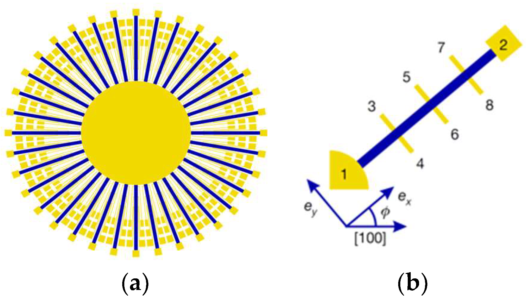
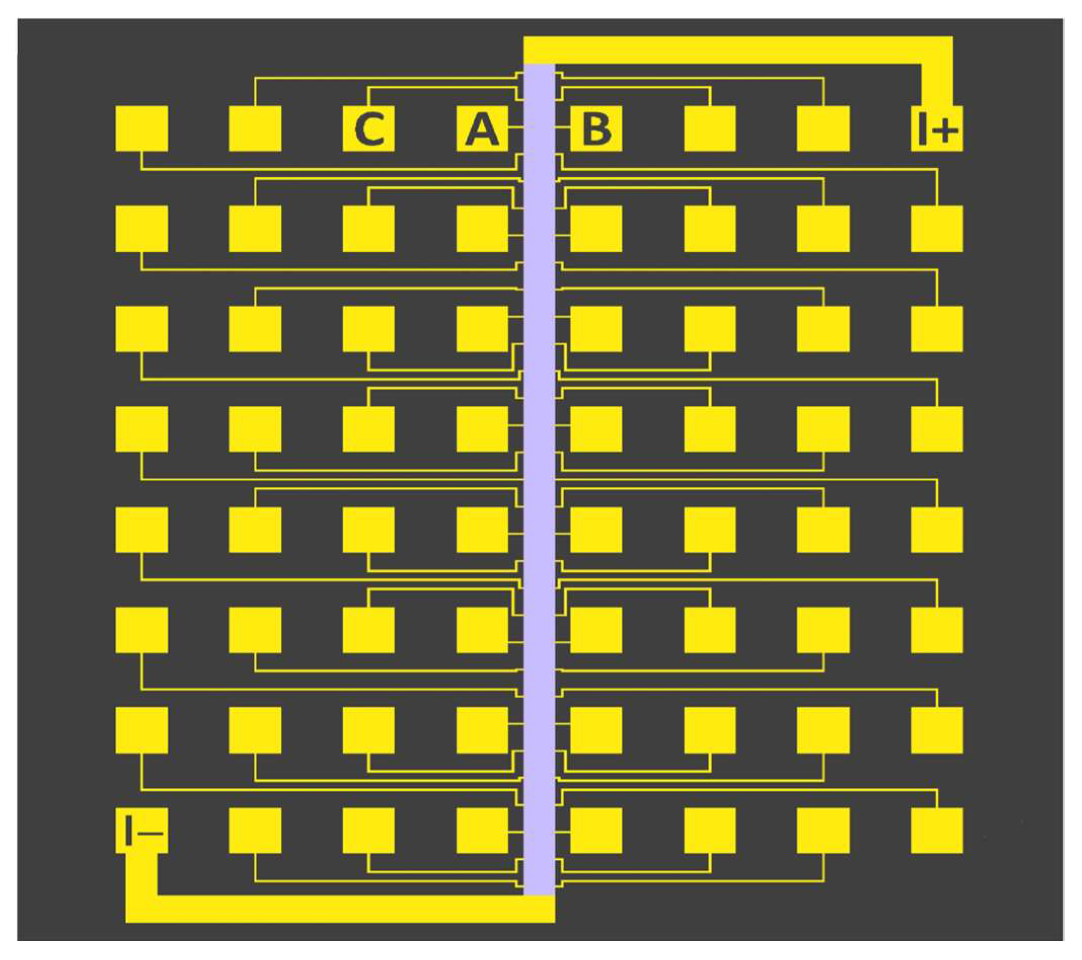
To determine whether the resistivity is isotropic or not, one should measure the angular dependence . For that purpose, we designed the “sunbeam” device pattern illustrated in Figure 1. The sunbeam consists of 36 Hall bars at an angle from one another. The LSAO substrates are cut and polished with the edges parallel to the crystallographic [100], [010], and [001] directions with an accuracy better than . We align the mask to the substrate edges under the microscope, and the resulting deviation of the lithographic direction from the crystallographic [001] orientation is less than . The electrical transport is measured in each Hall bar. In Figure 1b, the current flows from the contact 1 to 2 and the transverse voltage is measured along the y-axis, e.g., between 3 and 4. Our device has three pairs of transverse contacts, so we define VT ≡ (V34 + V56 + V78)/3. Other than this averaging, all the data are presented as measured. To factor out the current and the geometry, we introduce the transverse resistivity T ≡ (VT/I)d, where I ≡ I12 is the probe current and d is the film thickness. Using this 36-beam pattern, we can measure in 72 devices and in 108 devices, with the angular resolution of . We will refer to this as angle-resolved resistivity (ARR) and angle-resolved transverse resistivity (ARTR) measurements, respectively.
Why bother with ARTR when ARR is more direct and easier to understand? The answer is in the “error bars”, which are, here, the ubiquitous device-to-device variations. In the semiconductor industry, even after many decades of developments in synthesis and fabrication, the state-of-the-art on-chip device uniformity is a couple of percent; in the case of HTS cuprates, even that benchmark has been elusive. Then, if the anisotropy of resistivity, , is large, the sinusoidal dependence will stick out and above the noise. The problem is that the actual anisotropy in LSCO is generally very small, less than 1%, in most of the (x, T) phase diagram. This is the reason why it remained undetected for so long.
ARTR is more sensitive than ARR by one or two orders of magnitude because it is background-free; it probes off-diagonal components of the resistivity tensors, which in isotropic (C4-symmetric) samples must be zero by symmetry. Note that most of the techniques mentioned in Section 1.1 above (with the notable exceptions of the cross-polarized Raman spectroscopy, second-harmonic generation, and THz dichroism) also probe diagonal elements and are thus subject to large backgrounds.
A caveat: this cuts both ways. By the same token, ARTR is also very sensitive to the C4 symmetry being broken by any external factors. For this reason, a single measurement on a single sample is generally not sufficient; one needs a systematic examination of a large set of samples and parameters, and then the systematic trends in the dependences on T, B, and x can indeed differentiate unambiguously, as will be shown below.
1.5. Key Experimental Observations: Unexpected Transverse Voltage
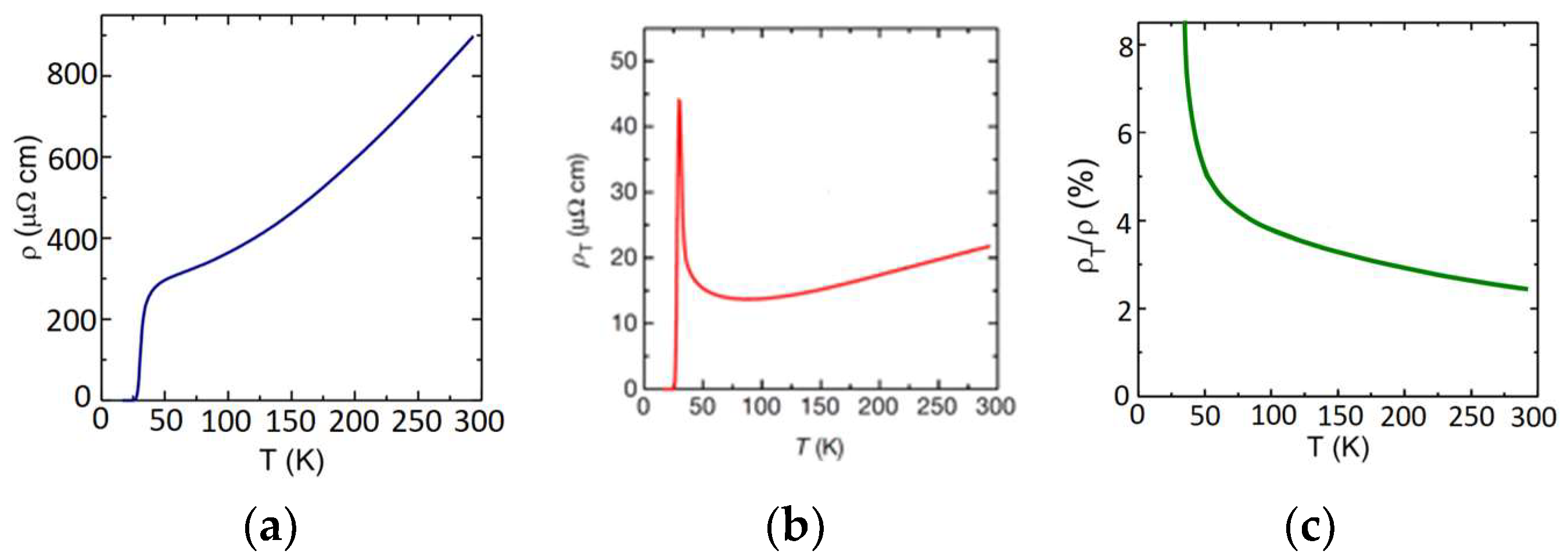
In Figure 2a, we show the temperature dependence of the longitudinal resistivity for one representative doping, p = 0.10. (This parameter p is not measured directly but is inferred from the measured Tc by assuming a putative parabolic relation, as we discussed in [29] and as it is customary; we use it to facilitate the comparison with the literature, but none of our conclusions depend on this convention.) The data agree with the previous results in the literature and show a superconducting transition at Tc ≈ 30 K. The same device, already at room temperature, shows a nonzero transverse voltage even without any magnetic field applied. This means that the corresponding transverse resistivity is nonzero, as shown in Figure 2b, and hence, the fourfold rotational symmetry (C4) is broken.
Temperature dependence of. Figure 2b shows that as T is lowered, decreases gradually and changes its slope for T < 70 K. A prominent and sharp peak in appears in the vicinity of the superconducting transition in the temperature range where various techniques observe superconducting fluctuations. The ratio , which is a measure of transport anisotropy, in fact decreases with temperature, as one would expect; nevertheless, at this doping level (p = 0.10), it remains finite and measurable even at room temperature.
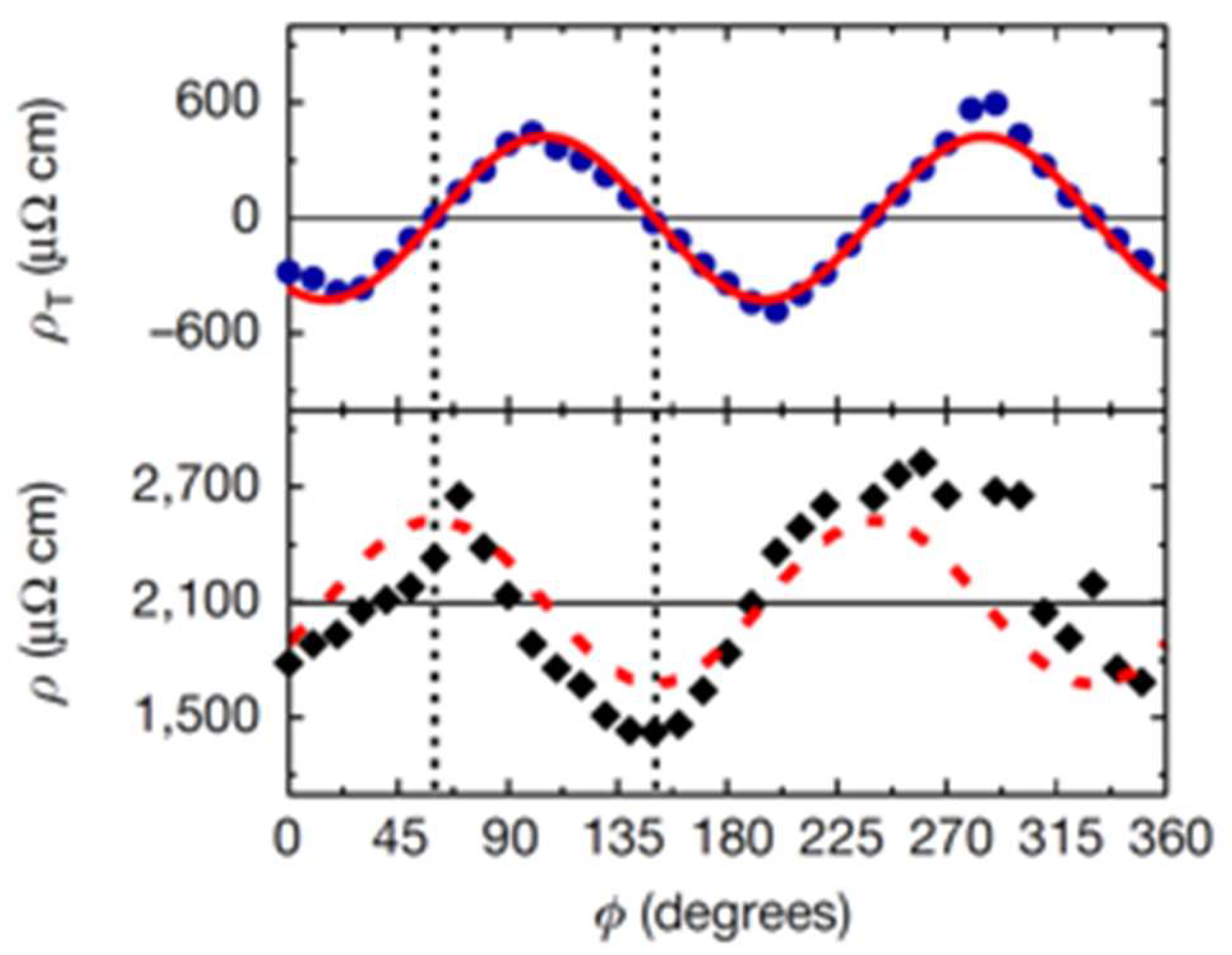
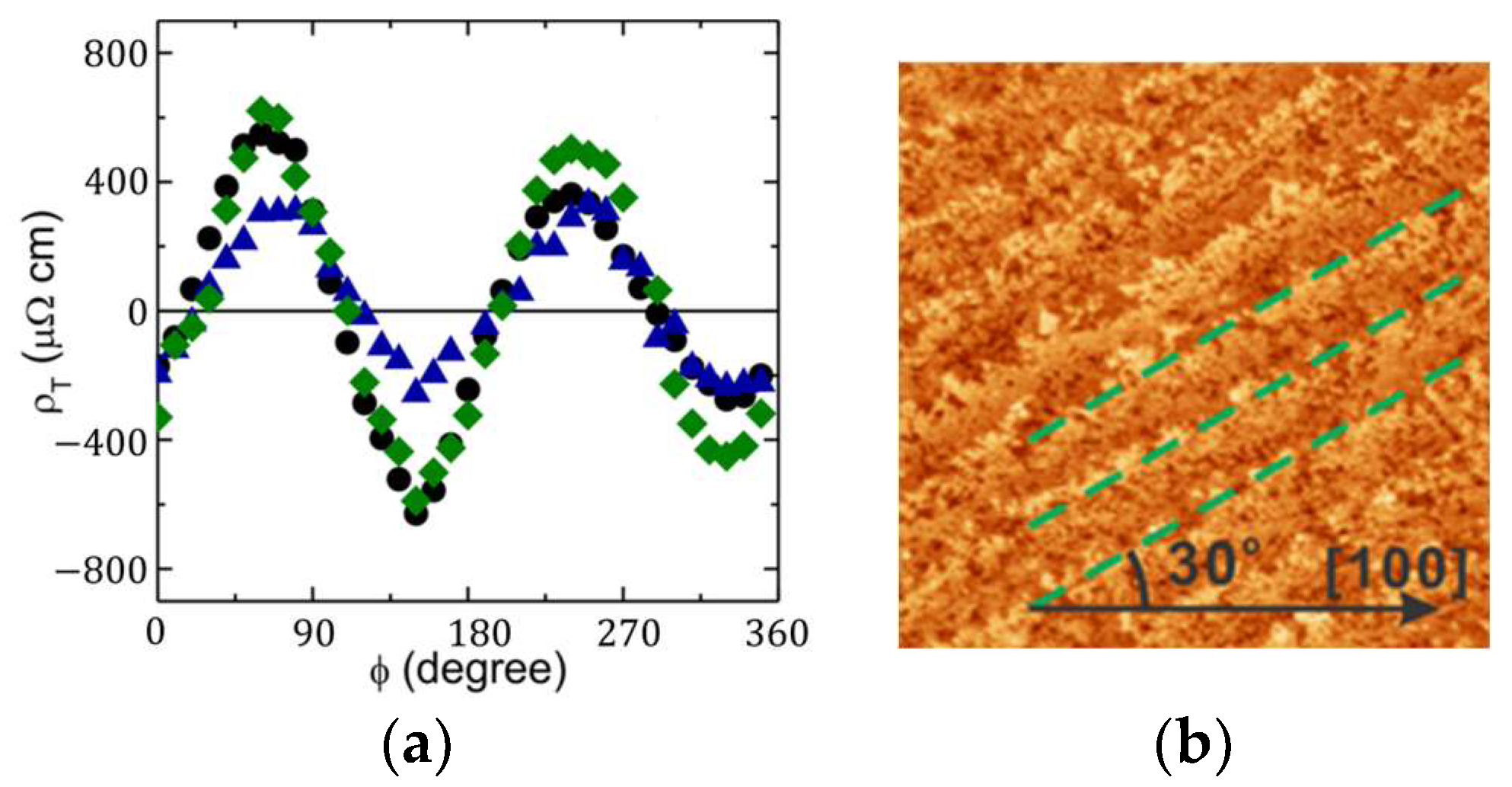
Angular dependence of. As an example, in Figure 3, we show and data measured at 36 angles in an LSCO (p = 0.04) film patterned into a sunbeam at T = 30 K. The raw experimental data (blue dots in the upper panel) fit very well to with and (the solid red curve). The lower panel shows the experimental data (solid black diamonds). The dashed red line is not an independent fit; it was generated by just translating the solid red line up by and to the left by . The agreement is reasonable but not nearly as good as for the data because of the on-chip device-to-device variations in the “background” longitudinal resistance. This clearly illustrates the advantages of the background-free ARTR technique.
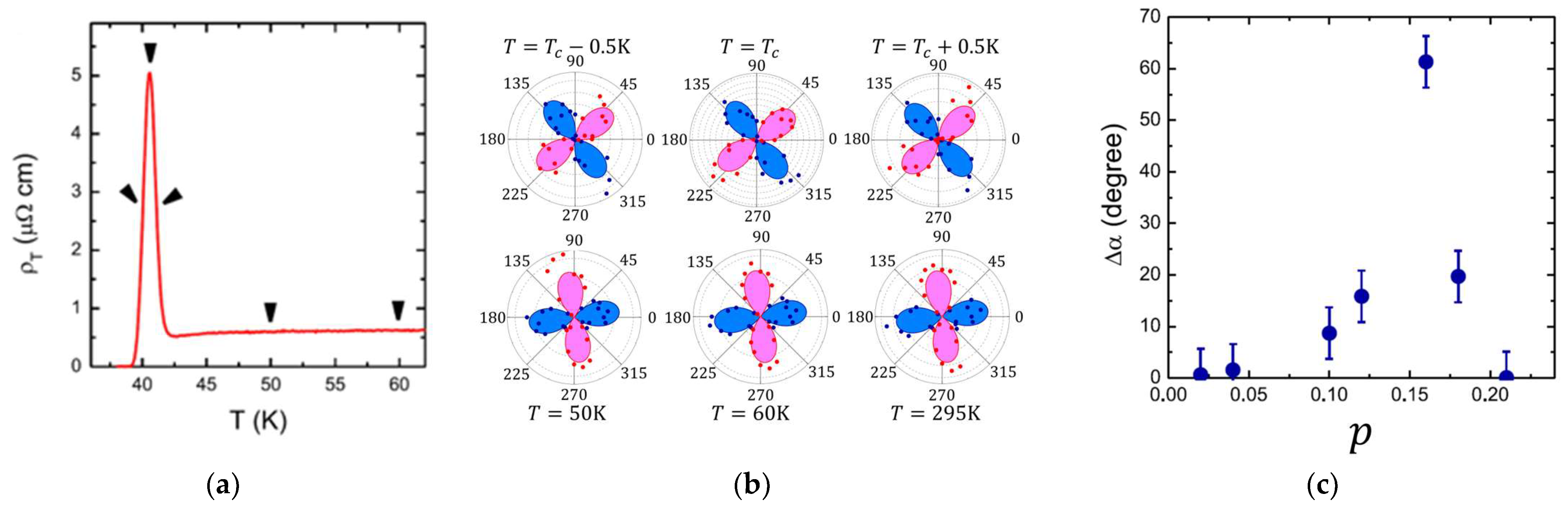
Rotation of the nematic director with the temperature. In Figure 4a, we show the data for an optimally doped (p = 0.16) LSCO film at one fixed azimuth angle. In Figure 4b, we show the fully angle-resolved data for the same sample at six fixed temperatures. In these polar plots, the radial distance measures the magnitude of as a function of the azimuth angle . The red color is used for positive and blue for negative values. Comparing the six panels, one can see that as the temperature is lowered, the principal axes of the resistivity tensor change their orientation with respect to the [100] crystal direction. The apparent rotation of the nematic director is strong in the relatively narrow temperature region near Tc.
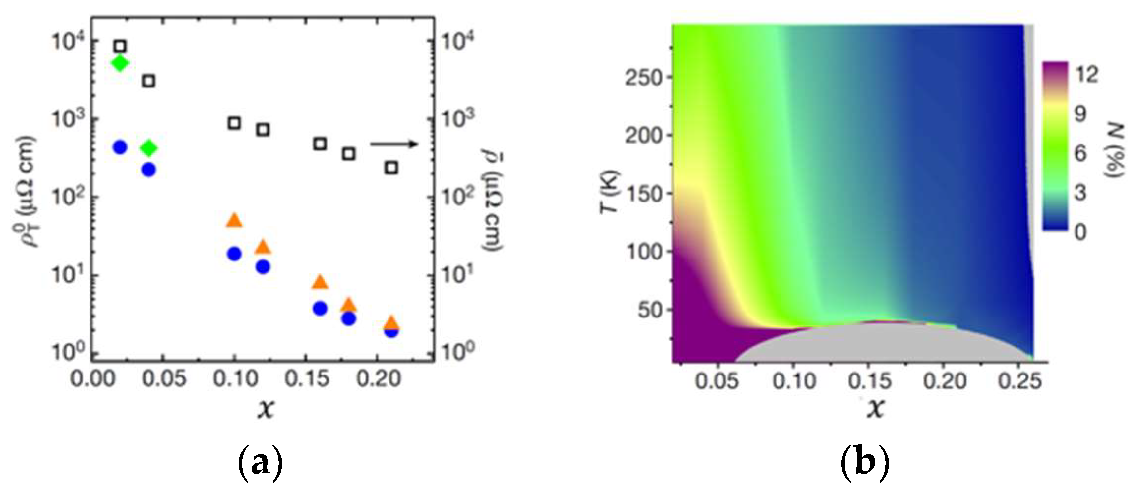
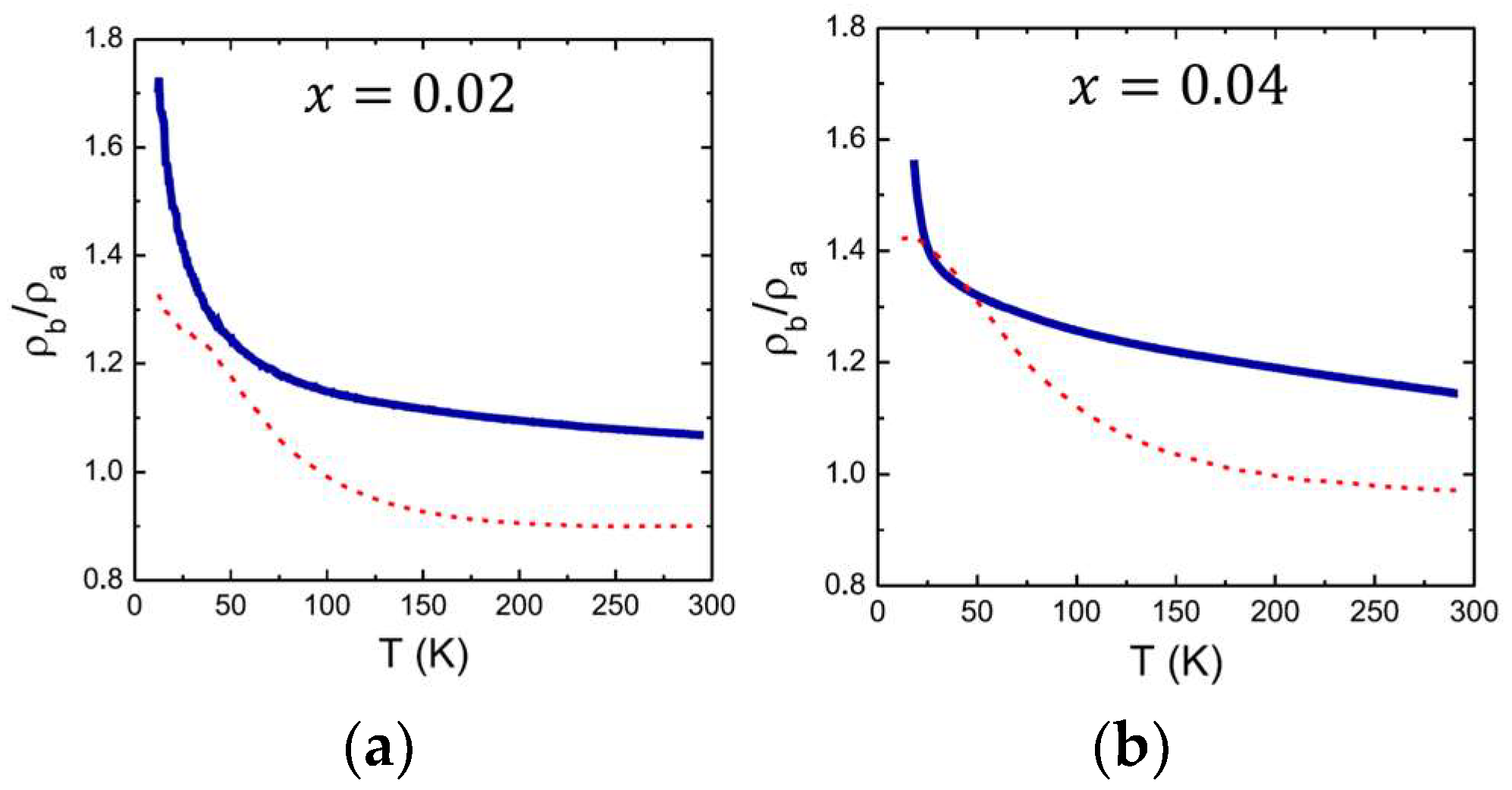
Doping dependence of. In LSCO, the ratio varies strongly and systematically as a function of the level of chemical doping x from more than 50% for x = 0.02% to less than 0.5% for x = 0.22 (see Figure 5).
Time and length scales. In Figure 1b, the width of one Hall-bar device is 100 µm, and the distance between two contacts for the longitudinal voltage measurements is 300 µm. The entire sunbeam circle diameter is 5 mm. The observed dependence for the 36 Hall bars of one sunbeam pattern implies that C4 symmetry is broken on the 5 mm scale. The time it takes us to complete one set of T-dependent ARTR measurements is typically on the scale of several days to weeks. Again, the observed dependence means that the anisotropy map is stable over at least that time scale. We remeasured a few sunbeam devices after storing them for extended periods (years), and these did not show any changes.
Temperature cycling. The sunbeam pattern (Figure 1a) has 253 gold contacts. The number of lead wires in our cryogenic transport measurement setups is limited to 48 to keep the thermal load reasonably low and to be able to reach down to T = 0.3 K. This means that we cannot measure all the Hall bars simultaneously. Rather, we wire-bond to subsets of contacts and make the T-dependent measurements on the corresponding devices. Then, we warm the system up, take the film out, and remove these wires. Then, we rewire another segment and perform another set of T-dependent measurements, etc., until the whole pattern is covered. Thus, to map one complete set of ) and curves, it takes several room-temperature-to-low-temperature (4 K or 0.3 K) cycles. Again, the observed dependence means that nematicity’s overall orientation and amplitude are robust against thermal cycling between room temperature and low temperature. A possibility remains that this could change if the film is heated to some higher temperature. Still, we consider it unlikely since it was shown that several samples with the same doping—all of which were synthesized at —have very similar nematicity amplitude and director orientation.
The organization of this paper. The above examples illustrate our typical experimental observations of nonzero transverse resistivity in LSCO films. Since the crystal structure of these films is essentially tetragonal, one is tempted to attribute this observation to a new and exciting physical phenomenon, electronic nematicity. However, before jumping to that conclusion, one should carefully consider, and rule out by firm experimental evidence, the possibility of any extrinsic factors, such as experimental artifacts or the film’s inhomogeneity, that might generate a nonzero transverse voltage. In this review, we ponder all such artifacts that we could think of and discuss in detail how we have ruled them out in our experiments. The aggregate evidence seems to disqualify this scenario overwhelmingly.
2. Reproducibility and Statistics
We observed spontaneous transverse voltage in LSCO films at BNL for the first time in 2006. Our first thought was that this is just an artifact due to a slight misalignment of the voltage contacts—a well-known (even if frequently brushed off) problem in Hall effect measurements. Before long, it became clear that this was not the cause—the effect we saw was too large, by two orders of magnitude, and independent of the lithography mask we used. Our following hypothesis was that this arises from sample inhomogeneity since it was known in the literature that this could cause anisotropic vortex flow. Again, soon it became clear that this was not the case, either. Subsequently, we thoroughly scrutinized and double-checked for a dozen other conceivable artifacts and extrinsic causes and ruled them out one by one in a series of experiments that involved thousands of LSCO films and devices and took over a decade to complete. After we exhausted all the alternatives, we convinced ourselves that the effect is almost undoubtedly intrinsic and (in 2017) published our first report [1]. Reassuringly, all the experimental data acquired since then, by us and others, also point to the same conclusion.
In more detail, two lithographic patterns were used in our studies of the spontaneous transverse voltage. The first contains a single strip, 10 mm long and oriented (to within accuracy) along the crystallographic [100] direction. It is provided with 32 pairs of symmetric contacts, as shown in Figure 6. This pattern offers 30 devices (‘pixels’) for the measurements of longitudinal resistivity and 31 devices for the measurements of transverse resistivity . Using custom-made high-throughput (parallel) measurement set-ups, we can study all of these devices simultaneously [3]. We measured at discrete temperatures (e.g., T = 40 K, 50 K, …, 300 K) in over 3000 such LSCO devices. In about 200 devices, we continuously measured from T = 300 K down to T = 4 K and, in a few dozen devices, down to T = 0.3 K.
The second pattern is the sunbeam structure (Figure 1a) that allows for measuring in 72 devices and in 108 devices [1]. We use it to study the dependence of and on the azimuth angle , with resolution. In LSCO films, we measured at T = 300 K in approximately 2000 such devices and the continuous T-dependence of in about 1000 devices.
The critical experimental fact is that we observed a spontaneous (i.e., zero-field) transverse voltage in all these LSCO films and devices, without exception. Nonzero is seen at all doping levels and up to room temperature. It is substantial and reproducible in repeated measurements on the same film or device and even on different films if the doping level is kept the same. Most importantly, shows systematic and smooth dependences on the device orientation, temperature, and doping. It is difficult to reconcile such systematics with the hypothesis that the effect originates from some random, extrinsic factors.
3. Artifacts
3.1. Contact Misalignment
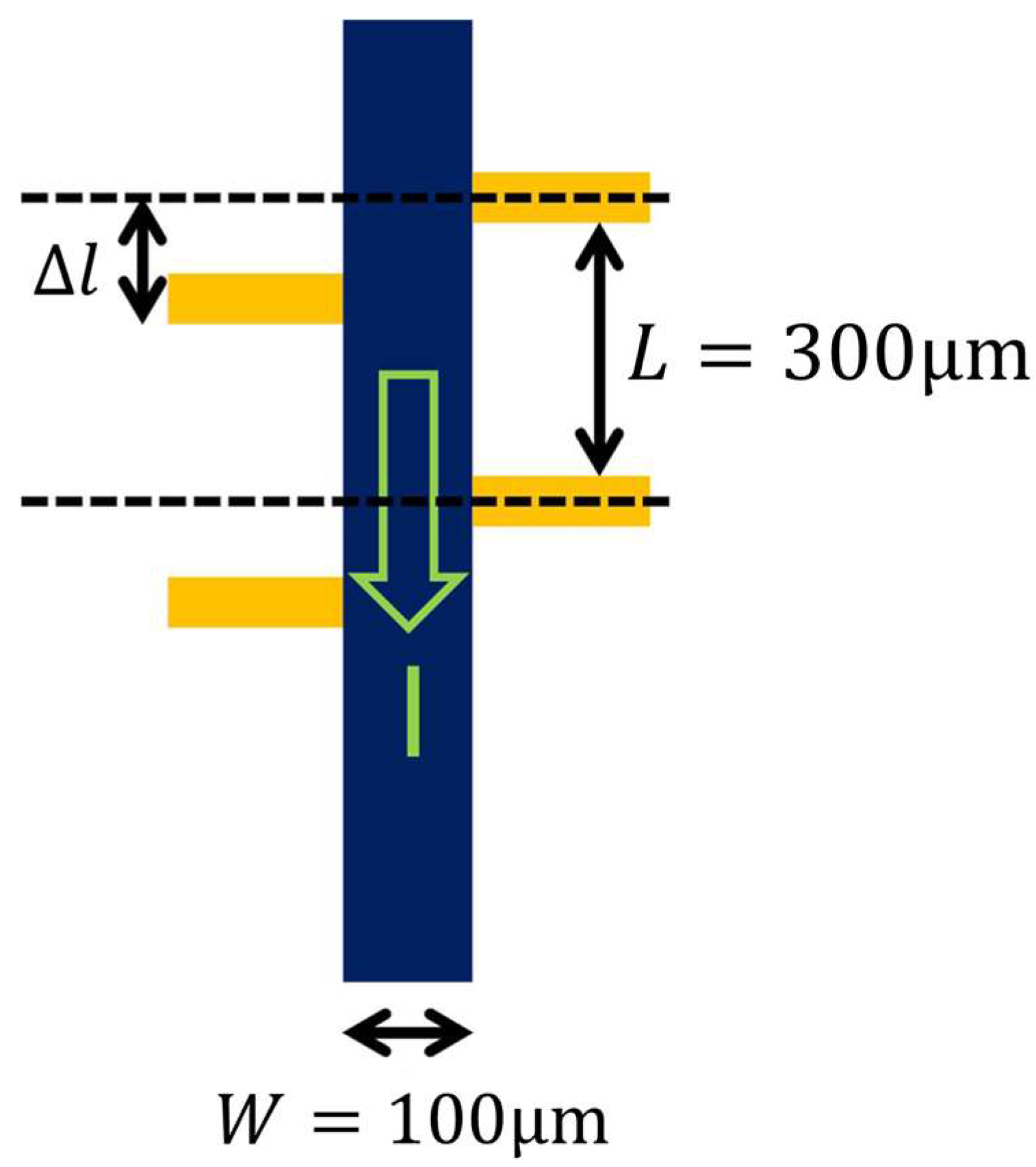
We use a pair of opposite voltage contacts to measure the transverse voltage, e.g., {3, 4} in Figure 1b. Ideally, these contact pads should be perfectly aligned, but in any experiment, some misalignment is inevitable, as schematically illustrated in Figure 7. This gives rise to the voltage , where is the contact displacement, L is the distance between the contacts used to measure the longitudinal resistance R, and I is the probe current. This voltage can be substantial if, for example, the electric connections are made by attaching the wires to a bulk crystal or a pellet sample using the silver paste, as is the standard practice. To alleviate this problem, we use a lithographic process to precisely pattern our films into devices for transport measurements. In this approach, the upper limit of the contact misalignment is determined by the precision in the fabrication of the lithography mask, which in our case is . This cannot account for the actual we observe for the following reasons.
- The observed effect is way too large. In the lithography pattern we used (Figure 1), the width of the Hall bar is W = 100 µm, and the distance between the two neighboring voltage contacts is L = 300 µm. Assuming, conservatively, the upper limit for the misalignment, l = 0.5 µm, this would give and . However, this is much smaller than the experimental value in Figure 2c, where at room temperature, while near Tc it surges to 30%. To produce such a big effect, the contact misalignment would have to be 30 µm, and that would be visible under an optical microscope or even to the naked eye.
- does not scale with. From the above formula, the ratio is determined solely by the value of , so it should be independent of the temperature. However, this contradicts our experimental observations; as illustrated in Figure 2, the ratio varies significantly with T, increasing very steeply near Tc.
- does not scale with. We demonstrated that both and vary strongly and systematically with the azimuth angle —they oscillate with the same amplitude and period () while they are phase-shifted by from one another, as shown in Figure 3. The misalignment of transverse voltage contacts certainly cannot explain the observed angular dependence of the longitudinal resistivity, .
- does not scale with. We studied the dependence of and in LSCO as a function of the level of chemical doping x and found that the ratio varies strongly and systematically with x, from more than 50% for x = 0.02 to less than 0.5% for x = 0.22 (see Figure 5). Since we used the same lithography mask to fabricate all these devices, the contact misalignment should not change with x.
Altogether, we conclude that although the alignment of the voltage contacts in our transport devices is not perfect, the contribution to the measured from the contact misalignment is negligible in our experiments.
3.2. Orthorhombic Distortion
In free-standing LSCO crystals, there is a structural phase transition to orthorhombic structure below some temperature Torth, which decreases with doping and vanishes at x ≈ 0.22. While this orthorhombic distortion breaks the D4h symmetry in principle, it cannot account for the observed nematicity in LSCO thin films.
- The observed effect is way too large. The orthorhombic distortions in our films are suppressed because the films are very thin (20-unit-cells thick) and epitaxially anchored to the tetragonal LaSrAlO4 (LSAO) substrates. In consequence, the crystal structure of our LSCO films is almost exactly tetragonal at all doping levels. To be quantitative, X-ray diffraction data in twice-thicker LSCO films grown on LSAO substrates by ALL-MBE show the in-plane orthorhombic distortion of just 0.08% in insulating, 0.04% in optimally doped, and 0.01% in overdoped metallic LSCO films, respectively [31]. Hence, even at the lowest doping levels, the orthorhombic distortion in films is quite small—at least a factor of 20 smaller than in the corresponding bulk samples—and the distortion energy must be reduced even more. Consider a charge-density wave (CDW) in the simple Peierls’ model for a rough estimate. The total CDW condensation energy E(Q) should scale as , where Q is the distortion amplitude. Using this rule of thumb, the estimated E(Q) in our thin films should be about three orders of magnitude smaller than in the bulk crystals, i.e., basically negligible.
- does not depend on substrate. As a control experiment, we deposited LSCO on orthorhombic NdGaO3 (NGO) substrates. In these substrates and the thin LSCO films grown on top, the orthorhombic distortion is substantial, with , where a and b are the in-plane lattice constants. Nevertheless, we found that the amplitude of nematicity, was nearly the same in these orthorhombic LSCO films as in the tetragonal LSCO films on LSAO substrates. The only difference was that in the films on NGO, the nematic director was pinned to the crystallographic [100] direction. In contrast, in the LSCO films on LSAO, the angle was generally different and dependent on doping and temperature.
- does not depend on uniaxial pressure. In the second control experiment, we used a custom-built mechanical clamping device to apply uniaxial pressure on LSCO films grown on LSAO substrates. We could achieve up to 0.9% uniaxial strain and orthorhombic distortion. However, we found no effect on the amplitude of nematicity [32], consistent with paragraph 2 above. Note that this distortion is larger than the one spontaneously occurring in free-standing LSCO crystals (0.8% in undoped La2CuO4 and decreasing with Sr doping).
- The temperature dependence ofdoes not match. In free-standing bulk LSCO crystals, orthorhombic distortion develops in a mean-field manner and becomes nearly constant below about 0.5 . In stark contrast, shows a strong peak near Tc, rising by a factor of 5–10 in a narrow temperature interval above Tc.
3.3. Strain
Since LSCO is orthorhombic in bulk but is constrained to be tetragonal by the epitaxy with LSAO, our LSCO films on LSAO are under anisotropic compressive strain. We were made aware of speculation that this could, in principle, give rise to nonzero VT. How this could actually work is unclear to us. Nevertheless, the same arguments as in Section 3.2 above also rule out this scenario.
3.4. Substrate Miscut
Nominally, the surfaces of the LSAO substrates we used in these experiments were polished perpendicular to the crystallographic [001] direction. However, in reality, there is always a slight misalignment in the to range. Because of this ‘miscut,’ atomic steps occur at the substrate surface. The miscut orientation varies randomly from one substrate to another, and the alignments of atomic steps differ accordingly. We use an atomic force microscope (AFM) to image the orientation and density of atomic steps in every LSAO substrate (before the film deposition) and LSCO film (after the growth). Because of our atomic-layer-by-layer growth, the steps in the LSAO substrate are projected into the LSCO film, giving rise to antiphase dislocations and domain boundaries. These break the rotation and mirror-plane symmetries in the film, so in principle could generate nonzero VT. However, we can rule out this scenario based on the following arguments.
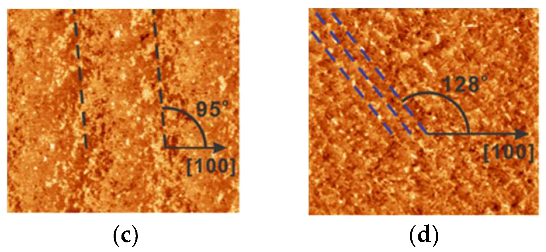
- does not depend on the miscut angle and orientation. We have investigated in detail whether there is a correlation between the step orientation and the uniaxial anisotropy in the electronic transport, i.e., the direction in which the maximum of occurs. Since the miscut angle varies randomly from one substrate to another, the same is true of the density and orientation of the surface steps. However, the nematicity amplitude and director orientation are reproducible in the films with the same doping level, while they vary systematically with doping and temperature. This is illustrated in Figure 8, where we present AFM images of three LSAO substrates, each showing clear atomic steps. The postgrowth AFM scans of the LSCO films deposited on these LSAO substrates confirmed that the steps were carried over into the films to the surface. The densities and orientations of atomic steps vary significantly from one to another of these three films (Figure 8b–d). Yet, both the amplitude and the phase of the angular oscillations of remain nearly the same (Figure 8a).
- is the same in films and bulk. We also observed nematicity in bulk single crystals of LSCO, with the amplitude essentially the same as in LSCO films doped to the same level. Our data agree with those obtained independently by other groups [6,7]. These millimeter-thick bulk LSCO crystals have neither misfit nor antiphase dislocations, and the atomic steps at the surface have an unmeasurably small effect on the transport properties. Altogether, the observed in both LSCO films and bulk crystals cannot originate from surface steps.
3.5. Thermal Gradient
If the temperature at the two transverse contacts is not the same, this can generate thermopower, i.e., a nonzero transverse voltage. This, however, cannot account for the observed nematicity.
To minimize the thermal gradient, we used the Helium-4 and Helium-3 cryogenic systems in which the sample is surrounded by exchange gas. We reach temperatures down to T = 4.2 K and T = 0.3 K, respectively, with temperature stability better than ±1 mK [35]. The thermopower is exceedingly small because the temperature variation across our 1 cm × 1 cm sample is less than 1 mK.
To avoid device self-heating, in our transport measurements, we keep the excitation current density low, at 80 A/cm2. This corresponds to the probe current Ix = 2 µA, while I-V relations are linear up to at least 10 µA for both V and VT contacts.
Thermopower should be even under the current reversal, while VT that we measure is odd.
One would not expect the angular dependence of thermopower to be d-wave-like.
It is difficult to see why thermopower would show an exponentially strong dependence on the doping level x.
3.6. Thickness Gradient
It is not uncommon that, because of the geometry of the deposition system, the film thickness is not perfectly uniform, and the film may be thinner on one side than on the other, particularly if one is using a single-target pulsed-laser deposition or sputtering. The beam flux from such a source decreases with the distance from the beam center; hence, the local deposition rate varies with the position on the substrate. In this case, even if the film resistivity is perfectly isotropic, the measured resistances parallel () and transverse () to the thickness gradient direction may differ. However, we can rule out this scenario given the following arguments.
- Our ALL-MBE system is equipped with a scanning quartz-crystal oscillator monitor, which enables the measurement of the local deposition rates across the substrate [9]. If we use a single thermal effusion cell, the deposition rate varies linearly across the substrate, and the gradient is 4% per 1 cm. However, we compensate for this gradient by using a pair of identical sources placed symmetrically (at azimuth angles that differ by 180°). The resulting gradient is thus much less than 1% over 1 cm, so the variations across a single 100 µm wide Hall bar are negligible.
- We digitally control the film thickness by monitoring the intensity of the Reflection High-Energy Electron Diffraction (RHEED). By scanning the RHEED beam across the film surface, we can verify that the thickness is uniform. Moreover, we can also see that the RHEED pattern and the atomic termination of the film surface are the same across the entire wafer.
- The geometry of the synthesis system determines the variations in film thickness. These should reproduce from one film to another, while we see that has a strong and systematic doping dependence.
- Moreover, strongly depends on temperature, and so does the orientation of the nematic director. That rules out any purely geometric origin.
- Within this scenario, the measured would always be proportional to the measured , at every temperature, the azimuth angle , doping, etc., which is at variance with the experimental facts.
3.7. Composition Gradient
Similar arguments also rule out the hypothesis that the observed nonzero transverse voltages could originate from a gradient in the film composition.
- Since the geometry of our MBE system fixes our source positions and orientations with respect to the substrate, such gradients would not change from one film to another if the targeted film composition is kept the same.
- This would change with the doping level, but the doping dependence would be the opposite of what we see. The effect (if any) of such a gradient would increase with doping (it would scale with x). We see that decreases fast with doping, by a few orders of magnitude, until, on the extremely overdoped side, we hit the noise floor (see Figure 5). To throw in some numbers, if, for example, the residual gradient was 1% over 1 cm, for x = 0.20, this would amount to , while for , it would be 10 times smaller, i.e., . In contrast, the observed nematicity amplitude is, in fact, more than an order of magnitude larger in LSCO, with rather than .
- The nematicity amplitude varies strongly and systematically with the temperature, while the gradient in doping level would not depend on T.
- Moreover, had this been the culprit, the observed nematic director would always point in the same direction, while its orientation, in fact, changes substantially with the doping level and temperature.
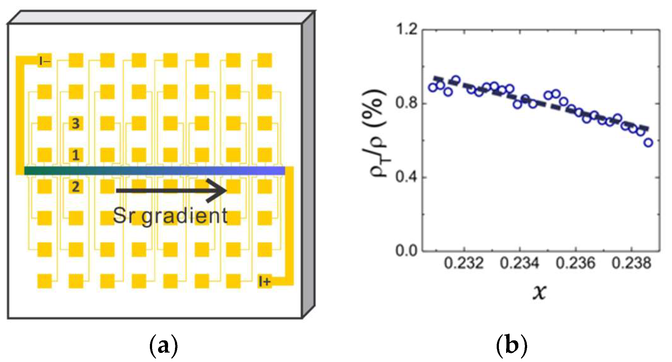
To double-check this, we synthesized an overdoped LSCO film with the deliberate gradient in the Sr doping level, 4% over 1 cm length. This is the largest gradient we can generate in our present MBE system by using just a single Sr source, aimed at the angle of with respect to the substrate surface. We described the details of this combinatorial-MBE (COMBE) technique before [1,30,36], but for self-contentedness, let us summarize the salient points here. “Doping x” in Figure 10b refers to the Sr content in La2-xSrxCuO4 (LSCO). We measure x using quartz-crystal microbalance (QCM), Rutherford back-scattering, X-ray reflectance fringes, etc., to the aggregate absolute accuracy of a few percent. On the other hand, using our COMBE technique, we can generate a 4%/cm linear gradient of x in one direction. This is just a geometrical effect, so it can be calculated very accurately. We verified this by direct measurements using our scanning QCM as well [30]. We pattern the strip into 32 pixels; then, the difference in x between two neighboring pixels is Dx = 0.04/32 x = 0.00125 x. Near optimal doping, this gives Dx = 0.0002. So, while we do not know the absolute value of x to better than a few percent, we know the relative pixel-to-pixel change with two-orders-of-magnitude-better precision. Thus, we can look at the doping dependence in exquisitely fine steps. This is very valuable if, e.g., one is studying scaling and critical exponents near a doping-controlled quantum phase transition [36].
The point here is that we indeed observe nematicity in each pixel in this linear combinatorial library. The ratio decreases linearly with doping (see Figure 10). This is the opposite of what one would expect if the observed nematicity originated from the Sr doping level gradient.
3.8. Schottky Barrier Contacts
The possibility that could just be the voltage offset due to some contact imperfections can also be ruled out. Our gold contact pads are thick and large, and the contact resistances are very low. Moreover, we always check the dependence of both the longitudinal and the transverse voltage on the probe current. We verify that the and characteristics are linear and Ohmic, up to well above the probe current used in our and measurements, at all temperatures above .
4. Sample Inhomogeneity
A nonzero transverse voltage could arise even if the contacts are perfectly aligned but the sample is not homogeneous and the current flow is distorted. This could happen for many reasons: because of some structural defects such as scratches in the substrate and/or the film; because the films are multiphase, polycrystalline, granular, and disordered; or because the stoichiometry is not uniform, including, e.g., distribution of dopants, interstitial oxygen, or oxygen vacancies. Such imperfections occur in every sample, even if they remain undetected. In principle, any of these could cause the direction of the current near the transverse voltage contacts to deviate from the Hall-bar orientation; then, these two voltage contacts need not be at the same equipotential. Nevertheless, based on detailed and quantitative arguments listed in the following, we can rule out any of these as the principal cause of the transverse voltages we measure in LSCO.
4.1. Phase Separation
Complex oxides have complex phase diagrams with many phases. Some of these phases can be thermodynamically more stable than the targeted one; hence, once nucleated, they will proliferate at the expense of the desired phase. For these reasons, most high- cuprate samples contain inclusions, precipitates, or grains of unwanted phases. In addition, cuprates are prone to various intrinsic instabilities and competing ordering tendencies, including antiferromagnetism, charge-density waves (CDW), spin-density waves (SDW), etc. These competing phases can form islands and domains, which can be elongated and oriented and/or have an anisotropic distribution, thus making the sample conductivity nonuniform and/or anisotropic on a macroscopic scale. However, we do not believe this can account for the observed nematicity for the following reasons.
- Our LSCO films are not granular. The X-ray diffraction and atomic force microscopy (AFM) studies indicate that the crystalline structure and morphology of our LSCO films are very uniform both microscopically and macroscopically. According to RHEED, high-resolution XRD, AFM, scanning cross-section transmission electron microscopy (STEM), etc., our LSCO films synthesized by ALL-MBE are single crystals, atomically smooth, and nearly perfect. This results from 30 years of sustained and focused development of the ALL-MBE technique and technology [36,37,38,39,40,41]. No static ordered phase (CDW, SDW, ferro- and antiferromagnetism) is observed in the entire doping range, while some nematicity is always present. While CDW and AF fluctuations may be present, these would average to zero with time and space and would not be macroscopically aligned.
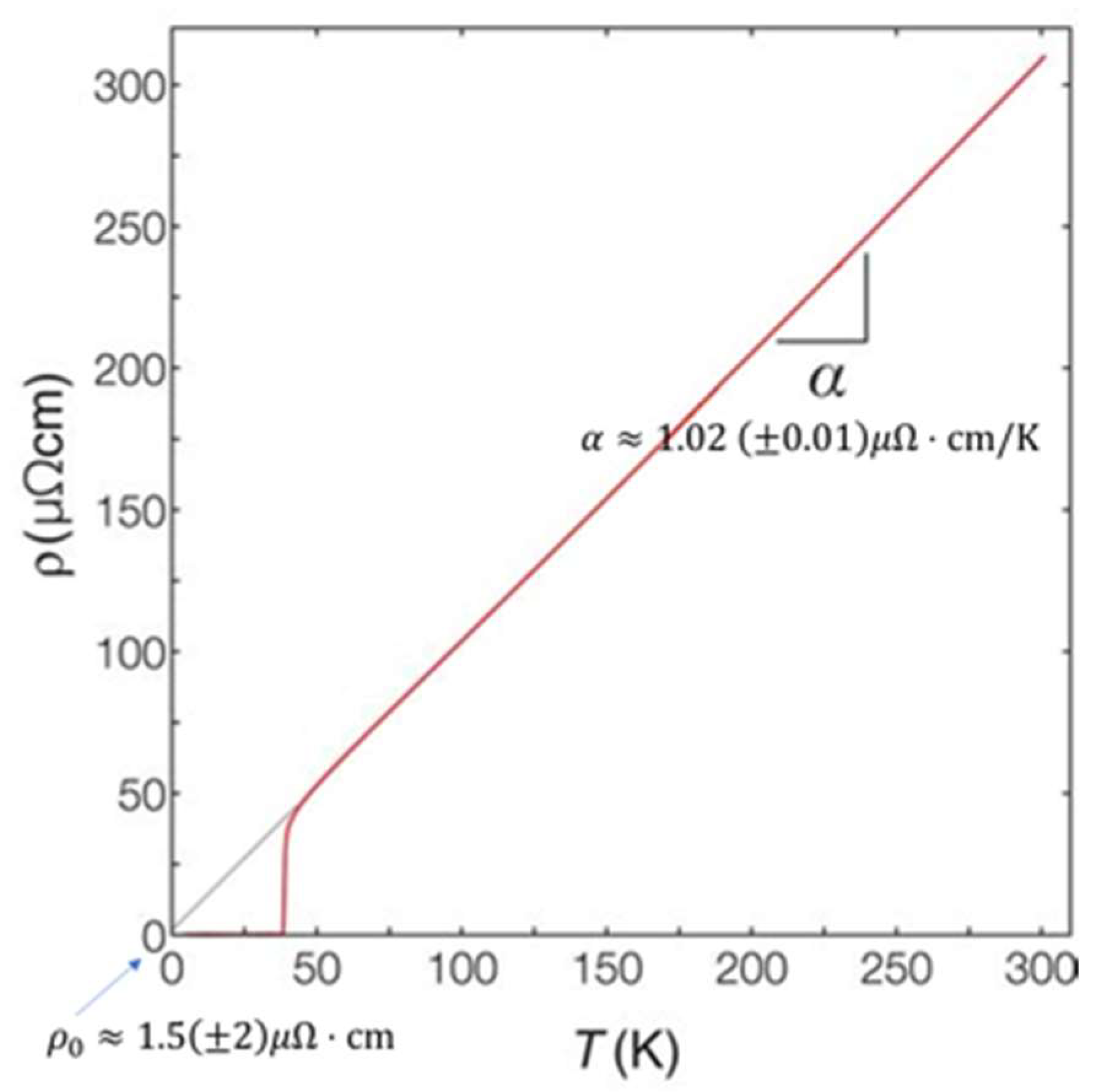
- Our LSCO films are ‘clean’. One figure of merit, frequently used in the literature to benchmark the film quality, is the residual resistivity or, more tellingly, the residual resistivity ratio (RRR), defined as . In Figure 11, we show the dependence in a representative LSCO film that we synthesized using ALL-MBE, while the measurements were carried by an independent group (at NHMFL) [41]. It shows that , and RRR > 200. By this standard, this (single-crystal) LSCO film is more perfect and less disordered, by far, than any bulk LSCO single-crystal reported in the literature. Suppose one uses the standard Drude formula and inserts the measured and broadly accepted values for the Fermi velocity, effective mass, and carrier density; the inferred mean free path would be longer than 1.7 µm, i.e., more than 4000 lattice constants. This should be considered exceptionally clean within the accepted standards and terminology [42]. An alternative is to postulate a breakdown of the canonical description of metals and superconductors. Nevertheless, this film shows a substantial nonzero transverse resistivity already at room temperature and down to Tc. It also features a pronounced peak near , while no such peak exists in the longitudinal resistivity. Moreover, changes the sign four times as the in-plane angle varies [1]. Therefore, is proportional neither to nor to the derivative
- is linear in T. In a clean unconventional superconductor with a V-shaped d-wave gap, the dependence of the superfluid density on temperature is expected to be linear. Scattering on any disorder, impurities, and other defects would cause the breaking of near-nodal pairs, filling in the gap and rounding it near the node, and leading to the dependence of below some characteristic temperature T*. We have shown that in LSCO, is linear for all doping levels, in some films down to 1 K. This is only expected in a very clean d-wave superconductor [29].
- anddependences are systematic. The strong, smooth, and reproducible dependences of the nematicity amplitude and orientation on and , impose very tight constraints on any model. It is difficult to account for all of these within any inhomogeneity scenario. Handwaving is not sufficient—one ought to present a concrete model of inhomogeneity that can at least qualitatively reproduce the dependence of coincident with the dependence of at fixed T and doping; the decrease in with x; the rotation of the nematic director with T, B, and x; the disappearance of the peak in with B [43], etc.
4.2. Guided Vortex Motion
Several studies reported the observation of transverse voltage in cuprates near Tc and attributed this to a peculiar motion of superconducting vortices [44,45,46]. In cuprates, thermally generated superconducting vortices and antivortices abound at temperatures near Tc as low-energy excitations. Suppose that, for whatever reason, the current direction deviates locally from the Hall-bar direction. In that case, the vortex motion will have a component along the current path, generating a voltage between the transverse contacts [44,45,46]. The same could happen even if the electric current is strictly parallel to the Hall-bar direction if the vortex motion is constrained and guided, e.g., by spatially organized pinning or barriers. However, given the following experimental evidence, we can rule out this scenario.
- In one device, and for one pair of voltage contacts, a scratch, a microcrack, or local inhomogeneity in oxygen distribution could redirect the current locally, thus generating a transverse voltage. It is almost impossible to believe, though, that this could, just by chance, happen at all 108 positions measured and in such a way to create a curve in every film and for every doping.
- Even if the guided vortex motion was relevant for explaining the pronounced peak in near Tc, such as in Figure 2b, it could not be at the origin of the electronic nematicity we observe at room temperature, where no superconducting vortices are present.
- The hypothesis of guided vortices is also incompatible with our angle-resolved transverse magnetoresistance (ARTMR) data [43]. If the moving vortices are preferentially driven in a particular direction—by a gradient in the distribution of dopant ions or some other defects, step edges and antiphase dislocations due to substrate miscut, etc.—one could expect some anisotropic transverse voltage because of broken C4 symmetry, and this could peak near Tc. However, as more vortices are generated, this effect should grow stronger with the magnetic field. Moreover, one would also expect to see the same effect in the longitudinal resistivity. This is the opposite of what we observe. First, the peak near Tc in decreases by an order of magnitude in the field B = 6 T. Second, there is no peak (and almost no MR whatsoever) in at the same temperature and field. Third, if the sample were effectively orthorhombic due to some compositional or structural reasons, one would expect this to change neither with the magnetic field nor with the temperature, while the nematicity magnitude and director orientation show a strong and systematic T- and B-dependence [43].
4.3. Randomness of Sr Doping
Several groups have suggested that some of the unusual observations in overdoped LSCO, including the demise of Tc and the superfluid density with doping, may be attributed to a peculiar distribution of the Sr dopant atoms. This scenario may warrant a separate section because of a semantic ambiguity—should this be called extrinsic or intrinsic. As far as it is known, Sr dopants distribute randomly; LSCO is a solid solution. Hence, this randomness is unavoidable for entropy reasons and, in this sense, is intrinsic to the thermodynamically stable form of LSCO. Strictly speaking, this disorder breaks down all spatial symmetries, both translational and rotational. However, XRD in LSCO shows sharp Bragg peaks [31]. Moreover, at least in overdoped LSCO, angle-resolved photoemission spectroscopy (ARPES) shows sharp quasiparticles and a well-defined Fermi surface, also confirmed by the study of angle-resolved magnetoresistance oscillations (AMRO). Hence, LSCO behaves quite like a crystal and is generally modeled assuming long-range order and crystallographic-space-group symmetry, which should manifest itself in all macroscopic physical properties. However, our ARTR experiments show that the rotational symmetry is broken in electrical transport, while the detailed findings do not seem consistent with any Sr-distribution-related scenario.
- This randomness averages out on the relevant (µm, mm) length scales. The average Sr–Sr distance is smaller than 1 nm, and since the distribution of Sr atoms is random, local variations are expected on a very small (nm) scale. However, this randomness should be averaged out already on the scale of, say, 100 nm. It should be thoroughly washed out on the scale of the width of a single Hall bar, 100 µm, and even more so on the scale of the sunbeam device illustrated in Figure 1a, which is larger than 0.5 cm.
- Sr clustering is not seen by structural probes. In one proposed model, the density of Sr atoms is assumed to vary locally, forming domains or clusters. However, this hypothesis can be refuted based on the arguments listed in Section 4.1, which rule out phase separation and granularity of whatever origin. Sr clusters have been observed neither by nanoscale synchrotron-based techniques such as X-ray fluorescence nor by TEM-based high-resolution electron-energy-loss spectroscopy (HR-EELS).
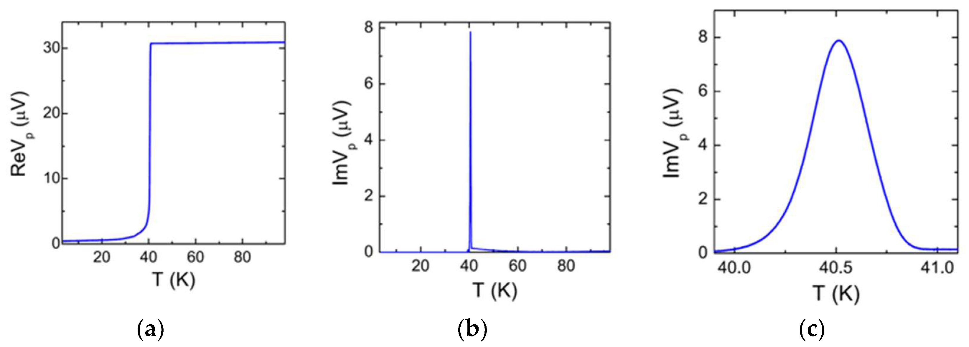
- Sr clustering is inconsistent with the transport and susceptibility data. In Figure 12, we show the two-coil mutual inductance data for an optimally doped (x = 0.16) LSCO film. The in-phase signal measures the reactive response and shows the Meissner effect with a sharp onset at Tc = 40.8 K. The half-width-at-half-maximum of the peak in the out-of-phase (dissipative) response puts an upper limit on the variations of Tc in this film, , over a large area of 10 × 10 mm2. Using the empirically known relations that link , and x, one can estimate the corresponding upper limit on the gross local variations in . For , and assuming the worst-case scenario when the variation is in the form of a gradient along one line, this would result in measured —at least two orders of magnitude smaller than the anisotropy we measure near Tc. This rules out attribution to a substantial inhomogeneity in the film of the observed phenomena, including, in particular, the peak in VT near Tc, which is typically 1–2 orders of magnitude broader.
- Sr clustering is inconsistent with thedependence. The probability that sufficiently large domains, with a large enough difference in stoichiometry, could be present in our films is quite small. However, let us grossly overestimate it as P = 10% for one device. What, then, is the probability that this happens in each of the 108 devices we fabricate out of one film, and that this happens in such a way as to generate the dependence on the azimuth angle, with the shift between and , as shown in Figure 3. Essentially, it is null. Moreover, inhomogeneity would have to be organized on a macroscopic scale in such a way that (a) the film shows a preferred transport direction, (b) when the film is ‘sliced’ into 108 small devices, this remains the same in each device, in both magnitude and orientation, (c) this reproduces in other films of the same doping, and (d) as we change the doping level, this “organized inhomogeneity” would need to have a smooth and monotonic doping dependence. More is different here; our extensive statistics allow for definitive statements and rule out the dominant role of such random agents.
- Sr clustering is inconsistent with thedependence. The systematic temperature dependence, particularly the director rotation, is the ultimate challenge to the Sr-clustering model and any other scenario based on random or organized chemical or structural disorder. The Sr distribution does not change with the temperature.
4.4. Tc Distribution
Segal et al. [47] considered a model of an inhomogeneous superconductor in which Tc shows some spatial variations. They found that this model can account for a sizeable transverse resistivity within the temperature interval , where Tc1 is the lowest and Tc2 the highest value. In this case, scales with the temperature derivative of the longitudinal resistivity . This proportionality, , is the fingerprint of the distribution of Tc in the sample.
In our films, the resistive transition shows some broadening, say . Then, at first glance, this appears to be a plausible explanation, at least for the peak in near Tc. However, a more detailed analysis clearly shows that this cannot be the key contributing factor for several reasons.
- Not at room temperature. This mechanism only works near Tc, where R(T) drops sharply. It does not work at room T, where R(T) evolves gradually. Even if the observed broadening of the resistive transition originated entirely from the disorder and inhomogeneity—which, as we argue in detail in (vi) below, is decidedly not the case—it is unclear how this could account for the observed nematicity at room temperature.
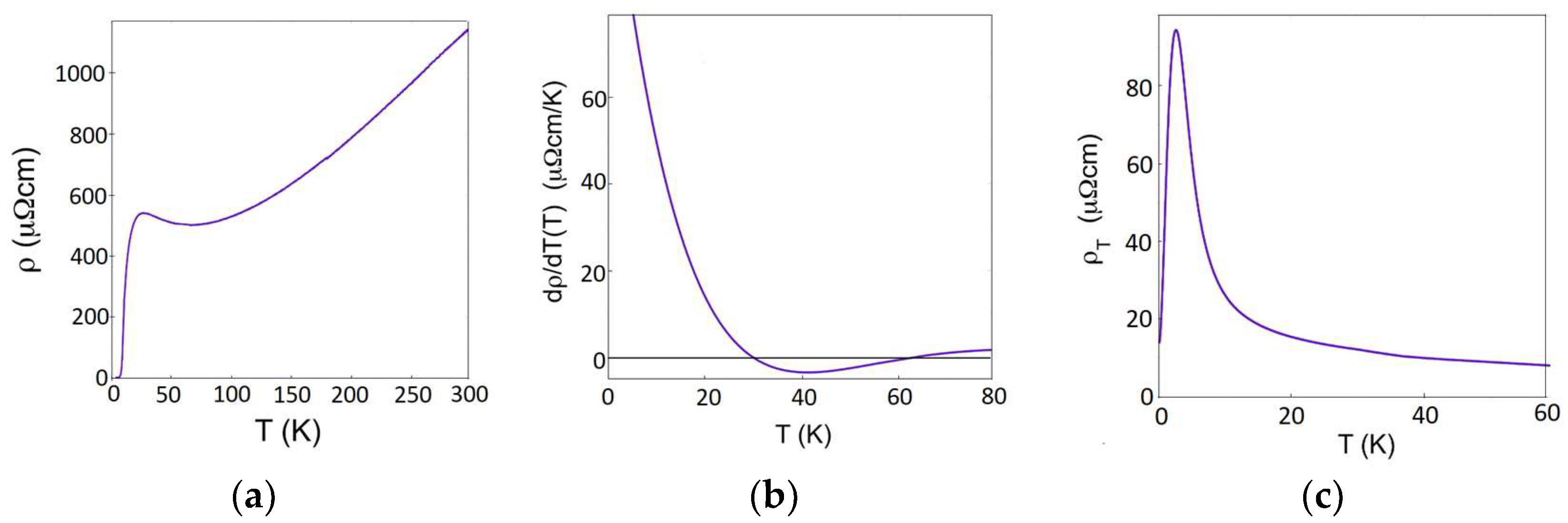
- Not for x ≲ 0.07. As shown in Figure 13, in LSCO with x = 0.063, the dependence is not monotonous. As T decreases, decreases (like in metal) but then flattens and starts to increase (like in a semiconductor) until it starts dropping fast again in the region near Tc where superconducting fluctuations take over. Hence, the derivative changes sign twice with temperature. In contrast, always stays positive. For , LSCO is neither superconducting nor metallic; is semiconductor-like, and is negative in the entire range . In contrast, is always positive in this temperature interval.
- Not for. As we mentioned in Section 1.5 (ii) above, , and, hence, for . On the other hand, , so for , , while for , . Since neither nor is zero anywhere above Tc, clearly, .
- Not random; systematic x-dependence. Here, inhomogeneity means the randomness of some structural and electronic features at different locations in the film. If this was the dominant source of VT and if we systematically measure at various locations along a strip that is patterned in the film, the recorded should either vary randomly with the position, if the domains are relatively large, or be constant (i.e., independent on the position) if the domains are much smaller than the strip width, and thus, averaged out. To test this possibility, we synthesized an LSCO film with a built-in continuous gradient in doping level x by means of the combinatorial molecular beam epitaxy (COMBE) [30,36]. Then, we used lithography to pattern this film, as shown in Figure 10a. This pattern, with 2 current contacts and 31 pairs of voltage contacts, allows us to measure and at 30 positions in the LSCO film with a continuous doping gradient. We built the corresponding electronics that allow us to measure all 30 channels simultaneously, thus reducing the scatter due to possible variations in temperature, etc. As seen in Figure 10b, the measured ratio shows a linear dependence on p; clearly, it is not random at different locations in the film.
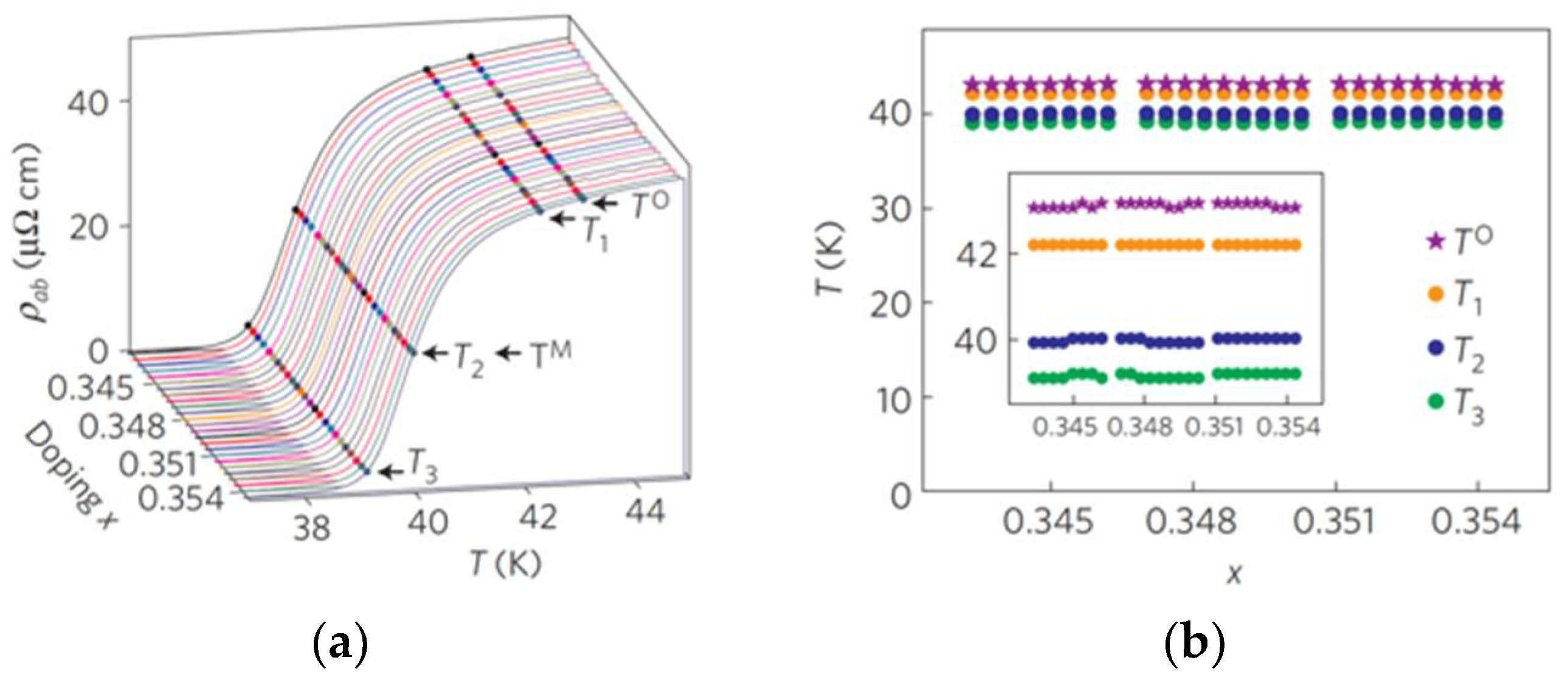
- Broadening of the resistive transition in cuprates does not arise from disorder. In Section 4.3 (iv) above, we showed that in our LSCO films, the spread in Tc, as measured by the mutual inductance technique, can be as small as ±0.1 K over the 10 × 10 mm2 area. On the other hand, in LSCO (and all other superconducting cuprates), the resistive transitions are quite broad [42], typically, DTc ≈ 5–10 K. The actual value is somewhat vague since various definitions of Tc are possible and indeed have been used in the literature, e.g., the transition onset TO; the temperature at which the resistivity drops to 90%, 50%, or 10% of the normal-state value just above the onset, etc. However, all of these suffer from ambiguity in the choice of the normal-state resistivity. It is less subjective to use the temperature TM at which the slope of is the largest; this can be determined unambiguously as the temperature at which the derivative curve, , reaches the maximum. The most conservative choice, however, and the one we always adhere to, is to use the temperature at which the sample resistivity vanishes, i.e., Tc ≡ T(R = 0). We found (with extensive statistics) that this is also the temperature at which the Meissner effect onsets. Using this definition, we find that Tc (as determined by high-precision mutual inductance measurements) is quite sharp. In Figure 14, we show a set of characteristics measured in one LSCO film patterned into a linear combinatorial library of devices [30]. For each device, we indicated the transition onset TO, the temperature T1 at which the resistivity drops to 90%, T2 where it drops to 50%, T3 at which it drops to 10%, and TM at which the derivative has the maximum. It is apparent from Figure 14b that, as long as we consistently use any of these characteristic temperatures, it stays essentially constant, on the scale of 0.1 K, in all devices across the entire film.
- Broadening of the transition in cuprates arises from superconducting phase fluctuations. The resolution of this apparent ‘paradox’—the simultaneous occurrence of a very sharp Meissner signal and a broad resistive transition—is well-known [42,48,49,50,51,52].
- Cuprates are extreme type-II superconductors with the ratio , where is the London penetration depth and the coherence length. Therefore, one indeed expects, from the Ginzburg–Levanyuk criterion, that there should be a few Kelvin-wide temperature regions in which superconducting fluctuations dominate the transport. As the temperature is increased, vortex–antivortex pairs are generated and thermally dissociated. The probe current causes free vortices to move, and vortex flow causes dissipation and finite resistance [42].
- In LSCO, at every doping level, the superfluid density is very low, i.e., a few orders of magnitude lower than in conventional superconductors such as Nb or Pb. Expressed in the units of Kelvin, the phase stiffness is nearly equal to Tc [29]. This fact implies that thermal phase fluctuations essentially determine the superconducting transition by destroying the global phase coherence [52].
- Cuprates are quasi-two-dimensional—they behave like vertical stacks of intrinsic Josephson junctions. A single LSCO layer can host HTS with Tc, with the superfluid density equal to that in the bulk samples [29]. Hence, in cuprates, one should expect to see Berezinskii–Kosterlitz–Thouless (BKT)-like physics. Indeed, dynamic BKT transition has been observed by MHz susceptibility measurements [48] and microwave [49] and THz spectroscopies [50,51].
- Almost every type of experiment that could detect thermal phase fluctuations in principle has shown that in cuprates, they persist in a vast temperature region. Both ARPES and scanning tunneling microscopy (STM) data show that the superconducting gap does not close at Tc but persists well above, up to as much as 1.5 Tc. Microwave and THz spectroscopies show superconducting phase fluctuations up to 20–30 K above Tc [49,50,51]. Magnetoresistance data show superconducting fluctuations well above the critical field that causes nonzero resistance. In underdoped LSCO, evidence for superconducting vortices at temperatures as high as 250 K has been found in the Nernst effect, diamagnetism, torque magnetometry, etc.
5. Control Experiments Using Ti Films
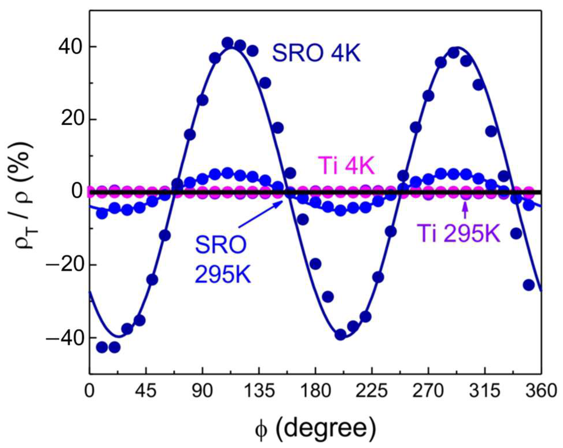
As one more control experiment, we performed a complete ARTR study of a thin film of titanium, a well-studied conventional metal in which there are no reasons to expect electronic nematicity. The Ti film was deposited at room temperature, so it is polycrystalline and isotropic in plane, and one expects to be zero at every angle by symmetry. If we observe nonzero oscillating as , this must originate from some artifacts due to lithography and/or measurement techniques. Checking this is a rigorous test of our ARTR methodology.
We deposited a 16 nm thick Ti film on (001) Si substrate by e-beam evaporation and patterned it using photolithography into a sunbeam device as described in Figure 1a. We used the same lithography mask and procedure to pattern this Ti film, the LSCO films [1,2], and the Sr2RuO4 (SRO) films [26]. ARTR measurements were made using the same experimental setup. To compare all these films on the same footing, we normalized the measured by the corresponding average longitudinal resistivity . In Figure 15, we compare the ARTR data for Ti and SRO. Apparently, in sharp contrast to large and oscillating in SRO and LSCO, is zero within the noise in the Ti film.
6. Nematicity beyond ARTR in LSCO
6.1. Other Cuprates
Essentially everything that we discussed in Section 1, Section 2, Section 3, Section 4 and Section 5 above pertains equally to other cuprates, while it introduces some new, material-specific problems. YBa2Cu3O7-d is orthorhombic, and it contains layers of Cu-O chains that run preferably in one direction. This causes anisotropy in electron transport that originates from the crystal structure; this must be carefully discerned and subtracted before asserting the presence of additional electronic nematicity. Moreover, the chain layers are typically disordered, which also needs to be considered.
Bi2Sr2CaCu2O8 (BSCCO) is also orthorhombic for a different reason: the BiO layers are buckled along the diagonal, forming a superstructure modulation with a period of about five lattice constants. While the in-plane lattice constants are not very different, ; a significant transport anisotropy again originates from the crystal structure. Substituting Pb at Bi sites has been shown to reduce the amplitude of this superstructure modulation. Hence, studying BSCCO with and without Pb substitution may be a way to discern between the anisotropy that originates from the lattice and the purely electronic contribution.
Hg- and Tl-based cuprates may be better in these aspects, but unfortunately, they are not amenable to ALL-MBE synthesis, or for that matter, any in situ film-growth methods. The reason is that they contain volatile atomic species (Hg and Tl) which cannot be contained in films grown at temperatures high enough to form the ordered crystal structure (typically 600–700° and even higher). To achieve the desired stoichiometry, such films are typically postannealed ex situ in the appropriate (Hg- or Tl-rich) atmosphere, but the resulting films tend to be granular, have rough surfaces, etc.
6.2. Bulk Crystals
A few caveats discussed in Section 3 are specific to thin films and not relevant for bulk-crystal LSCO samples. For example, films are generally strained by epitaxy to a lattice-mismatched substrate, while the free-standing crystals are strain-free. However, all the other concerns—e.g., the problems with contacts, misalignment, sample geometry, etc.—remain and, in principle, must be addressed. Some are even aggravated. In most cuprates, oxygen is volatile and mobile. When a crystal is formed out of the melt by cooling, under a constant oxygen pressure, the oxidation power increases, and oxygen is driven in [53]. However, the oxygen insertion process is diffusive and may be self-limiting if the preferential diffusion paths involve oxygen vacancies. As the temperature is lowered, the time needed to reach the homogeneous equilibrium distribution of oxygen diverges. Thus, the resulting oxygen distribution is inevitably inhomogeneous, with a higher oxygen concentration near the sample surfaces. A clear way to alleviate this problem is to equilibrate long enough at some high-enough temperature, then quench to the room or lower temperature as fast as possible, thus freezing a uniform distribution. However, to the best of our knowledge, this has not been conducted.
Bulk crystals are sometimes sculpted into Hall-bar devices using focused-ion beam (FIB) milling to reduce the geometric uncertainties and control the current direction. However, this introduces its experimental problems, notably the sample damage due to bombardment by high-kinetic-energy ionic species that get embedded or scatter sideways and disorder the sample. The same happens when, e.g., Pt or Au contacts are fabricated in situ using FIB-assisted deposition. Moreover, the FIB process is usually monitored in real-time by a scanning electron microscope (SEM). The beam of high-energy electrons also causes sample damage—and this need not be isotropic.
6.3. Other Techniques
As mentioned in the Introduction, many other techniques have been used to detect electronic nematicity. A detailed description of all of these is way out of the scope of the present review, so we will make just a few general remarks.
- Some techniques, such as scanning tunneling microscopy (STM) and angle-resolved photoemission spectroscopy (ARPES), are very surface-sensitive. Then, one needs to worry whether all the structural and electronic properties of the surface layer (that is probed) are the same as the bulk (that is not probed by ARPES or STM but is probed by transport or magnetic measurements to determine Tc). In fact, in most ionic crystals, it is guaranteed that the topmost surface layer will not have the bulk structure because of the long-range (Madelung) origin of the cohesion [31,54]. Here, BSCCO may be an exception because of the weak Van der Waals coupling between the layers (which also makes it cleavable).
- Most of these other techniques have background-related problems since one is looking for small angle-dependent deviations from some relatively large average value. Then, it is the question of how big these deviations are compared to the error bars and sensitivity of the measurement for one orientation.
However, a few of the techniques mentioned measure the off-diagonal elements, and are thus background-free, by symmetry. In this category are the measurements of THz dichroism, second-harmonic generation, and electronic Raman scattering in crossed-polarization geometry. These should, in principle, be more sensitive to weak signals of electronic nematicity.
7. Conclusions
Angle-resolved measurements of the transverse resistivity, ARTR, is a powerful method to detect anisotropy in electron transport. It measures the off-diagonal components of the electrical resistivity tensor, which in isotropic materials are zero by symmetry, so it is background-free and, hence, one to two orders of magnitude more sensitive than the standard measurements of the longitudinal resistivity. Combined with high-resolution structural studies such as those done by X-ray, electron, or neutron diffraction, ARTR can be used to unambiguously detect electronic nematicity, i.e., the breaking of the rotation symmetry of the crystal structure in the electron fluid.
However, ARTR is vulnerable to potential experimental artifacts and extrinsic factors like any other experimental technique. The latter include imperfect or misaligned electrical contacts, a crystal miscut, thermal gradients, variations in the film thickness or composition, and guided motion of superconducting vortices. A nonzero transverse voltage may emerge for each and any of these extrinsic causes. Hence, the proper usage of ARTR requires careful experimentation, meticulous materials science, and extensive statistics.
To establish the occurrence of electronic nematicity in LSCO, we performed an extensive study spanning over a decade and over 2000 samples. We addressed the possible artifacts in targeted experiments and eventually ruled out each possibility. We also showed that the hypotheses about phase separation, clustering of the Sr dopants, and other conceivable forms of sample inhomogeneity cannot consistently explain the massive data set that we have gathered or the well-established systematic trends and dependences of on the azimuth, temperature, magnetic field, and doping level.
Thus, we infer that the zero-field transverse voltage, which shows specific angular oscillations, is an effect intrinsic to the normal state of LSCO. It points to the spontaneous breaking of the C4 rotational symmetry in the electron fluid, i.e., the electric nematicity in copper oxide superconductors. At least for now, this appears to be the most plausible scenario. We feel that the burden of the proof is now with the nay-sayers. Handwaving is not sufficient—one ought to present a concrete model of something extrinsic that reproduces the dependence of and the dependence of at fixed T and doping, the decrease in with x, the rotation of the nematic director with T, B, and x, the disappearance of the peak in with B, etc. These are very tight constraints on any model.
As for the microscopic origin of the nematicity in LSCO, we remain agnostic. ARTR, per se, cannot answer this question. For this, ARTR must be combined with other techniques, including high-resolution structural and electronic probes, both static and dynamic, and the results must be compared to quantitative microscopic theories. We could make one comment with some confidence, though. Cuprates also feature another anomalous feature in their ‘normal’ state: a pseudogap in the single-particle density of states [55,56,57,58,59,60,61,62]. A natural question is how is this related to the nematicity we observed; could these two be just different manifestations of the same phenomenon? Comparing our nematicity data with the pseudogap studies in the literature, this seems unlikely. Pseudogap temperature T* decreases with doping, and above the critical doping p* = 0.19, the pseudogap was reported to disappear [60]. In contrast, we observe nematicity up to room temperature for p > 0.25. So, the relation between the two seems nontrivial.
Author Contributions
All the authors contributed to this review article. All authors have read and agreed to the published version of the manuscript.
Funding
The work at Brookhaven National Laboratory was funded by the DOE, Basic Energy Sciences, Materials Sciences and Engineering Division. X.H. was supported by the Gordon and Betty Moore Foundation’s EPiQS Initiative through grant GBMF9074.
Acknowledgments
This review draws extensively on previous research in collaboration with J. Wu, I. Robinson, H.P. Nair, J.P. Ruf, N.J. Schreiber, K.M. Shen, D.G. Schlom, J. Wardh, and M. Granath. Enlightening discussions on this topic with J. Zaanen, S.A. Kivelson, L.H. Greene, J.C. Davis, A. Chubukov, R. Fernandez, and E. Carlson are also gratefully acknowledged. We thank the reviewers for bringing several additional references to our attention.
Conflicts of Interest
The authors declare no conflict of interest.
References
- Wu, J.; Bollinger, A.T.; He, X.; Božović, I. Spontaneous breaking of rotational symmetry in copper oxide superconductors. Nature 2017, 547, 432–435. [Google Scholar] [CrossRef] [PubMed]
- Wu, J.; Bollinger, A.T.; He, X.; Božović, I. Detecting Electronic Nematicity by the Angle-Resolved Transverse Resistivity Measurements. J. Supercond. Nov. Magn. 2019, 32, 1623–1628. [Google Scholar] [CrossRef]
- Zaanen, J.; Gunnarsson, O. Charged magnetic domain lines and the magnetism of high-Tc oxides. Phys. Rev. B 1989, 40, 7391–7394. [Google Scholar] [CrossRef] [PubMed] [Green Version]
- Chandra, P.; Coleman, P.; Larkin, A.I. Ising transition in frustrated Heisenberg models. Phys. Rev. Lett. 1990, 64, 88–91. [Google Scholar] [CrossRef]
- Zaanen, J.; Oleś, A.M. Striped phase in the cuprates as a semiclassical phenomenon. Ann. Phys. 1996, 508, 224–246. [Google Scholar] [CrossRef]
- Kivelson, S.A.; Fradkin, E.; Emery, V.J. Electronic liquid-crystal phases of a doped Mott insulator. Nature 1998, 393, 550–553. [Google Scholar] [CrossRef] [Green Version]
- Oganesyan, V.; Kivelson, S.A.; Fradkin, E. Quantum theory of a nematic Fermi fluid. Phys. Rev. B 2001, 64, 195109. [Google Scholar] [CrossRef] [Green Version]
- Fradkin, E.; Kivelson, S.A.; Lawler, M.J.; Eisenstein, J.P.; Mackenzie, A.P. Nematic Fermi Fluids in Condensed Matter Physics. Ann. Rev. Cond. Mat. Phys. 2010, 1, 153–178. [Google Scholar] [CrossRef] [Green Version]
- Carlson, E.W.; Dahmen, K.A. Using disorder to detect locally ordered electron nematics via hysteresis. Nat. Commun. 2001, 2, 379. [Google Scholar] [CrossRef] [Green Version]
- Phillabaum, B.; Carlson, E.W.; Dahmen, K.A. Spatial complexity due to bulk electronic nematicity in a superconducting underdoped cuprate. Nat. Commun. 2011, 3, 915. [Google Scholar] [CrossRef]
- Fernandes, R.M.; Chubukov, A.V.; Schmalian, J. What drives nematic order in iron-based superconductors? Nat. Phys. 2014, 10, 97–104. [Google Scholar] [CrossRef] [Green Version]
- Beekman, A.J.; Nissinen, J.; Wu, K.; Liu, K.; Slager, R.-J.; Nussinov, Z.; Cvetkovic, V.; Zaanen, J. Dual gauge field theory of quantum liquid crystals in two dimensions. Phys. Rep. 2017, 683, 1–110. [Google Scholar] [CrossRef] [Green Version]
- Hinkov, V.; Haug, D.; Fauqué, B.; Bourges, P.; Sidis, Y.; Ivanov, A.; Bernhard, C.; Lin, C.T.; Keimer, B. Electronic Liquid Crystal State in the High-Temperature Superconductor YBa2Cu3O6.45. Science 2008, 319, 597–600. [Google Scholar] [CrossRef] [Green Version]
- Lawler, M.J.; Fujita, K.; Lee, J.; Schmidt, A.R.; Kohsaka, Y.; Kim, C.K.; Eisaki, H.; Uchida, S.; Davis, J.C.; Sethna, J.P.; et al. Intra-unit-cell electronic nematicity of the high-Tc copper-oxide pseudogap states. Nature 2010, 466, 347–351. [Google Scholar] [CrossRef] [PubMed] [Green Version]
- Daou, R.; Chang, J.; LeBoeuf, D.; Cyr-Choinière, O.; Laliberté, F.; Doiron-Leyraud, N.; Ramshaw, B.J.; Liang, R.; Bonn, D.A.; Hardy, W.N.; et al. Broken rotational symmetry in the pseudogap phase of a high-Tc superconductor. Nature 2010, 463, 519–522. [Google Scholar] [CrossRef] [Green Version]
- Mesaros, A.; Fujita, K.; Eisaki, H.; Uchida, S.; Davis, J.C.; Sachdev, S.; Zaanen, J.; Lawler, M.J.; Kim, E.-A. Topological Defects Coupling Smectic Modulations to Intra–Unit-Cell Nematicity in Cuprates. Science 2011, 333, 426–430. [Google Scholar] [CrossRef] [Green Version]
- Li, L.; Alidoust, N.; Tranquada, J.M.; Gu, G.D.; Ong, N.P. Unusual Nernst Effect Suggesting Time-Reversal Violation in the Striped Cuprate Superconductor La2-xBaxCuO4. Phys. Rev. Lett. 2011, 107, 277001. [Google Scholar] [CrossRef] [Green Version]
- Fujita, K.; Kim, C.K.; Lee, I.; Lee, J.; Hamidian, M.H.; Firmo, I.A.; Mukhopadhyay, S.; Eisaki, H.; Uchida, S.; Lawler, M.J.; et al. Simultaneous Transitions in Cuprate Momentum-Space Topology and Electronic Symmetry Breaking. Science 2014, 344, 612–616. [Google Scholar] [CrossRef] [Green Version]
- Lubashevsky, Y.; Pan, L.; Kirzhner, T.; Koren, G.; Armitage, N.P. Optical Birefringence and Dichroism of Cuprate Superconductors in the THz Regime. Phys. Rev. Lett. 2014, 112, 147001. [Google Scholar] [CrossRef] [Green Version]
- Cyr-Choinière, O.; Grissonnanche, G.; Badoux, S.; Day, J.; Bonn, D.A.; Hardy, W.N.; Liang, R.; Doiron-Leyraud, N.; Taillefer, L. Two types of nematicity in the phase diagram of the cuprate superconductor YBa2Cu3Oy. Phys. Rev. B 2015, 92, 224502. [Google Scholar] [CrossRef]
- Zhang, J.; Levenson-Falk, E.M.; Ramshaw, B.J.; Bonn, D.A.; Liang, R.; Hardy, W.N.; Hartnoll, S.A.; Kapitulnik, A. Anomalous thermal diffusivity in underdoped YBa2Cu3O6+x. Proc. Natl. Acad. Sci. USA 2017, 114, 5378–5383. [Google Scholar] [CrossRef] [PubMed] [Green Version]
- Chu, J.-H.; Analytis, J.G.; De Greve, K.; McMahon, P.L.; Islam, Z.; Yamamoto, Y.; Fisher, I.R. In-Plane Resistivity Anisotropy in an Underdoped Iron Arsenide Superconductor. Science 2010, 329, 824–826. [Google Scholar] [CrossRef] [PubMed] [Green Version]
- Chu, J.-H.; Kuo, H.-H.; Analytis, J.G.; Fisher, I.R. Divergent Nematic Susceptibility in an Iron Arsenide Superconductor. Science 2012, 337, 710–712. [Google Scholar] [CrossRef] [PubMed] [Green Version]
- Worasaran, T.; Ikeda, M.S.; Palmstrom, J.C.; Straquadine, J.A.W.; Kivelson, S.A.; Fisher, I.R. Nematic quantum criticality in an Fe-based superconductor revealed by strain-tuning. Science 2021, 372, 973–977. [Google Scholar] [CrossRef]
- Kuo, H.-H.; Chu, J.-H.; Palmstrom, J.C.; Kivelson, S.A.; Fisher, I.R. Ubiquitous signatures of nematic quantum criticality in optimally doped Fe-based superconductors. Science 2016, 352, 958–962. [Google Scholar] [CrossRef] [Green Version]
- Wu, J.; Nair, H.P.; Bollinger, A.T.; He, X.; Robinson, I.; Schreiber, N.J.; Shen, K.M.; Schlom, D.G.; Božović, I. Electronic nematicity in Sr2RuO4. Proc. Natl. Acad. Sci. USA 2020, 117, 10654–10659. [Google Scholar] [CrossRef]
- Cao, Y.; Rodan-Legrain, D.; Park, J.M.; Yuan, N.F.Q.; Watanabe, K.; Taniguchi, T.; Fernandes, R.M.; Fu, L.; Jarillo-Herrero, P. Nematicity and competing orders in superconducting magic-angle graphene. Science 2021, 371, 264–271. [Google Scholar] [CrossRef]
- Rubio-Verdú, C.; Turkel, S.; Song, Y.; Klebl, L.; Samajdar, R.; Scheurer, M.S.; Venderbos, J.W.F.; Watanabe, K.; Taniguchi, T.; Ochoa, H.; et al. Moiré nematic phase in twisted double bilayer graphene. Nat. Phys. 2022, 18, 196–202. [Google Scholar] [CrossRef]
- Božović, I.; He, X.; Wu, J.; Bollinger, A.T. Dependence of the critical temperature in overdoped copper oxides on superfluid density. Nature 2016, 536, 309–311. [Google Scholar] [CrossRef]
- Wu, J.; Pelleg, O.; Logvenov, G.; Bollinger, A.T.; Sun, Y.-J.; Boebinger, G.S.; Vanević, M.; Radović, Z.; Božović, I. Anomalous independence of interface superconductivity from carrier density. Nat. Mater. 2013, 12, 877–881. [Google Scholar] [CrossRef]
- Butko, V.Y.; Logvenov, G.; Božović, N.; Radović, Z.; Božović, I. Madelung Strain in Cuprate Superconductors—A Route to Enhancement of the Critical Temperature. Adv. Mater. 2009, 21, 3644–3648. [Google Scholar] [CrossRef]
- Bollinger, A.T.; Wu, Z.-B.; Wu, L.; He, X.; Drozdov, I.; Wu, J.; Robinson, I.; Božović, I. Strain and Electronic Nematicity in La2-xSrxCuO4. J. Supercond. Nov. Magn. 2020, 33, 93–98. [Google Scholar] [CrossRef]
- Ando, Y.; Segawa, K.; Komiya, S.; Lavrov, A.N. Electrical Resistivity Anisotropy from Self-Organized One-Dimensionality in High-Temperature Superconductors. Phys. Rev. Lett. 2002, 88, 137005. [Google Scholar] [CrossRef] [PubMed] [Green Version]
- Ando, Y.; Lavrov, A.N.; Komiya, S. Anisotropic Magnetoresistance in Lightly Doped La2-xSrxCuO4: Impact of Antiphase Domain Boundaries on the Electron Transport. Phys. Rev. Lett. 2003, 90, 247003. [Google Scholar] [CrossRef] [PubMed] [Green Version]
- Dubuis, G.; He, X.; Božović, I. Sub-millikelvin stabilization of a closed cycle cryocooler. Rev. Sci. Instr. 2014, 85, 103902. [Google Scholar] [CrossRef] [PubMed] [Green Version]
- Wu, J.; Bollinger, A.T.; Sun, Y.-J.; Božović, I. Hall effect in quantum critical charge-cluster glass. Proc. Natl. Acad. Sci. USA 2016, 113, 4284–4289. [Google Scholar] [CrossRef] [Green Version]
- Božović, I. Atomic-Layer Engineering of Superconducting Oxides: Yesterday, Today, Tomorrow. IEEE Trans. Appl. Supercond. 2001, 11, 2686–2695. [Google Scholar] [CrossRef]
- Gozar, A.; Logvenov, G.; Fitting Kourkoutis, L.; Bollinger, A.T.; Giannuzzi, L.A.; Muller, D.A.; Bozovic, I. High-temperature interface superconductivity between a metal and a Mott insulator. Nature 2008, 455, 782–785. [Google Scholar] [CrossRef] [Green Version]
- Logvenov, G.; Gozar, A.; Božović, I. High-Temperature Superconductivity in a Single Copper-Oxygen Plane. Science 2009, 326, 699–702. [Google Scholar] [CrossRef]
- Gasparov, V.; Božović, I. Magnetic field and temperature dependence of complex conductance of ultrathin La1.65Sr0.45CuO4/La2CuO4 films. Phys. Rev. B 2012, 86, 094523. [Google Scholar] [CrossRef]
- Giraldo-Gallo, P.; Galvis, J.A.; Stegen, Z.; Modic, K.A.; Balakirev, F.F.; Betts, J.B.; Lian, X.; Moir, C.; Riggs, S.C.; Wu, J.; et al. Scale-invariant magnetoresistance in a cuprate superconductor. Science 2018, 361, 479–481. [Google Scholar] [CrossRef] [PubMed] [Green Version]
- Tinkham, M. Introduction to Superconductivity, 2nd ed.; McGraw-Hill Book Co.: New York, NY, USA, 1996. [Google Scholar]
- Wårdh, J.; Granath, M.; Wu, J.; Bollinger, A.T.; He, X.; Božović, I. Colossal transverse magnetoresistance due to nematic superconducting phase fluctuations in a copper oxide. arXiv 2022, arXiv:2203.06769. [Google Scholar] [CrossRef]
- Vašek, P.; Janeček, I.; Plechaček, V. Intrinsic pinning and guided motion of vortices in high-Tc superconductors. Phys. C 1995, 247, 381–384. [Google Scholar] [CrossRef]
- Da Luz, M.S.; de Carvalho, F.J.H., Jr.; dos Santos, C.A.M.; Shigue, C.Y.; Machado, A.J.S.; Ricardo da Silva, R. Observation of asymmetric transverse voltage in granular high-Tc superconductors. Phys. C 2005, 419, 71–78. [Google Scholar] [CrossRef]
- Francavilla, T.L.; Cukauskas, E.J.; Allen, L.H.; Broussard, P.R. Observation of a transverse voltage in the mixed state of YBCO thin films. IEEE Trans. Appl. Supercond. 1995, 5, 1717–1720. [Google Scholar] [CrossRef]
- Segal, A.; Karpovski, M.; Gerber, A. Inhomogeneity and transverse voltage in superconductors. Phys. Rev. B 2011, 83, 094531. [Google Scholar] [CrossRef] [Green Version]
- Larkin, A.; Varlamov, A. Theory of Fluctuations in Superconductors; Oxford University Press: Oxford, UK, 2005. [Google Scholar] [CrossRef]
- Grbić, M.S.; Požek, M.; Paar, D.; Hinkov, V.; Raichle, M.; Haug, D.; Keimer, B.; Barišić, N.; Dulčić, A. Temperature range of superconducting fluctuations above Tc in YBa2CuO7−δ single crystals. Phys. Rev. B 2011, 83, 144508. [Google Scholar] [CrossRef] [Green Version]
- Corson, J.; Mallozzi, R.; Orenstein, J.; Eckstein, J.N.; Božović, I. Vanishing of phase coherence in underdoped Bi2Sr2CaCu2O8+δ. Nature 1999, 398, 221–223. [Google Scholar] [CrossRef] [Green Version]
- Bilbro, L.S.; Valdés Aguilar, R.; Logvenov, G.; Pelleg, O.; Božović, I.; Armitage, N.P. Temporal correlations of superconductivity above the transition temperature in La2-xSrxCuO4 probed by terahertz spectroscopy. Nat. Phys. 2011, 7, 298–302. [Google Scholar] [CrossRef]
- Emery, V.; Kivelson, S.A. Importance of phase fluctuations in superconductors with small superfluid density. Nature 1995, 374, 434–437. [Google Scholar] [CrossRef]
- Hammond, R.H.; Bormann, R. Correlation between the in situ growth conditions of YBCO thin films and the thermodynamic stability criteria. Phys. C 1989, 162–164, 703–704. [Google Scholar] [CrossRef]
- Zhou, H.; Yacoby, Y.; Butko, V.Y.; Logvenov, G.; Božović, I.; Pindak, R. Anomalous expansion of the copper-apical oxygen distance in superconducting cuprate bilayers. Proc. Natl. Acad. Sci. USA 2010, 107, 8103–8107. [Google Scholar] [CrossRef] [PubMed] [Green Version]
- Timusk, T.; Statt, B. The pseudogap in high-temperature superconductors: An experimental survey. Rep. Prog. Phys. 1999, 62, 61–122. [Google Scholar] [CrossRef] [Green Version]
- Norman, M.R.; Pines, D.; Kallin, C. The pseudogap: Friend or foe of high Tc? Adv. Phys. 2005, 54, 715–733. [Google Scholar] [CrossRef] [Green Version]
- Kanigel, A.; Norman, M.R.; Randeria, M.; Chatterjee, U.; Souma, S.; Kaminski, A.; Fretwell, H.M.; Rosenkranz, S.; Shi, M.; Sato, T.; et al. Evolution of the pseudogap from Fermi arcs to the nodal liquid. Nat. Phys. 2006, 2, 447–451. [Google Scholar] [CrossRef]
- Hüfner, S.; Hossain, M.A.; Damascelli, A.; Sawatzky, G.A. Two gaps make a high-temperature superconductor? Rep. Prog. Phys. 2008, 71, 062501. [Google Scholar] [CrossRef] [Green Version]
- Hashimoto, M.; Vishik, I.M.; He, R.-H.; Devereaux, T.P.; Shen, Z.-X. Energy gaps in high-transition-temperature cuprate superconductors. Nat. Phys. 2014, 10, 483–495. [Google Scholar] [CrossRef] [Green Version]
- Badoux, S.; Tabis, W.; Laliberté, F.; Grissonnanche, G.; Vignolle, B.; Vignolles, D.; Béard, J.; Bonn, D.A.; Hardy, W.N.; Liang, R.; et al. Change of carrier density at the pseudogap critical point of a cuprate superconductor. Nature 2016, 531, 210–214. [Google Scholar] [CrossRef] [Green Version]
- Vishik, I.M. Photoemission perspective on pseudogap, superconducting fluctuations, and charge order in cuprates: A review of recent progress. Rep. Prog. Phys. 2018, 81, 062501. [Google Scholar] [CrossRef]
- Mukhin, S. Euclidean Q-Balls of Fluctuating SDW/CDW in the ‘Nested’ Hubbard Model of High-Tc Superconductors as the Origin of Pseudogap and Superconducting Behaviors. Condens. Matter 2022, 7, 31. [Google Scholar] [CrossRef]
Figure 1.
(a) The 36-Hall-bar (“sunbeam”) pattern, with the bars spaced in the steps of 10 degrees. To measure the Hall effect, we apply a magnetic field B perpendicular to the film surface. (b) One Hall-bar device with 8 contacts, allowing 2 measurements of the longitudinal resistivity
and 3 of the transverse resistivity . This entire sunbeam pattern allows for angle-resolved measurement of in 72 devices (’pixels’) and transverse resistivity in 108 devices. Adapted from [1].

Figure 2.
The temperature dependences of (a) the longitudinal resistivity , (b) the transverse resistivity , and (c) their ratio , in LSCO (p = 0.10). Adapted from [1].
Figure 2.
The temperature dependences of (a) the longitudinal resistivity , (b) the transverse resistivity , and (c) their ratio , in LSCO (p = 0.10). Adapted from [1].

Figure 3.
Relation of angular dependences of and in an underdoped (p = 0.04) LSCO film. Upper panel: blue dots, the measured values of at T = 30 K; solid red line, the fit to . Bottom panel: black diamonds, the measured values of ; the dashed red line is obtained by shifting the solid red line upward by and to the left by . Adapted from [1].

Figure 4.
(a) in an optimally doped (p = 0.16) LSCO film at one fixed azimuth angle. (b) in the same sample, at six selected temperatures. (The lower five are as indicated by arrows in panel a). In the polar plot, the radial distance indicates the magnitude, and the in-plane angle is measured from the [100] direction. The red color denotes positive and blue negative values. Compared to room temperature, near Tc, the nematic director rotates by about 60°. (c) Dependence of the difference on doping. The angular resolution, and the upper limit on the standard deviation (indicated by the error bars) of α, is ± 5°. Adapted from [1].

Figure 5.
(a) The doping dependence of and , measured in LSCO thin films. Open black squares, longitudinal resistivity measured at T = 295 K; solid blue circles, at T = 295 K; solid orange triangles, at (midpoint); solid green diamonds, at T = 30 K are shown (in lieu of ) for the samples with x = 0.02 and x = 0.04 that are non-superconducting. (b) The doping and temperature dependence of the nematicity magnitude, . In the grey areas, the signal is below our noise floor. Adapted from [1].

Figure 6.
The 32-pixel pattern, with 64 Au contacts spaced in 300 µm steps. This pattern allows for simultaneous measurement of the longitudinal resistivity or magneto-resistivity (using, for example, pads A and C) in 30 devices (‘pixels’) and the transverse resistivity and Hall effect (using pads A and B) in 31 devices. Adapted from [30].

Figure 7.
The schematic drawing of a Hall bar with the longitudinal voltage contacts spaced at the distance L and the transverse voltage contacts slightly misaligned by . The transverse voltage that originates from this contact misalignment should be proportional to the displacement, , where R is the longitudinal resistance and I the probe current. Adapted from [2].

Figure 8.
(a) for three LSCO (p = 0.02) films synthesized by ALL-MBE under the same growth conditions but on three different substrates. (b–d) The atomic force microscopy (AFM) images were taken on the surfaces of these three substrates. The dashed lines mark the atomic steps. In plot (a), the green diamonds 1 correspond to Figure 8b, the black disks 2 to 8c, and the blue triangles 3 to 8d. Adapted from [2].


Figure 9.
‘Nematicity’ in LSCO films and bulk crystals. (a) The anisotropy in resistivity, expressed as the ratio . Blue solid curve: our data from a heavily underdoped (x = 0.02) LSCO film. Red dashed line: data measured on bulk LSCO crystal (after Ref. [34]). (b) The same as in (a), but for x = 0.04.

Figure 10.
(a) The lithography pattern used to fabricate a COMBE LSCO library. The central Hall bar is aligned along the direction of the Sr doping gradient. One pair of contacts, e.g., {1, 3}, measure at one sector (one “pixel”) of the Hall bar, and 30 pixels in total comprise one library of doping-dependent . Opposed pairs, e.g., {1, 2}, are used to measure the transverse . (b) Open circles: measured using this technique in an LSCO thin film. Black dashed line: a linear fit to the data. The measured ratio is approximately linear in x. Adapted from [1].

Figure 11.
The resistivity of a representative LSCO film synthesized by ALL-MBE. The dashed black line indicates a linear-fit extrapolation of the resistivity to temperatures below the superconducting transition, , where and . Adapted from [41].
Figure 11.
The resistivity of a representative LSCO film synthesized by ALL-MBE. The dashed black line indicates a linear-fit extrapolation of the resistivity to temperatures below the superconducting transition, , where and . Adapted from [41].

Figure 12.
(a) Mutual inductance, the real part, showing Meissner effect. (b) Imaginary part, showing the dissipation peak. (c) The same as in panel (b) but magnified near Tc. One can take the HWHM of this peak () as an upper limit on the variations of Tc in the film. NB: If the film contained two areas with , and , we would have resolved two peaks in ImM. If there were a (quasi)continuous distribution of domains with a spread , we would have observed one broad peak with a width larger than . Adapted from [29].

Figure 13.
(a), The temperature dependence of longitudinal resistivity in LSCO (x = 0.063). (b) The temperature dependence of the derivative . (c) The temperature dependence of transverse resistivity in LSCO (x = 0.063). The derivative changes sign twice as T is lowered, while in contrast, is always positive, so apparently, does not scale with .

Figure 14.
(a) dependence is measured in several devices fabricated in an LSCO thin film. The superconducting transitions are relatively broad and thus can be characterized in various ways: by the temperature TO at which the superconductivity onsets, TM at which has the largest slope, and the temperatures at which the resistance drops to 90% (T1), 50% (T2), or 10 % (T3), etc. (b) However, each of these characteristic temperatures, To, T1, T2, T3, and TM, shows very little variation device-to-device. Adapted from [30].

Figure 15.
Comparison of SRO, an electronic nematic, with the Ti control sample. In the Ti film, is zero at T = 295 K (purple dots) and T = 4 K (magenta dots). This is in stark contrast to SRO, where is substantial at T = 295 K (light blue dots) and very large at T = 4 K. (dark blue dots). The solid lines are the fits to for experimental data in matching colors. The solid black line stands for . Adapted from [26].

Disclaimer/Publisher’s Note: The statements, opinions and data contained in all publications are solely those of the individual author(s) and contributor(s) and not of MDPI and/or the editor(s). MDPI and/or the editor(s) disclaim responsibility for any injury to people or property resulting from any ideas, methods, instructions or products referred to in the content. |
© 2023 by the authors. Licensee MDPI, Basel, Switzerland. This article is an open access article distributed under the terms and conditions of the Creative Commons Attribution (CC BY) license (https://creativecommons.org/licenses/by/4.0/).
Share and Cite
MDPI and ACS Style
Božović, I.; He, X.; Bollinger, A.T.; Caruso, R. Is Nematicity in Cuprates Real? Condens. Matter 2023, 8, 7. https://doi.org/10.3390/condmat8010007
AMA Style
Božović I, He X, Bollinger AT, Caruso R. Is Nematicity in Cuprates Real? Condensed Matter. 2023; 8(1):7. https://doi.org/10.3390/condmat8010007
Chicago/Turabian StyleBožović, Ivan, Xi He, Anthony T. Bollinger, and Roberta Caruso. 2023. "Is Nematicity in Cuprates Real?" Condensed Matter 8, no. 1: 7. https://doi.org/10.3390/condmat8010007