Protocol

Optimization of La2−xSrxCuO4 Single Crystal Film Growth via Molecular Beam Epitaxy

1
Condensed Matter Physics and Materials Science Division, Brookhaven National Laboratory, Upton, NY 11973, USA
2
Department of Chemistry, Yale University, New Haven, CT 06520, USA
3
Energy Sciences Institute, Yale University, West Haven, CT 06516, USA
4
Department of Physics, The University of Texas at Dallas, Richardson, TX 75080, USA
*
Author to whom correspondence should be addressed.
Condens. Matter 2023, 8(1), 13; https://doi.org/10.3390/condmat8010013
Submission received: 29 December 2022 / Revised: 13 January 2023 / Accepted: 16 January 2023 / Published: 20 January 2023

Abstract

:
Atomic layer-by-layer molecular beam epitaxy (ALL-MBE) combined with ozone is one of the best methods to fabricate single-crystal thin films of complex oxides. Cuprate such as La2−xSrxCuO4 (LSCO) is a representative complex-oxide high-temperature superconductor (HTS) material. Our group utilizes this method to produce high-quality single-crystal HTS films with atomically smooth surfaces and interfaces. In addition, ALL-MBE enables us to engineer multilayer heterostructures with atomic precision. This allows the fabrication of tunnel junctions, various nanostructures, and other HTS devices of interest for superconducting electronics. We have synthesized over three thousand LSCO thin films in the past two decades. These films’ structural and electronic properties have been studied and characterized by various methods. Here, we distill the extensive experience we accumulated into a step-by-step protocol to fabricate atomically perfect LSCO films. The recipe includes substrate preparation, ozone generation and distillation, source calibration, the in situ monitoring of the film synthesis, post-growth annealing, and ex situ characterization. It discloses a reproducible way to fabricate single-crystal LSCO films for basic research and HTS electronic applications.

1. Introduction

High-temperature superconductivity has been extensively studied for 35 years, since its discovery [1]. The underlying physical mechanism and potential applications of HTS materials have attracted much attention from scientists worldwide. Copper oxides can be shaped into tapes and wires for high-power applications, or thin films and heterostructures for electronics applications [2,3,4,5,6,7]. Atomic layer-by-layer molecular beam epitaxy (ALL-MBE), illustrated in Figure 1, is the most precise technique to synthesize thin films of HTS cuprates with a one-monolayer (ML) resolution [8,9]. High film quality and precise growth control of the ALL-MBE are essential for synthesizing superlattices, trilayer Josephson junctions, interface superconductors, etc., for electronic applications.
We have chosen La2−xSrxCuO4 (LSCO), as a representative HTS material, for two main reasons [10,11,12]. Both La and Sr are amenable to well-controlled thermal evaporation. In LSCO, there is only one copper oxygen plane, making it easier to understand and study the underlying mechanism of the HTS. In over two decades, we have accumulated abundant experience synthesizing LSCO. We substitute a fraction of the lanthanum atoms in the “parent” compound La2CuO4 (LCO) with strontium. The fraction x of the substitution is called the doping level. By varying x, LSCO evolves from an antiferromagnetic insulator to an HTS superconductor and eventually to a non-superconducting metal. The superconductivity emerges above x ≈ 0.06, and the superconducting transition temperature reaches its maximum Tc ≈ 42 K for x = 0.16. When x ≥ 0.26, the superconductivity vanishes. Using ALL-MBE, we can grow single-crystal LSCO films with precise control of x in each ML. We can continuously vary x within one ML along one in-plane direction [9].
Here, we present the procedure to synthesize atomically perfect single-crystal LSCO films, detailed from start to finish. The process includes sample preparation, source calibration, thin film growth, in situ monitoring, post-growth annealing, and film characterization using Atomic Force Microscopy (AFM) and mutual inductance (MI) measurements to determine the magnetic penetration depth and superfluid density.

2. Substrate Preparation and Characterization

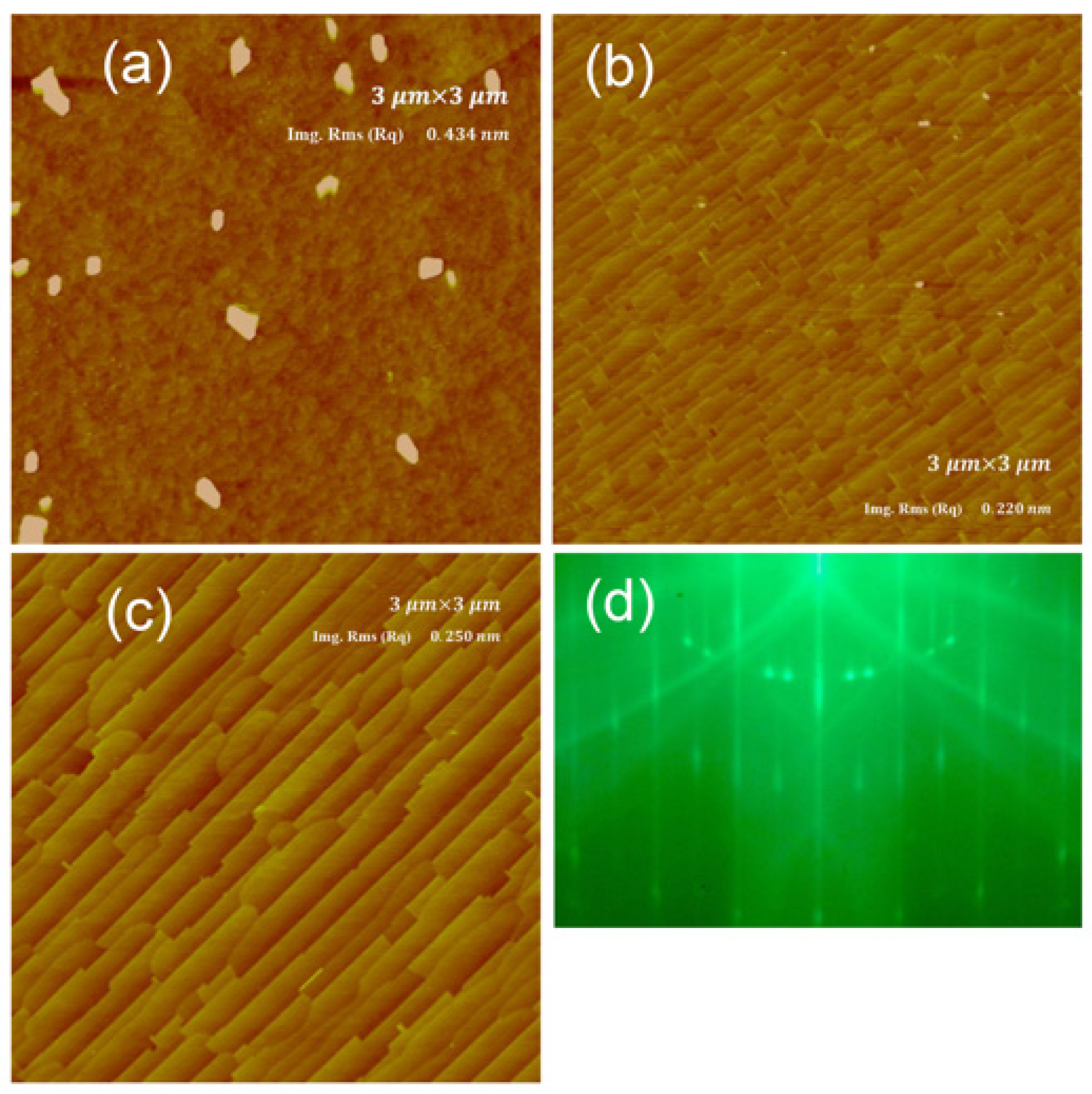
2.1. SrTiO3 (STO) Preparation and Characterization

Single crystal STO is one of the frequent substrate choices. It has a lattice constant of α = 3.905 Å, 3% larger than in an optimally doped LSCO (x = 0.16), which has α = 3.777 Å. The nearly matching lattice constant makes STO a good template for the LSCO film growth. The substrate’s quality, especially surface perfection, is essential for successful film growth.
We use 10 × 10 × 1 mm3 single-crystal STO substrates with one-side epi-polished perpendicular to the [001] direction and the other side sand-polished. MTI Corporation manufactures the substrates. We use a two-stage cleaning and annealing procedure to treat the STO substrates to obtain a clean, single-TiO2 termination surface [13]. We use AFM to study and monitor the quality of the substrate surface. A typical as-received STO substrate has a relatively rough surface with impurities and defects, as shown in Figure 2a. We clean the substrates with de-ionized water in an ultrasonic bath for 30 s and then anneal them in air, at 1000 °C, for one hour. After this treatment, an AFM image of the surface is shown in Figure 2b. Atomic steps can be seen, and there is a significant decrease in the abundance of defects on the surface. The RMS surface roughness is reduced from 0.43 nm to 0.22 nm. The substrate is washed with water in the ultrasonic bath for 30 s, followed by another one-hour annealing process, in the air, at 1100 °C. An AFM image of the surface, taken after this step, shows the broadening of the atomic steps on the substrate surface. The RMS roughness remained similar after the first washing and annealing process; however, the precipitates disappeared. The Reflection High-Energy Electron Diffraction (RHEED) pattern, Figure 2d, indicates the TiO2 surface termination of the processed substrate.

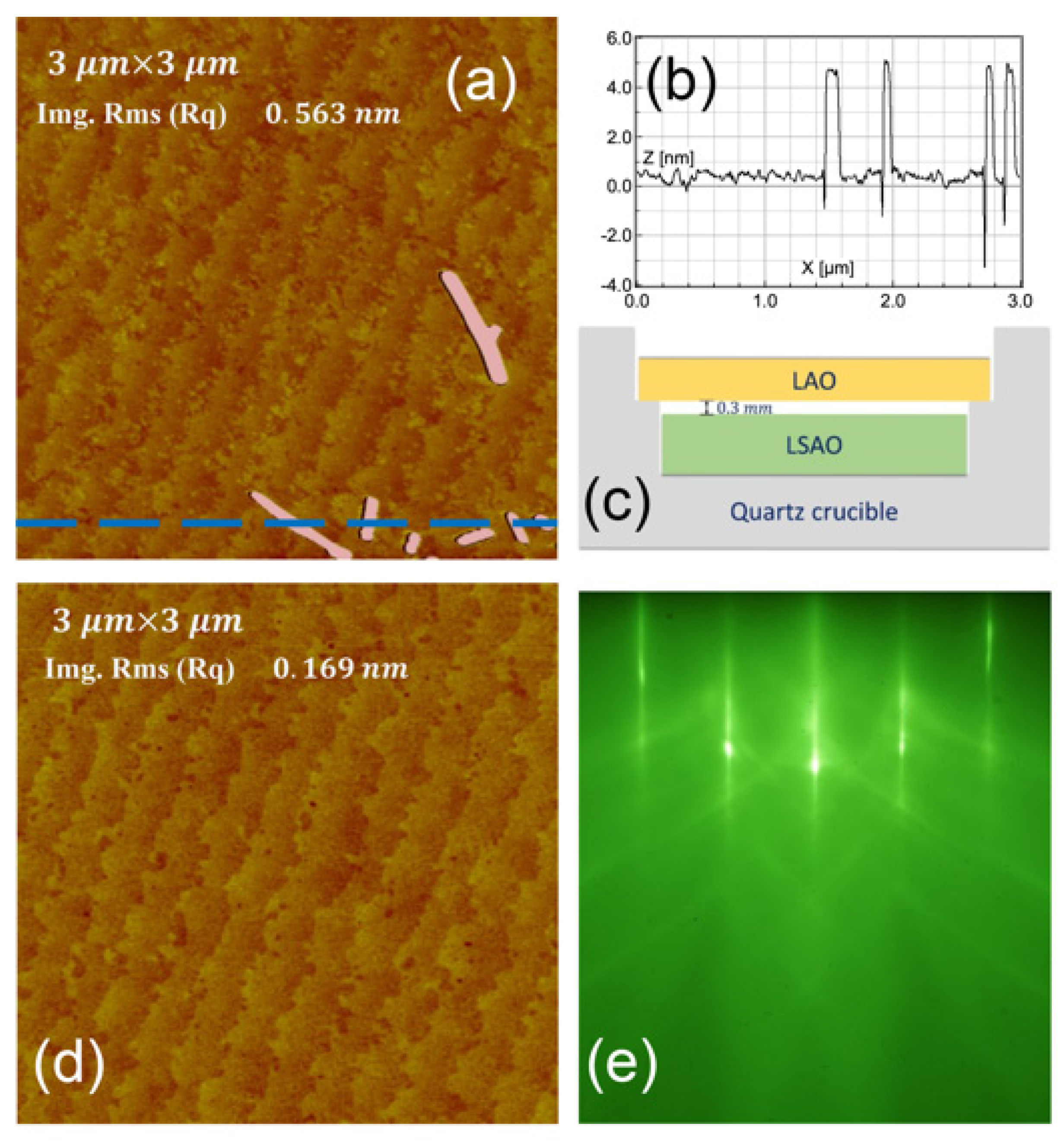
2.2. LSAO Preparation and Characterization

Single-crystal LaSrAlO4 (LSAO) substrates have a lattice constant of α = 3.755 Å, which is 0.5% shorter than in the optimally doped LSCO. The closely matched lattice constant and similar crystal structure make LSAO a perfect substrate for LSCO epitaxy. It also has an advantage compared to LaAlO3 (LAO); the LSAO substrates do not twin during heating and cooling.
For LSCO film synthesis, we preferably use a 10 × 10 × 1 mm3 LSAO single-crystal substrate supplied by MTI Corporation. One side of the substrate is epi-polished, while the other is sand-polished. We inspect each substrate by AFM. A typical as-received substrate may have defects on the surface, as shown in Figure 3a,b. To improve the surface, we soak the substrates in deionized water with resistivity > 18 MΩ, in an ultrasonic bath, for 30 s. Then, the substrate is rinsed with ethyl alcohol and dried immediately with dry nitrogen gas. The substrate is subsequently placed in a custom-built sapphire crucible face-to-face with a slightly larger LAO substrate, as shown in Figure 3c. The crucible ensures that the gap between the surface of the LSAO substrate and the LAO substrate is kept at 0.3 mm. The setup is annealed in a tube furnace at 950 °C, in the air, for 1 h. An AFM image of the processed substrate surface is shown in Figure 3d. The cleaning and annealing process removes the defects on the surface of the substrate and improves the atomic steps. The water dissolves the SrO precipitates during the cleaning, and the LAO substrate provides a cation-rich environment during the annealing process to suppress the formation of new SrO precipitates [14].

2.3. Backside Coating with SrRuO3

Our ALL-MBE system uses multiple quartz heater lamps with parabolic mirrors to ensure homogenous heating without using silver paste or paint. Most of our substrates, i.e., LSAO and STO, are transparent. To absorb the radiation from lamps, we coat the backside of the substrates with SrRuO3 (SRO). There are several reasons for this choice. Firstly, it is black in color to absorb radiation well. Second, it has high thermal conductivity, thus ensuring temperature homogeneity. Third, it is very stable at high temperatures and in an ozone environment. We deposit the SRO backside coating using radio-frequency sputtering. The substrate surface is protected by another substrate with a gold gasket sandwiched between them. This ensures that SRO does not contaminate the epi-polished surface of the substrate on which the LSCO film will be deposited later. During SRO sputtering, the substrates are kept at 650 °C, under a 100 mTorr partial pressure of Ar and 33 mTorr of O2. The sputtering power is purposely kept low, at 30 W, for four days, and at 40 W, for another four days. The slow (low-power, long-time) sputtering helps SRO stick better onto the backside of the substrate. This reduces peeling off the backside coating during heating in MBE growth.

3. All-MBE Technique
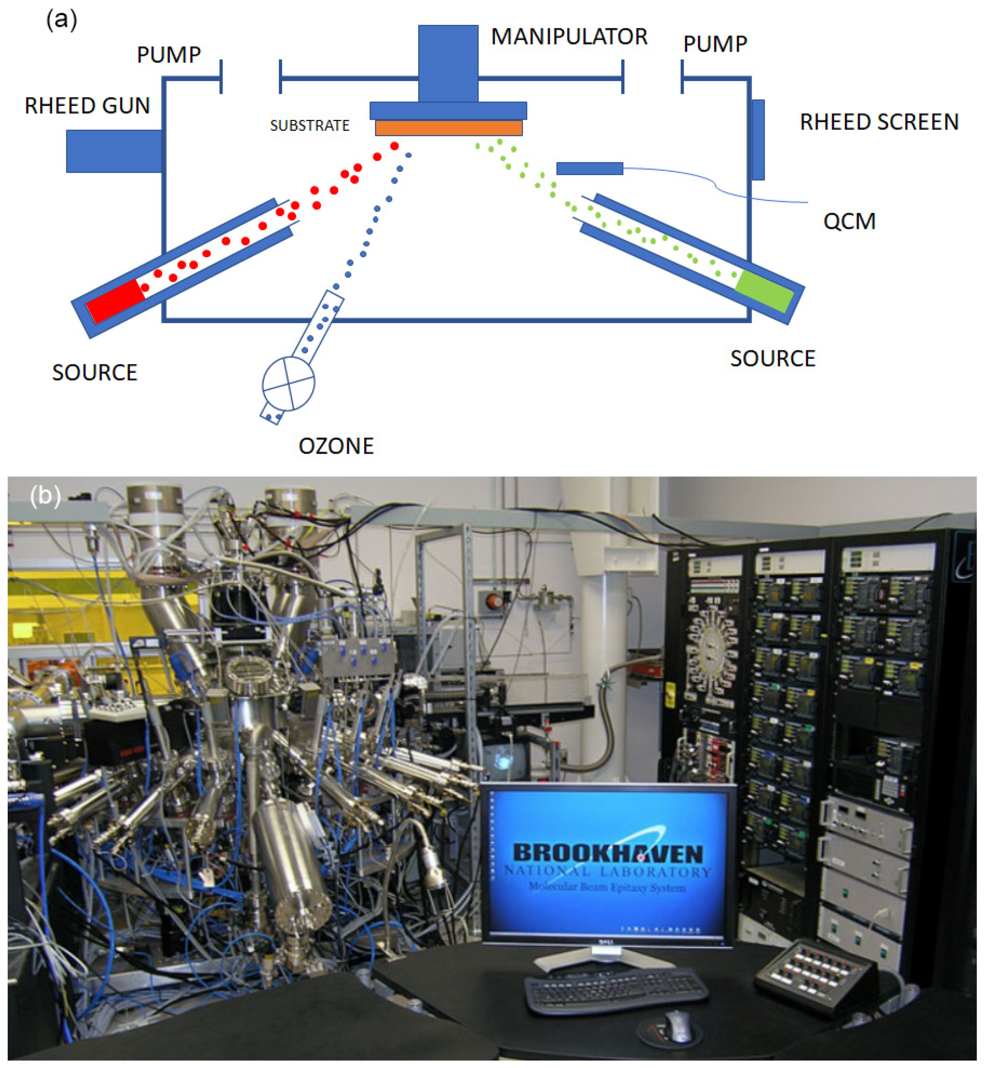
3.1. MBE System

Our ALL-MBE system (Figure 1b) is a multi-chamber ultra-high vacuum (UHV) apparatus that was custom-designed to synthesize superconducting oxides. The design is entirely modular; the system is divided into multiple autonomous subsystems, each pumped independently by its dedicated pumps. Hence, each subsystem can be independently vented for repair and maintenance. This dramatically increases the overall uptime of the whole system and its productivity. The system has 16 thermal evaporation sources and a pure ozone source. The sources are aimed at the substrate at a shallow incident angle (20°). We usually operate them in pairs because each source, when working alone, produces a gradient of the deposition rate, with a 4% difference across a distance of 10 mm. Two evaporators facing each other with the same source material can compensate for this gradient and produce a homogenous and uniform film. However, we can also synthesize films deliberately designed to have a gradient of doping for combinatorial-spread experiments.
The ALL-MBE also has several in situ analytical tools, including a scanning quartz crystal microbalance (QCM), a double-deflection RHEED system, a time-of-flight ion-scattering-and-recoil spectroscopy (TOF-ISARS) system [9].

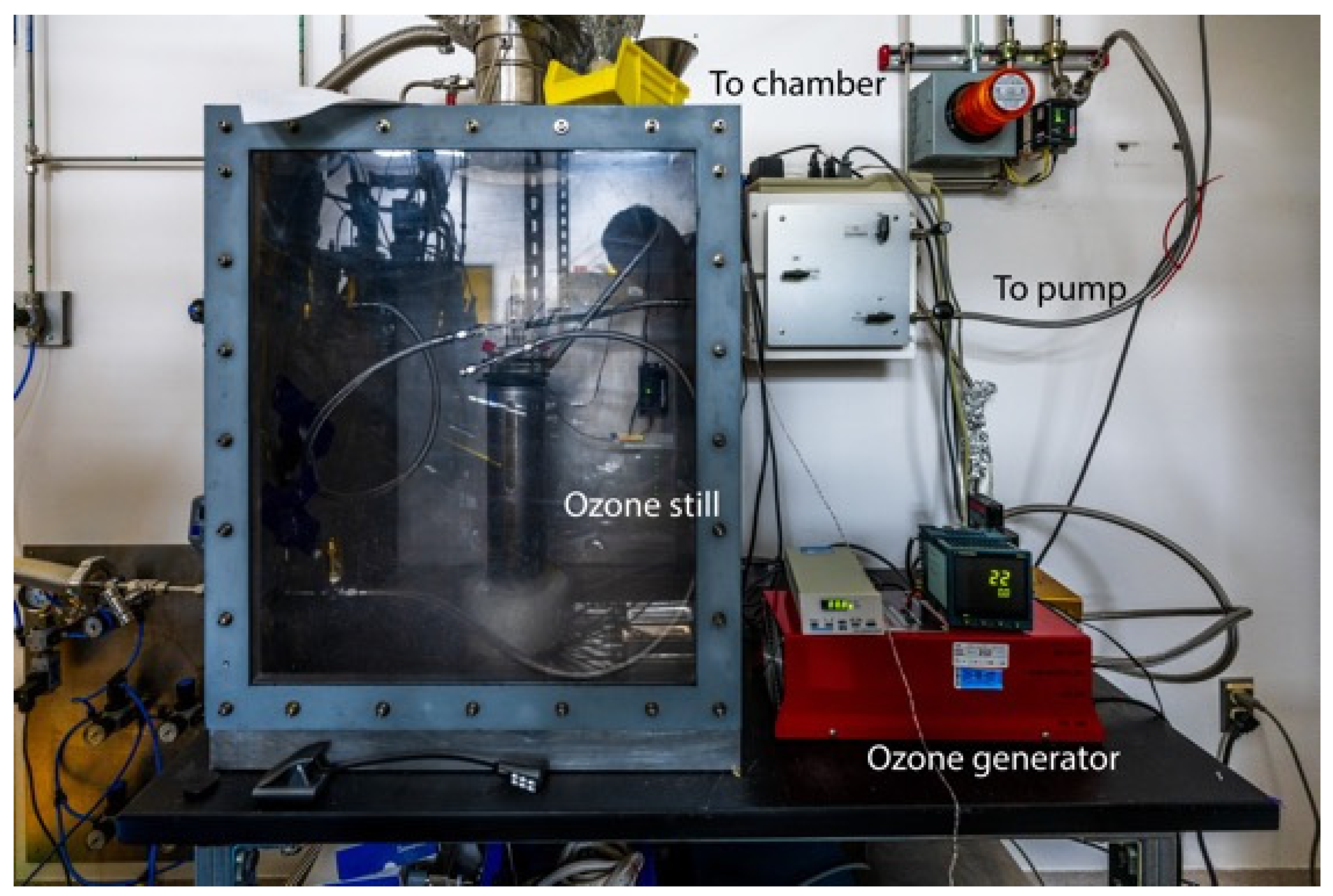
3.2. Ozone Distilling

Our ALL-MBE system uses pure ozone (O3) to oxidize metals. Copper is difficult to oxidize, so we need high oxidation power. On the other hand, we also need a relatively high vacuum to reduce the scattering of metal atoms in the beams emanating from thermal sources. To meet these competing requirements, we choose ozone gas as our oxidizer since it has several orders of magnitude higher oxidation power than the commonly used oxygen gas (O2). To produce pure ozone, we designed an ozone distillation system photographed in Figure 4. In the first step, a commercial ozone generator produces some O2:O3 mixture out of pure oxygen gas. The mixed gas is then liquefied in a zone-condenser vessel cooled by liquid nitrogen. The temperature of the vessel is controlled by a heater and kept at around −165 °C. At this temperature, trace compounds like water vapor and CO2 are in solid form and fall to the bottom of the vessel, while O2 and traces of N2 are still in the gas form and are pumped out quickly. What remains above the liquid is a pure ozone vapor, the pressure of which can be controlled by adjusting the pumping speed and temperature. We use a water-cooled stainless steel tube with a needle valve to feed ozone into the chamber. The ozone partial pressure in the MBE synthesis chamber is maintained by a closed proportional-integral-derivative (PID) control loop by heating the liquid ozone vessel and vaporizing the liquid ozone.

3.3. Substrate Temperature

The MBE synthesis chamber has a two-wavelength pyrometer and a digital camera mounted on a custom-designed remotely-controlled rail slider. The slider can move the pyrometer and the digital camera so that one aims at the sample. We use the digital camera to monitor the position of the sample, aiding the sample-holder transfer. The pyrometer monitors the temperature of the substrate to an accuracy of 0.1 °C.

3.4. Source Calibration

To accurately measure the actual deposition rate on the substrate, a QCM sensor is mounted on a motorized UHV linear transfer arm so that it can be moved to the exact location of the substrate. During the calibration, the quartz sensor is temporarily moved to the precise position where the substrate is kept during the film growth while the substrate holder is moved up and out of the way. A cup is mounted at the back of the QCM sensor to protect the substrate from unintended deposition during calibration. The total deposition rate of each Knudsen cell is measured to the accuracy of <0.0003 atomic layers (AL) per second. During the calibration, ozone is delivered into the chamber to ensure that the materials deposited on the quartz sensor are oxides, the same as in the actual film. The partial pressure of ozone is kept the same as during the sample growth because it affects the actual deposition rate due to scattering. We perform the detailed source calibration before each film growth to prevent flux drifting due to the depletion of the source material. To maximize the growth-to-growth reproducibility and ensure the correct timing, we keep the deposition rates for each element as constant as possible: the SrO rate at 0.005 AL/s, and the La2O3 and CuO rates are kept at 0.010 AL/s.

4. Synthesis of LSCO Films on LSAO Substrates

4.1. Buffer Layer

Buffer layers are commonly utilized for thin film growth, especially in MBE synthesis practice. For LSCO growth, we use one or two MLs of highly overdoped LSCO (x = 0.40) as a buffer layer before depositing other LSCO compositions. These overdoped LSCO layers can accommodate the lattice (crystallographic) and electrostatic (“polarization catastrophe”) mismatch between the desired LSCO sample and the substrate. It seems metallic and overdoped LSCO can self-arrange itself to accomplish this goal, resulting in a more perfect crystal structure in the intended LSCO [15,16,17].

4.2. Film Growth

LSCO has a layered-perovskite structure. It consists of a CuO2 layer sandwiched between two La-O layers (with Sr substituting for some of the La atoms). Two (La, Sr)-O layers and one layer of CuO2 layers make up one ML, and two MLs make up one unit cell. One ML is about 6.6 Å thick, and one unit cell is 13.2 Å wide, which is the height c0 of the unit cell. In our MBE, we grow these ML structures one by one. This is achieved by controlling the deposition of each element with a computer-controlled pneumatic shutter. We deposit the desired amount of La and Sr to 2ML thickness, then 1ML of Cu. The deposition is carried out in ozone, so the metals are all oxidized into the respective oxides. The LSCO film is epitaxially anchored to the substrate and follows the crystal structure of LSAO. The substrate temperature is kept at around 630 °C. We typically use slightly lower temperatures for overdoped LSCO and slightly higher temperatures for underdoped LSCO films. The background ozone partial pressure in the MBE chamber is kept at 1.0 × 10⁻⁵ Torr. The shutters for La and Sr cells open first for a certain amount of time, typically about 200 s, with the exact number adjusted based on the calibration of each cell. After the cells close, we wait for 20 s for the atoms to diffuse and migrate into their desired locations. Then we open the shutters for the copper cells for the time intervals based on their calibrations. After copper deposition, the RHEED pattern initially becomes sharper but saturates after a while. So, after the copper cells close, we wait for between 30 s to 5 min, depending on the evolution of the RHEED pattern.
We repeat this process until the intended number of MLs is deposited. Each ML takes 3–8 min, depending on the waiting time. Using ALL deposition, we can control precisely the number of MLs we grow and vary the doping within each ML. In addition, with the 16 sources we have in this MBE system, we can change the composition or different materials during a single growth session, providing much flexibility to fabricate artificial heterostructures, such as multilayer junctions and superlattices.

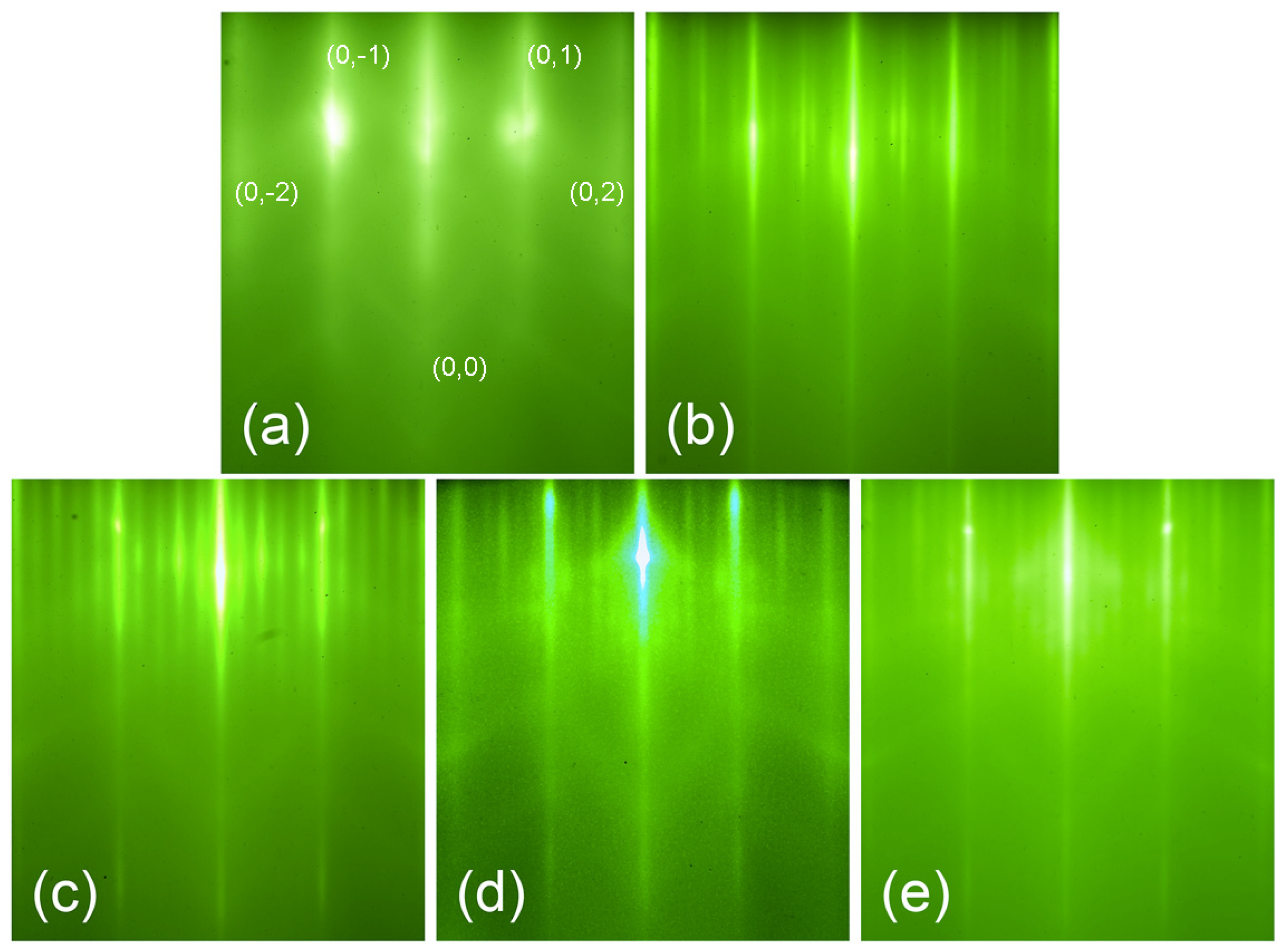
4.3. RHEED Monitoring

RHEED is a very surface-sensitive tool for in situ, real-time monitoring of the crystal structure of the film surface [18]. It also provides some information on the surface roughness and the sample morphology to differentiate between two-dimensional (2D) and three-dimensional (3D) growth. A typical RHEED pattern of the LSAO substrate is shown in Figure 5a. When the electron beam is aligned with the [100] direction of the substrate, it shows five main streaks. This RHEED pattern is characteristic of an atomically flat LSAO surface without any islands and precipitates. The streaks originate from the (0,−2), (0,−1), (0,0), (0,1), and (0,2) Bragg diffraction rods. The distances between the streaks in the k-space are proportional to the inverse of the lattice constant of LSAO, a0 = 3.755 Å. The RHEED images of our LSCO films (Figure 5b–d) show the same five main streaks at precisely the same spacing. Hence, we conclude that the in-plane lattice constant in these thin LSCO films is the same as in the LSAO substrate. The sharpness of the main streaks shows that our LSCO films also have a clean, highly crystalline, and atomically flat surface.
The RHEED images of our LSCO films also have one prominent feature absent in LSAO: multiple weaker satellite streaks (“sidebands”) positioned between the main streaks. These sidebands appear in LSCO films for all doping levels. The number of the sidebands N is determined by the superstructure due to surface reconstruction, with the supercell period N × a0 in real space. The number of sidebands varies with the doping level. Apart from the long and sharp main and sideband streaks, the RHEED images of our LSCO films also feature a very bright specular spot, visible diagonal (“Kikuchi”) lines, and Laüe-circle reflections. All these features are indications of the high crystallinity of the film.

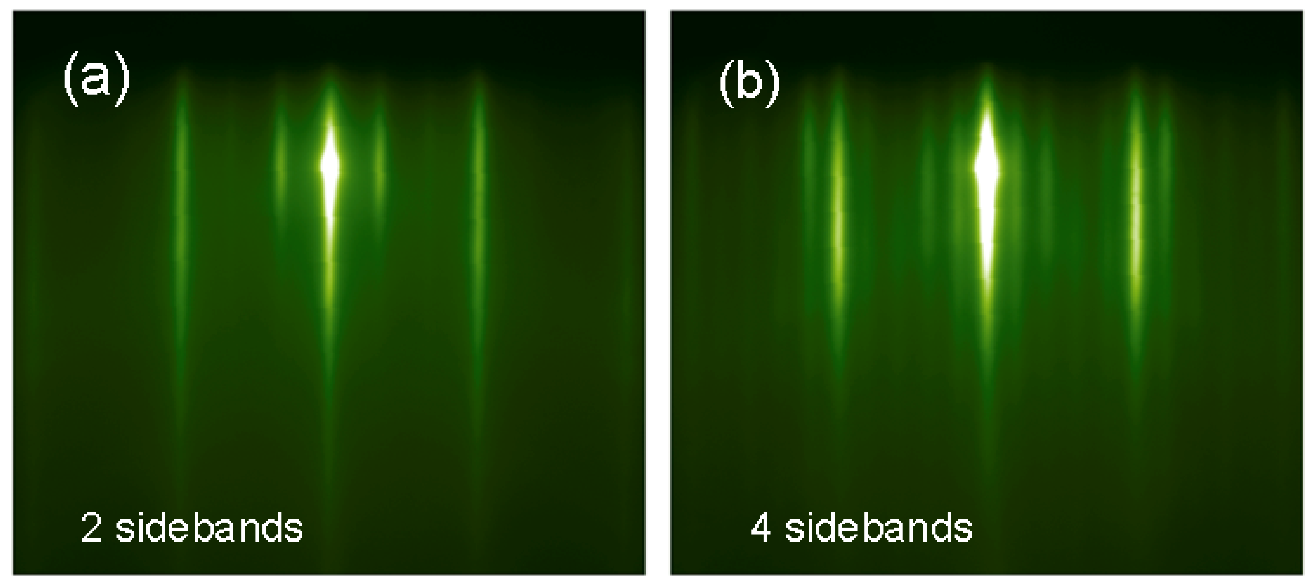
4.4. RHEED Dynamics as a Diagnostic Tool for Fine-Tuning the Stoichiometry

Cuprates or other complex oxides contain multiple elements. In general, it is not easy to maintain the correct stoichiometry of all the elements with any thin film growth technique. If one or more sources drift by a small amount over time, causing minor errors in the stoichiometry, secondary-phase precipitates can be generated during growth. These can be detected in RHEED images as spots due to the Bragg diffraction of the beam transmitted through nano-scale precipitates instead of streaks. Depending on which unwanted phase forms, these spots can appear at different locations in the RHEED images. In our case, these most likely phases are La2O3, SrO, or CuO. The spots due to La2O3, or SrO precipitates, appear inside the main streaks, while the CuO defects produce spots outside the main streaks. This is due to the lattice constant of La2O3 being larger and the CuO lattice constant being smaller than in LSCO. RHEED can detect such precipitates while still tiny, on the 10–20 nm scale, as these produce large (due to Scherrer broadening) spots in the RHEED pattern. When these defects are detected early enough, it may be possible to dissolve them by adjusting the stoichiometry of the film. These defects, especially CuO precipitates, can modify the film properties, including superconductivity, obscuring the intrinsic properties under study.
To maintain the correct stoichiometry, we developed a novel monitoring strategy by studying the RHEED patterns of LSCO films. As mentioned previously, the LSCO films show sidebands in the RHEED pattern, which evolve and change during the growth. By timing this evolution, we fine-tune the stoichiometry during growth by changing the deposition time of each element in real-time. For example, during the synthesis of the optimally doped LSCO, the sideband number varies from 2 to 4 when depositing the CuO layer shown in Figure 6a,b. We started the timer when the pattern transformed from 2 to 4 sidebands and stopped the timer when the copper deposition ended. We maintain a constant time of this surface transformation by fine-tuning the deposition time of copper element, and consequently, the correct stoichiometry is held.

4.5. Adjusting the Oxygen Stoichiometry

The actual chemical composition of LSCO is, in fact, La2−xSrxCuO4+δ, where δ can be positive, zero, or negative. The actual oxygen stoichiometry affects the mobile carrier density and the superconducting properties of LSCO. The undoped parent compound LCO and underdoped LSCO are more prone to intercalation of extra oxygen (i.e., δ > 0), which occupies sites interstitial between the two (La,Sr)O layers [19]. This tendency is enhanced due to the lattice mismatch of LSAO and LSCO. The LSAO substrate provides a compressive strain to the LSCO film, and the reduction of the in-plane lattice constants of LSCO causes the expansion c-axis lattice constant. The extra space makes it easier for additional oxygen atoms to occupy interstitial sites. This makes the LCO parent compound metallic and superconducting and increases the Tc of underdoped LSCO. On the other hand, the overdoped LSCO is prone to forming oxygen vacancies (δ < 0) for chemistry reasons. It is tough to oxidize copper to more than the (+2) state, while oxygen favors the closed-shell (−2) ionic state [20]. Oxygen vacancies strongly affect the conductivity in normal state and superconductivity of the LSCO [21].
To control δ, we are solving the problem in two separate processes. During growth, we adjust the oxidation power by changing the growth temperature. For underdoped samples, we use slightly higher growth temperatures, which provide less oxidation power according to the log(p)-1/T phase diagram plots, where p is the partial pressure of the ozone and T is the temperature of the substrate during growth [22]. When overdoped samples are synthesized, lower substrate temperatures increase the oxidation power. The range of the temperature is limited. Too high temperatures result in sample degradation, while low temperatures result in poor crystallinity. We have even less freedom to change the pressure. Too high pressure significantly increases the scattering of the molecular beam from the source and decreases the deposition rate. In addition, too high an ozone concentration could damage the RHEED gun and burn the source filaments. Our solution to this problem is post-growth annealing in situ at conditions that vary for different doping. Once the growth is finished, sensitive equipment can be switched and valved off, and more ozone can be leaked into the main growth chamber. In this situation, we have much more freedom in rising p, and T. Annealing at a high temperature improves the film crystallinity and makes the superconducting transition sharper. However, given the exponential character of the p–T dependence, this may reduce the oxidation power so that the sample loses oxygen even under a higher ozone pressure. Annealing at a temperature lower than the growth temperature under high partial pressure of ozone can dramatically increase the oxidation power, filling the oxygen vacancies. On the other hand, annealing in a vacuum at an appropriate lower temperature can extricate the interstitial oxygen atoms without removing the “structural” oxygen in the LSCO crystal structure.
Studying many films and testing different combinations was necessary to find the optimal temperature and ozone partial pressure. Over the last 20 years, after growing over 3000 LSCO films and studying them by various in situ and ex situ characterization methods, we developed a multi-step post-annealing in situ and ex situ procedure. For in situ annealing, after the growth is finished, we increase the partial pressure of ozone in the chamber to 1 × 10⁻⁴ Torr. For underdoped LSCO, we anneal the sample at 675 °C for 5 min, then at 610 °C for 30 min, under the same pressure. After that, the film is cooled in ozone, still under the same pressure, to 250 °C. Once the temperature stabilizes at 250 °C, the chamber is pumped down, and the sample is annealed in a high vacuum for 30 min. Finally, the sample is cooled, in a vacuum, to room temperature.
Optimally doped LSCO films do not need this vacuum-annealing process. They are heated to 675 °C, kept for 5 min, then cooled to 610 °C for 30 min, and then cooled down to room temperature under the ozone partial pressure p = 1 × 10⁻⁴ Torr during the whole annealing process.
Overdoped LSCO films lose oxygen easily, so we avoid high-temperature annealing in this case. Instead, they are annealed under the ozone partial pressure p = 1 × 10⁻⁴ Torr at T = 600 °C for up to 4 h and then cooled down in the same ozone environment to room temperature.

5. LSCO Film Characterization

After the film growth process, all our films are subject to a few ex situ tests to evaluate the film quality. In our experience, two of these tests are the most essential for LSCO films: AFM imaging and MI measurements [23]. From these two experimental probes, we can gauge the quality of the film, for example, whether there are defects on the film surface, whether the film has atomic steps that follow those in the substrate, what the Tc of the film is, and how uniform the superconducting transition is.

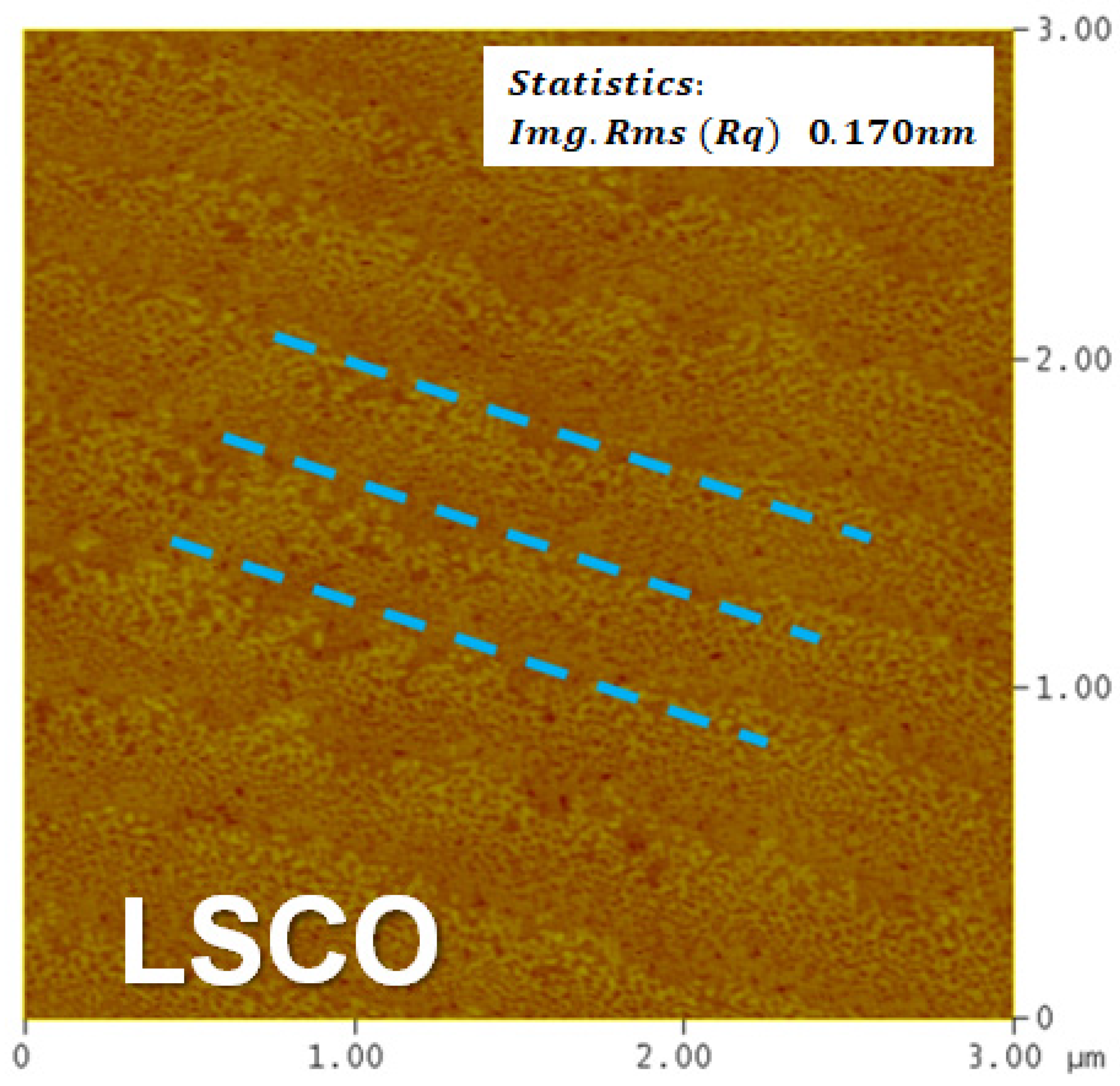
5.1. Atomic Force Microscopy

Figure 7 shows a typical AFM image of a good LSCO film synthesized by ALL-MBE on an LSAO substrate. We can see the atomic steps of the LSCO film, which follow the atomic steps of the substrate. These steps occur because of an inevitable slight miscut during the manufacturing process (typically 0.1°–0.5°) away from the ideal crystal plane perpendicular to the [001] direction of the substrate. These terraces are one ML tall, and the terraces between two steps are essentially atomically flat. The overall RMS surface roughness is 0.17 nm, which is less than the height of one ML (0.66 nm).

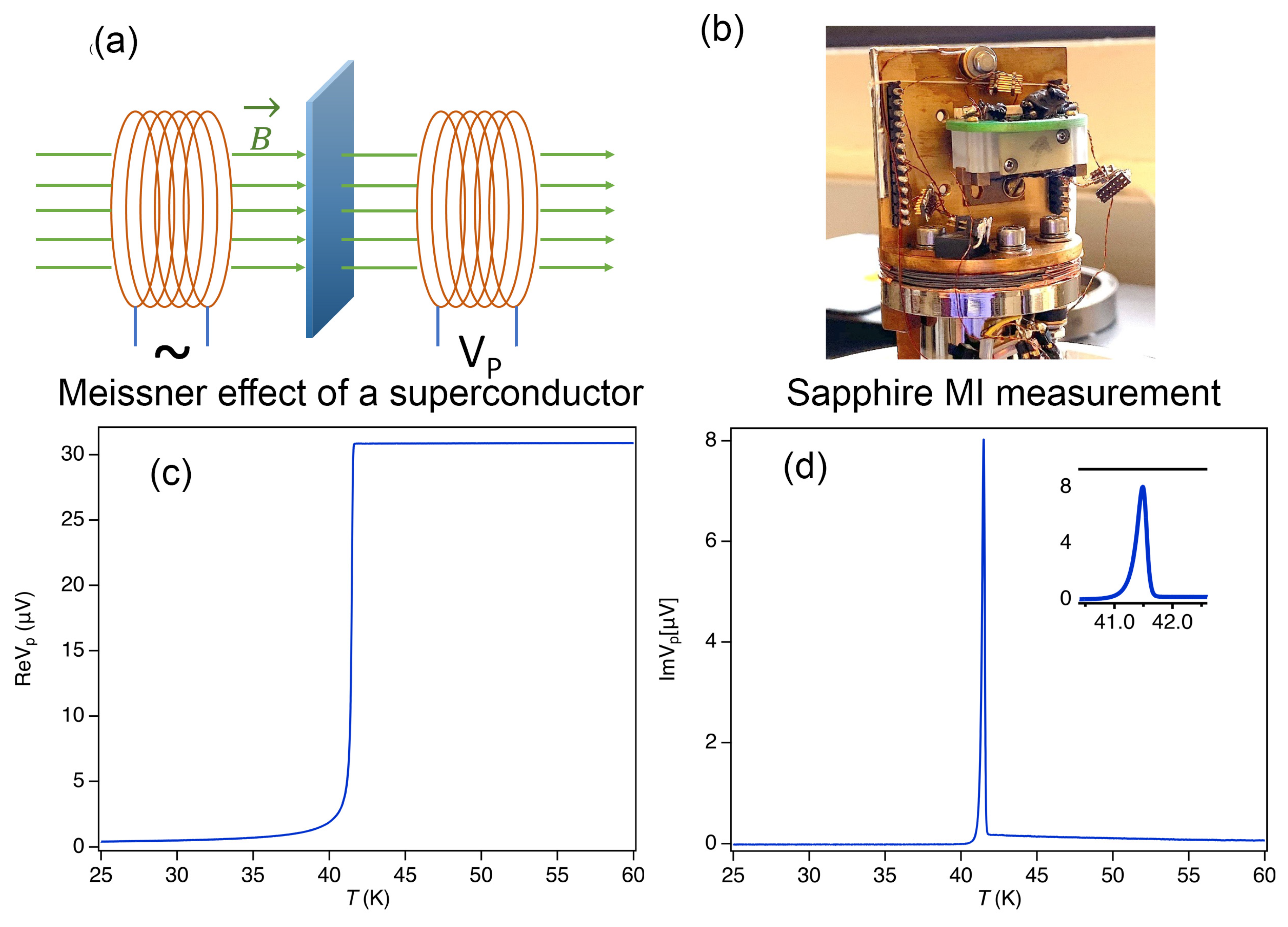
5.2. Mutual Inductance

MI is one of the best tools for studying superconducting films. The principle of the MI experiment is straightforward. A drive coil and a pickup coil are aligned with one another, forming a mutual inductor, as shown in Figure 8a. The MI can be measured as the real part of the electromagnetic field (emf.) generated in the pickup coil when an alternating current flows through the drive coil. When the superconducting film is placed between the drive and pickup coil, the MI signal can be significantly altered once the film becomes superconducting due to the diamagnetic screening (the Meissner effect) in the film. The real part of the emf is proportional to the MI, while the imaginary part is proportional to the AC conductivity.
If the MI apparatus, shown in Figure 8b, is manufactured precisely, with all the aspects—electronic, mechanical, and thermal, the geometry of the coils and films, etc.—tightly controlled, the MI signals are very reproducible, within a fraction of percent. In this case, the penetration depth λ and the AC conductivity can be derived from the complex impedance with remarkable absolute accuracy (better than 1%). The MI data of a typical well-grown LSCO film are presented in Figure 8c,d. One can read Tc from the onset of the Meissner effect, i.e., the drop in ReVp(T), see Figure 8c, and equivalently from the onset of the sharp rise in ImVp(T), see Figure 8d. These changes in MI coincide with the vanishing of the resistivity in the film.
More importantly, from these data, we can also evaluate how homogeneous the film is. If the film had two or more large domains with two or more values of Tc that differed by more than one half-width-at-half-maximum (HWHM) of one peak in ImVp(T), we would resolve two or more distinct peaks. Hence, the sharper the peak, the more homogeneous the film must be. In the LSCO film illustrated in Figure 8c,d, the variations in Tc are less than 0.2 K over the 10 × 10 mm2 area, which means that the whole film transitions to the superconducting state at the same temperature. This is also a testimony to the quality of this film.

6. Conclusions

We grew LSCO thin films using an ALL-MBE system specially designed to synthesize HTS cuprate materials, using pure ozone as the oxidizer. The experience we accumulated by producing over 3000 films within 20 years enabled us to formulate a detailed recipe for growing atomically flat single-crystal LSCO thin films without any pinholes and secondary-phase precipitates. The timing and diagnostics based on the dynamics of the RHEED images help us fine-tune the stoichiometry of the metal elements within each layer. The muti-step in situ post-growth annealing allows us to adjust the film’s oxygen stoichiometry. Real-time RHEED and ex situ methods such as AFM and MI help us check the quality of the films and, in turn, to find and refine the recipe over the years. High-quality LSCO films have enabled many fundamental studies of HTS cuprates. The high purity and uniformity of the films combined with the extensive statistics allow us to discern the intrinsic properties of LSCO.
Furthermore, our ALL-MBE system and technique allow us to fabricate complex heterostructures, interface superconductors, trilayer junctions, and artificial superlattices. The knowledge and experience gained from LSCO synthesis also apply to other complex oxide compounds. It can speed up finding and fine-tuning the recipes to grow other complex oxide materials. It may open new fields of research and reveal new physics.

Author Contributions

X.H. and I.B. conceived the thin film synthesis schemes. X.H. and X.X. synthesized films and performed AFM and MI measurements. I.B. and X.S. supervised the project. All authors discussed the results and contributed to the final version of the manuscript. All authors have read and agreed to the published version of the manuscript.

Funding

This research was supported by the DOE, Basic Energy Sciences, Materials Science and Engineering Division. X.H. was supported by the Gordon and Betty Moore Foundation’s EPiQS Initiative through Grant No. GBMF9074.

Institutional Review Board Statement

Not applicable.

Informed Consent Statement

Not applicable.

Data Availability Statement

All data are available upon reasonable request.

Conflicts of Interest

The authors declare no conflict of interest.

References

  1. Bednorz, J.G.; Müller, K.A. Possible HighTc Superconductivity in the Ba-La-Cu-O System. Z. Phys. B-Condens. Matter 1986, 64, 189–193. [Google Scholar] [CrossRef]
  2. Anderson, P.W. The Resonating Valence Bond State in La2CuO4 and Superconductivity. Science 1987, 235, 1196–1198. [Google Scholar] [CrossRef] [PubMed]
  3. Chen, Q.; Stajic, J.; Tan, S.; Levin, K. BCS–BEC Crossover: From High Temperature Superconductors to Ultracold Superfluids. Phys. Rep. 2005, 412, 1–88. [Google Scholar] [CrossRef] [Green Version]
  4. Zaanen, J.; Chakravarty, S.; Senthil, T.; Anderson, P.W.; Lee, P.; Schmalian, J.; Imada, M.; Pines, D.; Randeria, M.; Varma, C.; et al. Towards a Complete Theory of High Tc. Nat. Phys. 2006, 2, 138–143. [Google Scholar] [CrossRef]
  5. Lee, P.A.; Nagaosa, N.; Wen, X.-G. Doping a Mott Insulator: Physics of High-Temperature Superconductivity. Rev. Mod. Phys. 2006, 78, 17–85. [Google Scholar] [CrossRef]
  6. Laughlin, R.B. Fermi-Liquid Computation of the Phase Diagram of High- T c Cuprate Superconductors with an Orbital Antiferromagnetic Pseudogap. Phys. Rev. Lett. 2014, 112, 017004. [Google Scholar] [CrossRef]
  7. Keimer, B.; Kivelson, S.A.; Norman, M.R.; Uchida, S.; Zaanen, J. From Quantum Matter to High-Temperature Superconductivity in Copper Oxides. Nature 2015, 518, 179–186. [Google Scholar] [CrossRef]
  8. Eckstein, J.N.; Bozovic, I. High-Temperature Superconducting Multilayers and Heterostructures Grown by Atomic Layer-By-Layer Molecular Beam Epitaxy. Annu. Rev. Mater. Sci. 1995, 25, 679–709. [Google Scholar] [CrossRef]
  9. Bozovic, I. Atomic-Layer Engineering of Superconducting Oxides: Yesterday, Today, Tomorrow. IEEE Trans. Appl. Supercond. 2001, 11, 2686–2695. [Google Scholar] [CrossRef]
  10. Naito, M.; Sato, H.; Yamamoto, H. MBE Growth of (La,Sr)2CuO4 and (Nd,Ce)2CuO4 Thin Films. Phys. C Supercond. 1997, 293, 36–43. [Google Scholar] [CrossRef]
  11. Naito, M.; Sato, H. Stoichiometry Control of Atomic Beam Fluxes by Precipitated Impurity Phase Detection in Growth of (Pr,Ce)2CuO4 and (La,Sr)2CuO4 Films. Appl. Phys. Lett. 1995, 67, 2557–2559. [Google Scholar] [CrossRef]
  12. Locquet, J.-P.; Perret, J.; Fompeyrine, J.; Mächler, E.; Seo, J.W.; Van Tendeloo, G. Doubling the Critical Temperature of La1.9Sr0.1CuO4 Using Epitaxial Strain. Nature 1998, 394, 453–456. [Google Scholar] [CrossRef]
  13. Connell, J.G.; Isaac, B.J.; Ekanayake, G.B.; Strachan, D.R.; Seo, S.S.A. Preparation of Atomically Flat SrTiO3 Surfaces Using a Deionized-Water Leaching and Thermal Annealing Procedure. Appl. Phys. Lett. 2012, 101, 251607. [Google Scholar] [CrossRef] [Green Version]
  14. Biswas, A.; Rossen, P.B.; Ravichandran, J.; Chu, Y.-H.; Lee, Y.-W.; Yang, C.-H.; Ramesh, R.; Jeong, Y.H. Selective A- or B-Site Single Termination on Surfaces of Layered Oxide SrLaAlO4. Appl. Phys. Lett. 2013, 102, 051603. [Google Scholar] [CrossRef] [Green Version]
  15. Naito, M.; Yamamoto, H.; Sato, H. Intrinsic Problem of Cuprate Surface and Interface: Why Good Tunnel Junctions Are Difficult to Fabricate. Phys. C Supercond. 2000, 335, 201–206. [Google Scholar] [CrossRef]
  16. Nakagawa, N.; Hwang, H.Y.; Muller, D.A. Why Some Interfaces Cannot Be Sharp. Nat. Mater. 2006, 5, 204–209. [Google Scholar] [CrossRef] [Green Version]
  17. Pentcheva, R.; Pickett, W.E. Avoiding the Polarization Catastrophe in LaAlO3 Overlayers on SrTiO3 (001) through Polar Distortion. Phys. Rev. Lett. 2009, 102, 107602. [Google Scholar] [CrossRef] [Green Version]
  18. Bozovic, I.; Eckstein, J.N. Analysis of Growing Films of Complex Oxides by RHEED. MRS Bull. 1995, 20, 32–38. [Google Scholar] [CrossRef]
  19. Bozovic, I.; Logvenov, G.; Belca, I.; Narimbetov, B.; Sveklo, I. Epitaxial Strain and Superconductivity in La2−xSrxCuO4 Thin Films. Phys. Rev. Lett. 2002, 89, 107001. [Google Scholar] [CrossRef]
  20. Radaelli, P.G.; Hinks, D.G.; Mitchell, A.W.; Hunter, B.A.; Wagner, J.L.; Dabrowski, B.; Vandervoort, K.G.; Viswanathan, H.K.; Jorgensen, J.D. Structural and Superconducting Properties of La2−xSrxCuO4 as a Function of Sr Content. Phys. Rev. B 1994, 49, 4163–4175. [Google Scholar] [CrossRef]
  21. Leng, X.; Božović, I. Controlling Superconductivity in La2−xSrxCuO4+δ by Ozone and Vacuum Annealing. J. Supercond. Nov. Magn. 2015, 28, 71–74. [Google Scholar] [CrossRef]
  22. Hammond, R.H.; Bormann, R. Correlation between the In Situ Growth Conditions of YBCO Thin Films and the Thermodynamic Stability Criteria. Phys. C Supercond. Its Appl. 1989, 162–164, 703–704. [Google Scholar] [CrossRef]
  23. He, X.; Gozar, A.; Sundling, R.; Božović, I. High-Precision Measurement of Magnetic Penetration Depth in Superconducting Films. Rev. Sci. Instrum. 2016, 87, 113903. [Google Scholar] [CrossRef] [PubMed]
Figure 1. (a). Schematic of the MBE thin film deposition with ozone source as an oxidizer. (b). The ALL-MBE system in the Brookhaven National Laboratory.
Condensedmatter 08 00013 g001
Figure 2. STO substrate preparation. (a) AFM image of a typical STO substrate as received with large precipices on the surface. (b) STO substrate after the 1st cleaning and annealing process. A small amount of SrO out-diffusions is still presented as small white dots. (c) Substrate surface after the 2nd preparation process. The RMS roughness is 0.25 nm without visible out-diffusions. (d) RHEED image of the same substrate after the 2nd preparation process. Main streaks, Kikuchi lines, and signatures of TiO2 terminations can be seen.
Condensedmatter 08 00013 g002
Figure 3. LSAO substrate preparation. (a) AFM image of a typical as-received LSAO substrate with large particulates on the surface. (b) The AFM profile along the blue dash line in (a). The height of the particulates can be seen to be 5 nm. (c) The schematic of the LSAO annealing process face-to-face with an LAO substrate. (d) After the preparation, the AFM image of the same substrate with RMS roughness of 0.17 nm. (e) The RHEED image of the same substrate after the preparation process. Sharp main streaks and Kikuchi lines can be seen.
Condensedmatter 08 00013 g003
Figure 4. Photo of the ozone distillation system. A commercial arc-discharge ozone generator generates an ozone and oxygen gas mixture from a pure oxygen gas supply. The mixture is cooled in a quartz vessel (ozone still) with liquid nitrogen as a coolant. Then, the mixture is warmed up so that O2 evaporates and is pumped out, leaving a pure O3 liquid in the still. Ozone vapor is then supplied to the MBE growth chamber when needed. A PID-controlled heater controls the ozone vapor pressure.
Condensedmatter 08 00013 g004
Figure 5. RHEED patterns during the LSCO growth. (a) LSAO substrate. (b) Underdoped LSCO film (x = 0.14 in this case). (c) Optimally doped LSCO film. (d) Overdoped LSCO film (x = 0.24 in this case). (e) Heavily overdoped LSCO film (x = 0.30 in this case).
Condensedmatter 08 00013 g005
Figure 6. RHEED images of a typical optimally doped LSCO film. (a) After the (La, Sr)O layer. (b) After the CuO2 layer.
Condensedmatter 08 00013 g006
Figure 7. A typical AFM image of an LSCO film. The atomic steps are marked with blue lines, following the atomic steps of the substrate. The RMS surface roughness is 0.17 nm.
Condensedmatter 08 00013 g007
Figure 8. MI measurement of the LSCO films. (a) Schematics of the MI technique. (b) Photo of the actual MI system. (c) The real part of the Vp for an optimally doped LSCO film. (d) The imaginary part of Vp for the same film, the inset, shows the peak’s sharpness.
Condensedmatter 08 00013 g008
Disclaimer/Publisher’s Note: The statements, opinions and data contained in all publications are solely those of the individual author(s) and contributor(s) and not of MDPI and/or the editor(s). MDPI and/or the editor(s) disclaim responsibility for any injury to people or property resulting from any ideas, methods, instructions or products referred to in the content.

