1. Introduction
Random number generation is crucial for the security and applicability of cryptographic algorithms and protocols. In this sense, the generation of good random numbers has been a recurrent issue from the beginning of the development of secret- and public-key cryptosystems, and it has become critical nowadays due to the increasing computing power available to any attacker. From the initial development of computers, they have been a useful tool for generating such numbers, first for scientific and statistical uses [
1], and later for cryptographic purposes [
2]. Nevertheless, true random numbers cannot be generated by means of programming, and it is required to obtain entropy sources, initially from peripherals [
3] and later through the proposals of external hardware generators [
4]. Currently, computers make use of true random number generators (TRNGs) combined with deterministic random bit generators (DRBGs) included in external chips such as Trusted Platform Modules (TPMs) [
5,
6]. In the case of embedded systems implemented on reconfigurable logic, such as FPGAs or systems-on-chips, the usual solution is similar, combining a TRNG followed by a pseudorandom number generator (PRNG) (or a DRBG) in order to obtain a good trade-off between randomness, area resources, and power consumption [
7,
8]. In this sense, several designs of TRNGs [
9,
10,
11,
12,
13] and PRNGs [
14,
15,
16] to be implemented on FPGAs have been proposed. Among these proposals, those based on the use of ring oscillators (ROs) as sources of entropy combined with XOR gates to generate the final random bitstream seem to present the best statistical properties, although at the cost of high area requirements [
10]. In this work, we will analyze and propose some variants to these TRNG implementations that are suitable to be used in cryptographic applications on FPGAs, and we will provide a method to optimize the area and throughput of the implementation independently of the programmable device technology/manufacturer. The rest of the article is organized as follows:
Section 2 revises previous work in the literature regarding TRNGs implemented on FPGAs,
Section 3 provides the study of bitstream generation of basic sample ring oscillators, and
Section 4 revisits multiple XORed ring oscillators in order to achieve ultracompact TRNGs. Finally,
Section 5 compares these structures to other work in the literature, and the conclusions are provided in
Section 6.
2. Previous Work
The implementation of TRNGs requires sources of entropy as generators of randomness, along with a distillation process to avoid weaknesses in these sources. Taking into account the structure of FPGAs [
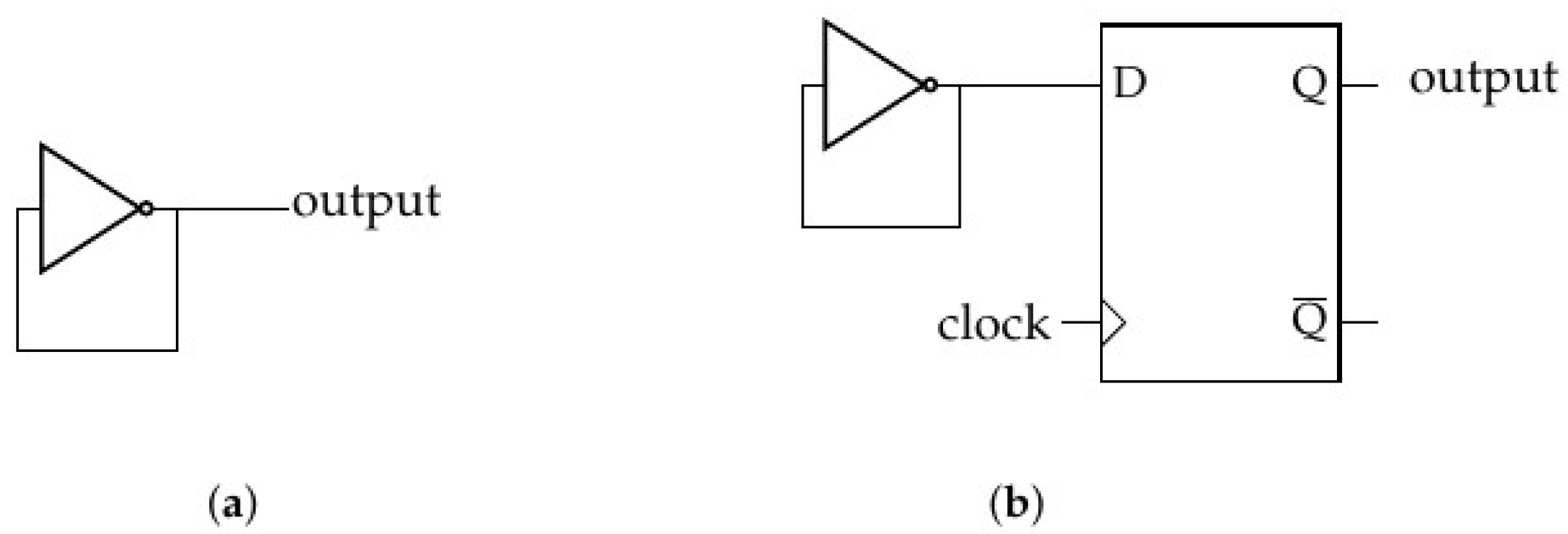
17], the sources of entropy are usually based on ROs. In this sense, a simple RO is built using one NOT gate, connected as in
Figure 1a. This feedback structure oscillates at a frequency that varies significantly depending on the process variations of the transistors in the cells where the ROs are placed when implementing the circuit [
18].
In [
19], a simplified model to estimate the delay of an RO is proposed:
where
is the average delay of the RO,
is the delay component due to process variations, and
is the delay component due to the noise generated in the logic element. Note that
depends on multiple factors, such as temperature, humidity, circuit activity, or side effects from the activity of neighboring cells. Therefore, this dynamic delay is the main source of the entropy originating from the RO. The values generated at the output of the RO need to be sampled to generate a random bitstream. The simplest method to perform this sampling is to place a flip-flop (FF) at the output, as shown in
Figure 1b, which corresponds to the so-called SRO-FF structure. In this case, the clock input of the FF acts as a sampling signal, at frequency
, being
. If the clock signal is decorrelated from the output of the RO,
presents enough variability (the other delays will remain relatively invariant, as the SRO-FF is implemented in only one logic element, LE), a random bitstream will be obtained. However, the variability of
may be not enough to avoid pattern repetitions due the periodicity of the clock and RO output signals. A proposal to overcome this issue is presented in [
20], where a second RO (RO2) is used to generate the sampling signal. The output signal of RO2 (
) feeds a frequency divider in order to maintain the relation
. This structure is known as ERO-TRNG [
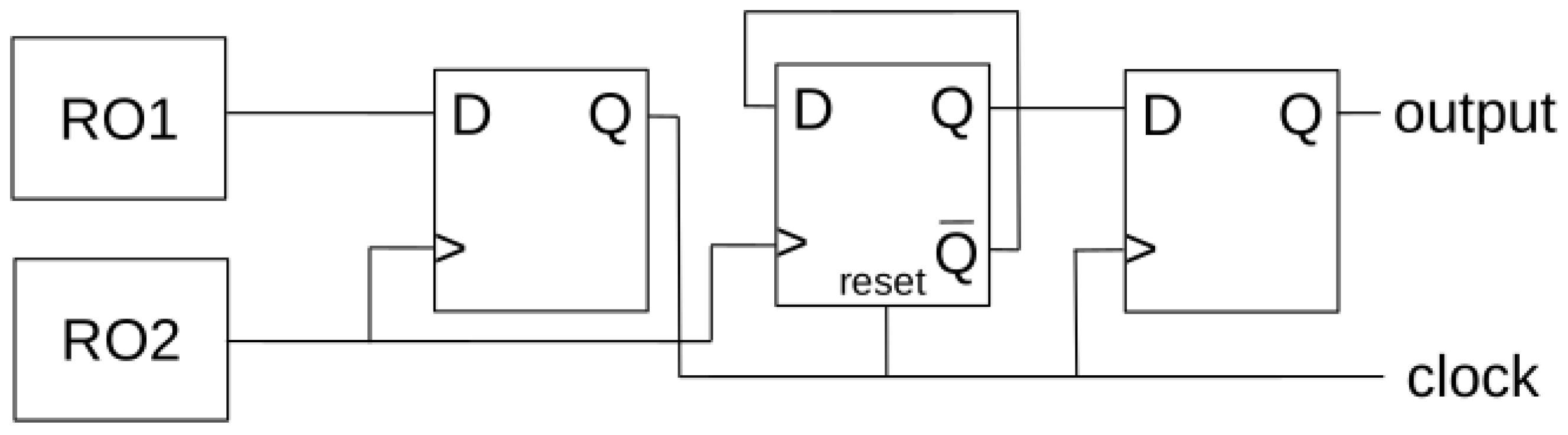
10], and it should be noted that it presents a limitation in the throughput of the RNG, as the output of the frequency divider is used as the clock signal for the system processing the bitstream. Another alternative consists of the structure shown in
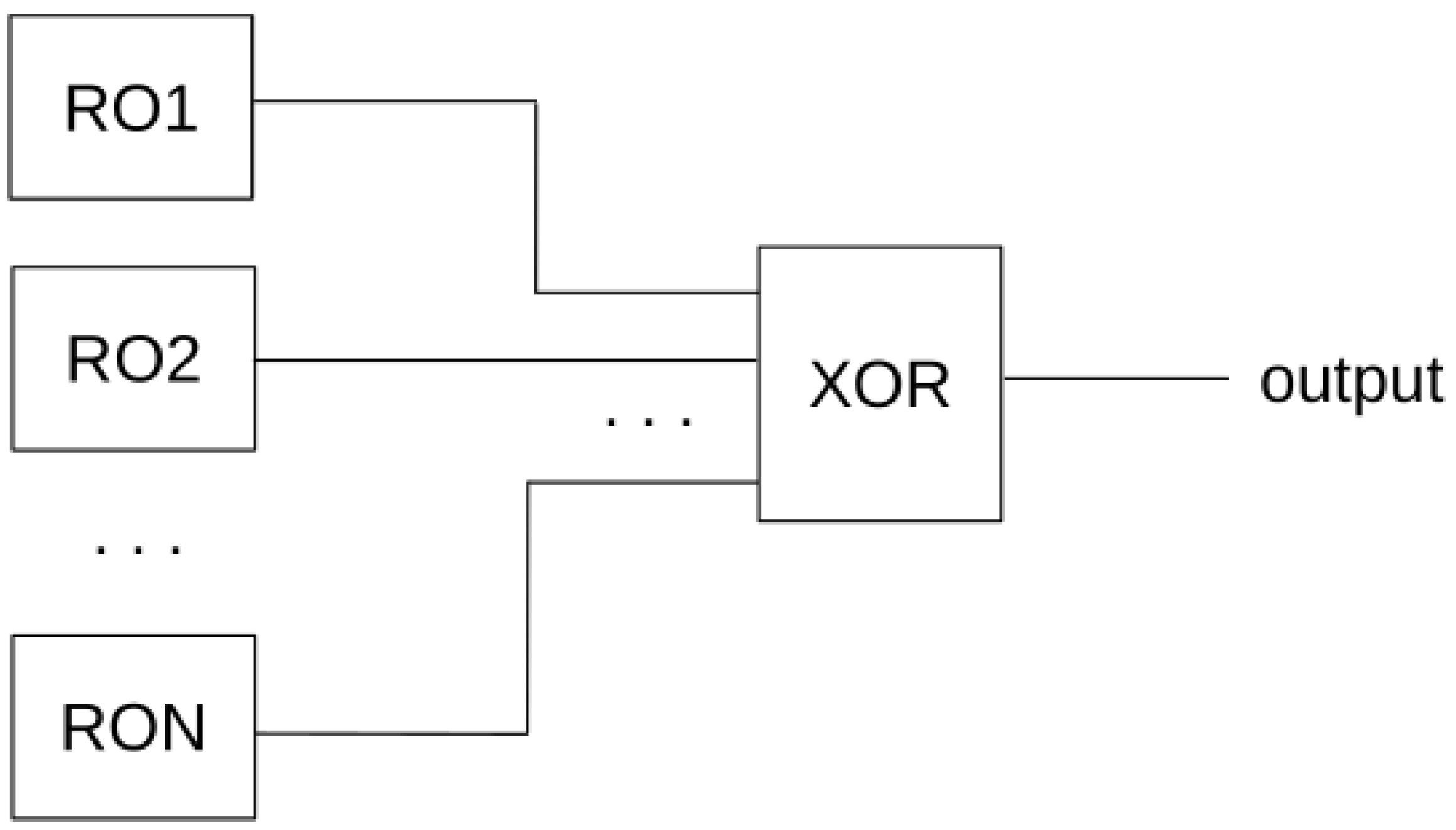
Figure 2, where the sampling clock signal is generated from two ROs [
21], but it has strict requirements in the maximum delay between the two RO feed signals, thus making it necessary to manually place and route them [
10]. The use of several ROs acting in parallel and feeding a XOR gate is proposed in [
22] and reproduced in
Figure 3. This is an interesting proposal, because the use of several ROs in parallel introduces more variability, as we will also have different
and
values for each RO. On the other hand, in [
23]; it is reported that a problem can arise if the XOR gate cannot change its output at the same rate that ROs are changing their states. In this same work, the introduction of a flip-flop between each RO and the input of the XOR gate, thus controlling the input rate to the XOR gate, is proposed to overcome this issue. Other solution was recently proposed in [
13], consisting of introducing a latch in the feedback path of each RO. Although these solutions introduce some limitations in the throughput, the additional variability provided by the parallelism of the structure enables compact implementations of TRNGs, as will be studied in
Section 4.
3. Study of a Basic Sampled RO
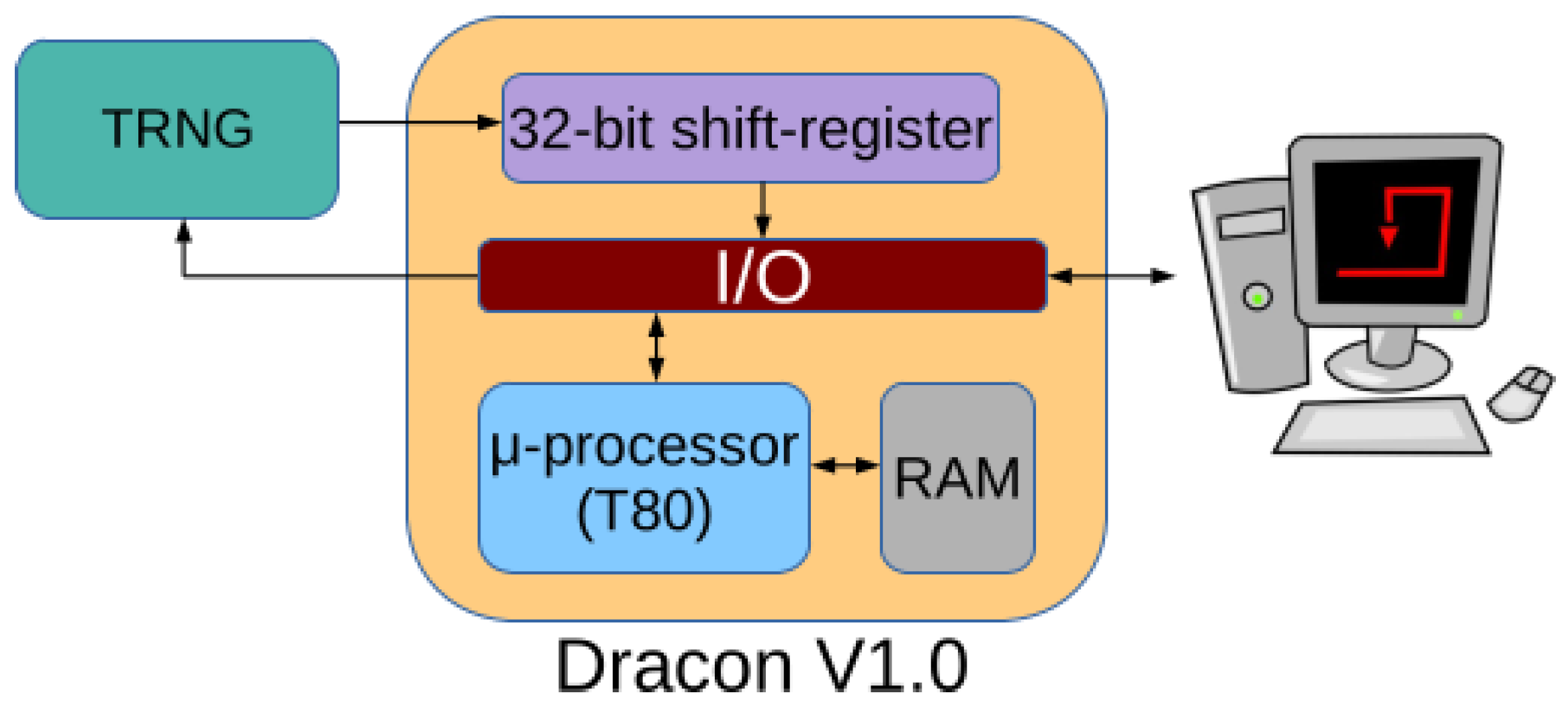
As a previous step to building compact TRNGs with multiple ring oscillators, we will carry out a detailed study of a basic RO sampled with a D flip-flop. As in the rest of studies presented in this work, the sampled outputs of the entropy source will be sent to a microprocessor-based platform, named Dracon [
24]. This platform is in charge of collecting and sending the generated numbers to a personal computer (PC) to be statistically analyzed, as shown in
Figure 4. Additionally, as the developed TRNGs are intended to be part of a more complex system integrated into an FPGA device, we will add an xenable input for switching off the RNG when it is not used, in order to reduce the power consumption. Indeed, in [
25], the high power consumption generated by ROs is shown, where they are even used to generate power noise or to extract information from the inside of FPGAs [
26]. The resulting structure is presented in
Figure 5, and it has a single source of entropy: an RO with two elements (the AND and NOT gates), a so-called SARO(1) (single-ANDed ring oscillator with 1 inverter). The complete structure is then named SARO(1)-FF. For our implementations, we used an Artix 7 device from Xilinx [
27], which includes six-input LUTs as basic logic elements, and the Vivado 2020.2 software. The exact device was an Artix 7 XC7A35T-1CPG236C on a Cmod A7-35T board from Digilent Inc., powered at 5 V from a laboratory power supply. All the experiments were carried out at a temperature of 26
C and a relative humidity of 33%. Since the objective was to achieve a compact TRNG with a reasonable throughput, a sampling frequency of
= 50 kHz was considered. Indeed, 50 Kbps suffices to generate the required random numbers in secure IoT applications or other cryptographic implementations over low-cost FPGA devices, and it implies a period long enough to accumulate the required jitter with a reduced number of inverting elements in the RO [
10]. In order to validate our results, we have generated a set of bitstreams and have analyzed the statistical properties for their use in cryptography by means of the SP 800-22 suite [
28], developed by the National Institute for Standardization (NIST). This suite includes a set of tests to analyze the randomness of bitstreams. The purpose, parameters, and interpretation of these tests are briefly described in the following [
29]:
Frequency test (Frequency): Analyzes the proportion of ‘0’s and ‘1’s for the entire sequence. This proportion should be 1/2, and each sequence to be tested should have bits.
Frequency Test within a Block (Block Frequency): Analyzes the proportion of ‘0’s and ‘1’s within M-bit blocks. In this case, n should be bits, and the block size M should be such that , , and , where .
Cumulative Sums Test (Cumulative Sums): This test analyzes whether the cumulative sum of the partial sequences occurring in the tested sequence is too large or too small relative to the expected behavior. This test has two modes, depending on whether it is applied forward or backward through the input sequence. In this test, n should be bits.
Runs Test (Runs): Analyzes the total number of “runs” in the sequence, where a run is a sequence of k identical bits. The purpose of this test is to determine whether the oscillation between ‘0’s and ‘1’s is too fast or too slow. The length of the sequence to analyze should be bits.
Test for the Longest Run of Ones in a Block (Longest Run): This test analyzes the longest run of ones within -bit blocks, thus determining whether the length of the longest “run” of ‘1’s within the tested sequence corresponds to what is expected in a random sequence. It uses three preset values for M in terms of the number of bits n of the sequence: when , when 750,000, and when 750,000.
Binary Matrix Rank Test (Rank): This test analyzes the linear dependence among fixed-length subsequences by determining the rank of disjoint submatrices of the entire sequence. The length of the sequence to analyze should be 38,912 bits.
Discrete Fourier Transform Test (FFT): This test detects periodic features in the sequence by applying the Discrete FFT. The length of the sequence to be analyzed should be bits.
Non-overlapping Template Matching Test (Non Overlapping): This test analyzes the number of occurrences of prespecified subsequences in order to detect too many occurrences of a given nonperiodic pattern. If the pattern is not found, the window slides one bit. For this test, the length of the templates should be or , and the length of the entire sequence, n, should be such that ( is recommended), , and .
Overlapping Template Matching Test (Overlapping): This test is similar to the previous one, but in this case, the window slides when the pattern is found. For this test, the length of the templates should be or , and the length of the entire sequence should be .
Maurer’s “Universal Statistical” Test (Universal): This test analyzes whether the sequence can be significantly compressed without loss of information. In that case, the sequence is considered not random. For this test, the sequence is divided into
L-bit blocks, recommended to be
, and
387,840. The concrete value of
L depends on
n, as specified in [
29].
Approximate Entropy Test (Approximate Entropy): This test analyzes the frequency of all possible overlapping -bit patterns across the entire sequence. For this test, n and should be such that .
Random Excursions Test (Random Excursions): This test analyzes the number of cycles having a given number of visits in a cumulative sum random walk. A cycle of a random walk consists of a sequence of random steps of unit length that begin at and return to the origin. This test is composed of a series of eight tests, and it requires .
Random Excursions Variant Test (Random Excursions Variant): This test analyzes the total number of times that a particular state is visited in a cumulative sum random walk. This test is composed of a series of eighteen tests, and it requires .
Serial Test (Serial): In this test, the frequency of all possible overlapping -bit patterns across the entire sequence is analyzed. n and should be such that .
Linear Complexity Test (Linear): In this test, linear-feedback shift registers (LFSRs) of length are built to check the linear complexity of the generated sequence. For this test, must be in the range of , and the length of the entire sequence should be .
Additionally, in [
29], it is established that the
p-value must be >0.01 to accept the hypothesis of randomness, and a minimum of “55 bitstreams should be processed to derive statistically meaningful results for the uniformity of
p-values”. Taking all of the above into account, we generated 125 bitstreams of 1,500,000 bits, each with the following set of values for the required parameters:
,
30,000,
,
,
,
,
.
Table 1 presents the results obtained for SARO(1)-FF, showing that it does not pass NIST tests when operating at a sampling frequency of
= 100 kHz. The limited variability introduced by only one RO and the high sampling frequency used produce a significant difference between the number of ‘1’s and ‘0’s generated, thus not passing the frequency-based tests. Moreover, a high sampling frequency generates a series of repeated ‘0’s and ‘1’s, thus not passing tests such as “Runs”. If we decrease the sampling frequency, it is possible to improve the test performance, thus obtaining the results in
Table 2 for
= 50 kHz.
The situation has thus been improved, but the asymmetry of the signal generated by a single RO makes it impossible to pass any frequency-based test. Moreover, the behavior of each RO depends on the process parameters of each transistor, which are different for each LUT used for its implementation and, of course, for each device. In this sense, we performed experiments with different placements in the same device, as well as using different devices, obtaining significant deviations in the probability of generating ‘0’s and ‘1’s by a SARO. These deviations sometimes imply
, and others
. The maximum deviation we measured for SARO(1)-FF at 50 kHz was
, i.e.,
, as shown in
Table 3. Note that since
,
. This deviation can be alleviated by using two SAROs in parallel and combining the two outputs by means of an XOR gate [
22], as will be studied in the next section. Regarding the number of inverting elements
k in a SARO(
k)-FF, we observed that SARO(0)-FF (just a NAND gate) provides bad results in terms of frequency tests due to the lack of stabilization of high and low levels at the NAND output. If the length is increased, the results in
Table 3 show better values for
, at the cost of a lower throughput (the oscillation frequency of the resulting RO is lower). In column
k, the type of gate used for enabling or disabling each RO (AND or NAND), as well as the number of NOT gates in the ROs, are specified in parentheses. Note that SARO(
k)-FF requires
LUTs and 1 FF to be implemented in an Artix-7 device, as pointed out in the LUTs+FF column in
Table 3.
On the other hand, at a sampling frequency of = 50 kHz, SARO(2)-FF or SARO(3)-FF do not present advantages with respect to SARO(1)-FF, thus SARO(1)-FF will be the basic RO that we will be consider for building multiple SAROs in order to carry out compact structures passing NIST tests.
4. Multiple XORed Ring Oscillators
As outlined in the previous section, asymmetry in the probabilities of obtaining a ‘0’ or a ‘1’ at the output of a SARO(
k)-FF can be compensated using an XOR gate. Indeed, if we consider a two-input XOR gate and let
and
be the probabilities of having a ‘0’ at inputs
and
of the XOR gate, respectively, while
and
are the probabilities of having ‘1’ at those same inputs, respectively, we find that the probabilities of obtaining a ‘0’ at the output will be
As an example, if
=
= 0.6, we will have
= 0.52, which improves the tendency of generating more ‘0’s than ‘1’s by the two SAROs feeding a 2-input XOR gate. The expected deviation is then
= 0.02, a
, which is excessive for passing any frequency test. In the case of considering a
N-input XOR gate, and assuming that
=
= ... =
, consequently (
=
= ... =
, and then the probability
can be computed as
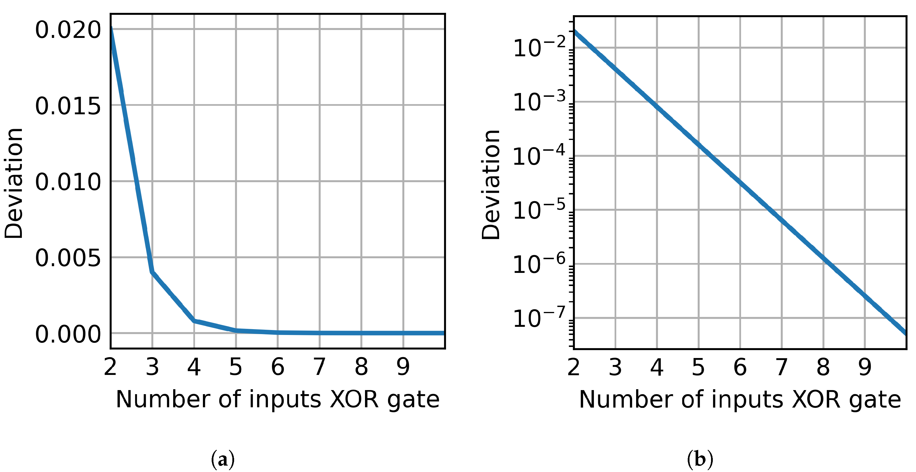
If we represent the deviation
as a function of
N for
, the graph in
Figure 6a is obtained.
Figure 6b presents the same graph, but in logarithmic scale, showing a clear linear relationship. As a consequence, it can be written as:
where
a and
b can be determined by linear regression or analytically. Indeed,
where
The exponential dependency of
with
N implies that an XOR gate with a high number of inputs (and therefore, a high number or SAROs) is not required to compensate for the generation probabilities of the ‘0’s and ‘1’s. The structure for building and testing such TRNGs for different values of
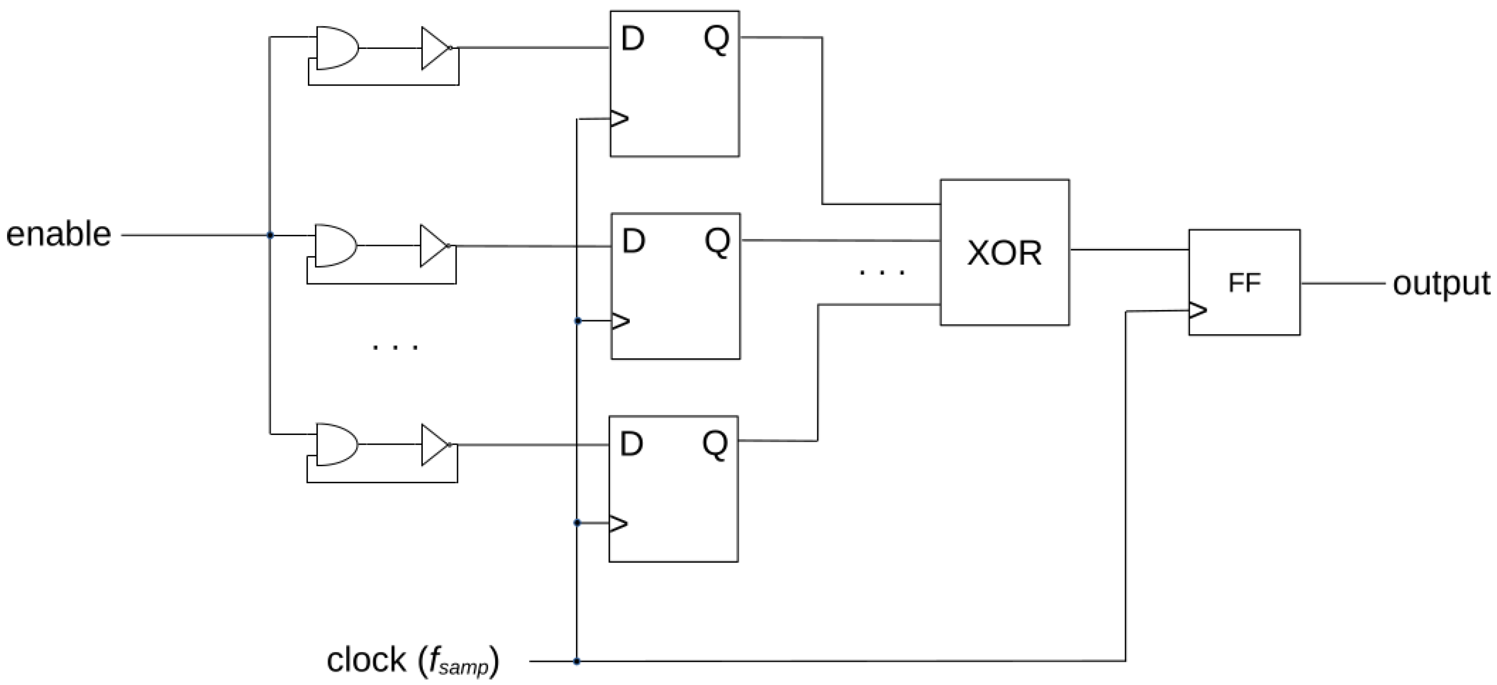
N is shown in
Figure 7. This structure is basically the one presented in [
10], where it is called MURO, and which, in turn, is based on [
22]. Only one difference is introduced: sampling is performed by a well-defined clock source instead of using a RO for this task, as in [
23] (however, this structure does not include the enable signal). Although it reduces variability at the output of the structure, it enables its behavior to be studied in terms of the sampling frequency.
Using this structure, which we have named Multiple XORed SARO(
k)-FF with
N ROs (MX-
N-SARO
), we performed the generation of bitstreams for different values of
N. In our experiments, the maximum deviation measured with a single SARO at 50 kHz was
, and in this case, theoretically, from Equations (
4) and (
6) for
, it would be
. However, the maximum measured deviation was
(
) at 50 kHz. This indicates that a single SARO(1)-FF can present a deviation of around
in Artix 7 devices. Therefore, we consider
for our estimations.
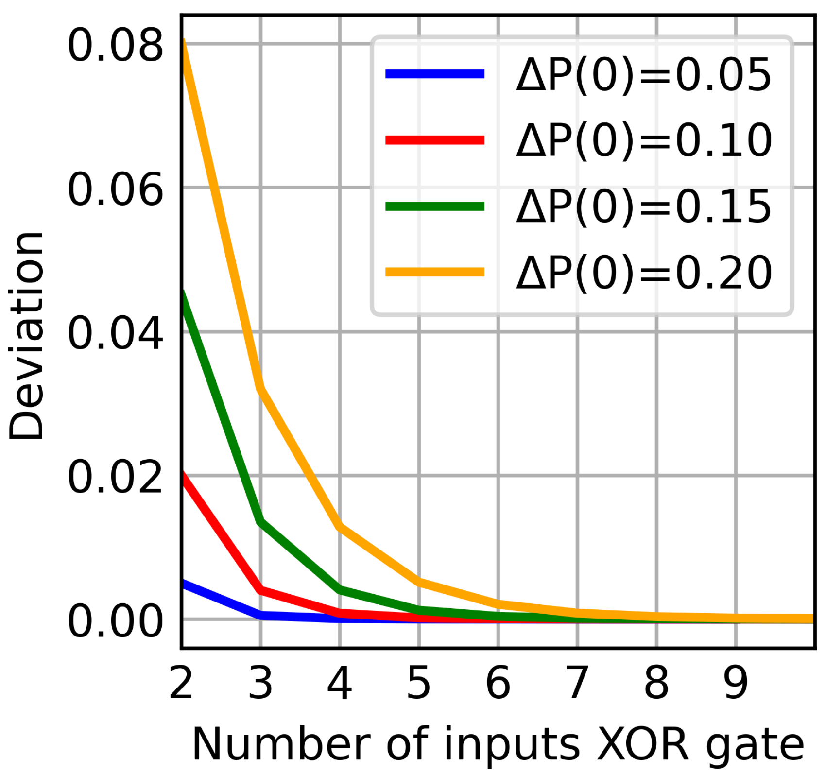
Figure 8 shows deviations for several values of
, where it can be noted that considering a maximum deviation in a SARO(1)-FF of
, minimum values of
N of 4 or 5 are required in order to obtain acceptable statistical results. It is also interesting to note that an increase of 5% in
implies a significant increase in the number of inputs of the XOR gate required for achieving the deviations below
. Indeed,
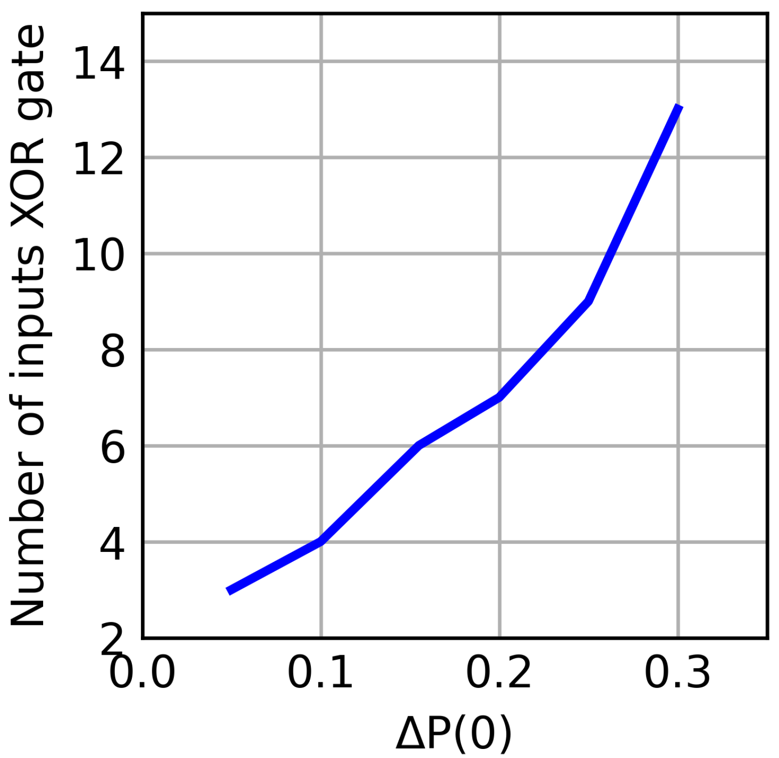
Figure 9 shows an exponential dependence of
N with
for maintaining a maximum deviation
. As
depends on the characteristic delay of LUTs, and this delay depends on the FPGA technology used, different types of FPGA can lead to quite different minimum
N values for passing NIST tests at a given sampling frequency. As an example, Spartan 6 (45nm technology) grade-3 devices from Xilinx report a delay of 0.21 ns from An-Dn LUT inputs to A-D outputs [
30], while Artix 7 (28 nm technology) grade-3 devices report a delay of 0.10 ns between the same points [
31]. This directly affects the time required for generating variability in these delays at a given sampling frequency, and consequently,
at this frequency.
In order to pass NIST tests for the Artix 7 device used in this work, if we introduce the experimental values obtained for
and introduce them in Equations (
4)–(
6), we can see that
implies a deviation of
at
= 50 KHz, which is in the limit of passing NIST frequency-based tests. In the case of
, we obtain
at
= 50 kHz, while theoretically, it should be around
.
Table 4 shows the NIST test results for this sampling frequency and parameters.
As has been presented, increasing the values of
N will improve frequency-based tests, but at the cost of an area increase. In order to achieve more compact implementations, we have explored decreasing
N and
k. To achieve an implementation passing NIST tests with
, the sampling frequency needs to be decreased.
Table 5 shows different implementations and sampling frequencies for MX-
N-SARO
. Note that it is possible to build a TRNG with
using SARO(1)-FF at a 33 kHz sampling frequency, and that
enables there to be TRNGs with a throughput of 100 Kbps (MX-4-SARO(1)) and a compact implementation requiring only four LUTs (MX-4-SARO(0)) in Artix 7 devices.
The area results regarding MX-4-SARO
from
Table 5 require a detailed explanation. Indeed, since a SARO(0)-FF includes a NAND gate, MX-4-SARO(0) is expected to require at least five LUTS: one LUT per two-input NAND gate and one LUT for the four-input XOR gate. Nevertheless, in seven-series devices from Xilinx, each six-input LUT has two independent outputs, named O5 and O6 [
32], thus being possible to implement the four SARO(0)-FFs in only two LUTs, as well as the four-input XOR in an additional LUT.
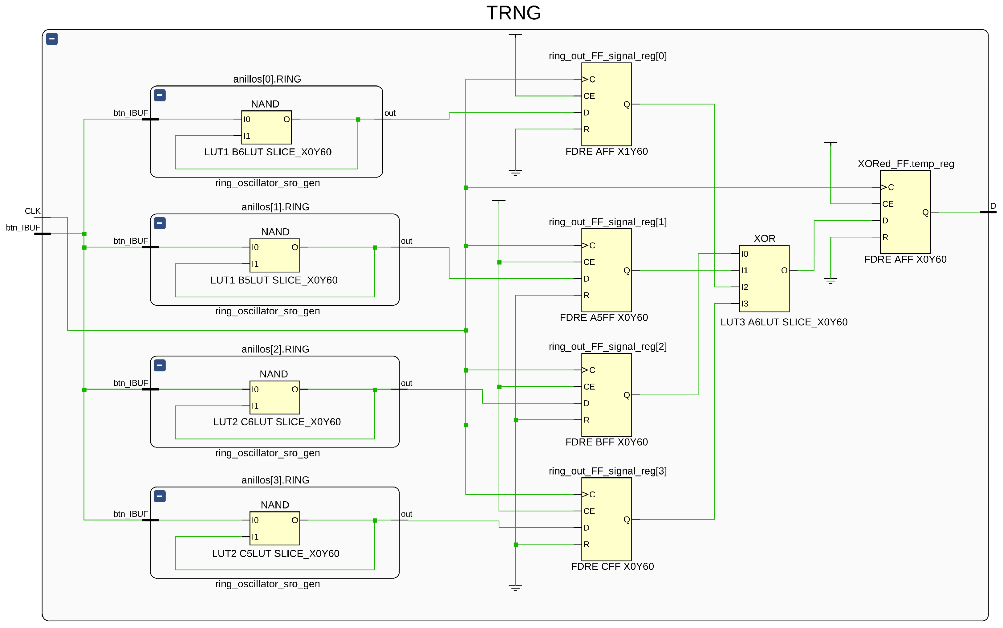
Figure 10 shows the mapping of MX-4-SARO(0) requiring three LUTs and five FFs. Similarly, MX-4-SARO(1) can be implemented using seven LUTs. Note that MX-3-SARO(1) fits in one slice, while MX-SARO(0) and MX-4-SARO(1) require two slices due to the five FFs to be placed.
From the results above, and taking into account Equations (
4) and (
6), it is possible to formulate a procedure to design and implement a TRNG based on the MX-
N-SARO
structure:
- 1.
Implement a SARO(1)-FF ring oscillator operating at the target sampling frequency corresponding to the desired throughput, following the scheme in
Figure 5.
- 2.
Capture a bitstream with a statistically significant size (), and analyze the frequency of ‘0’s and ‘1’s. The frequency test from the NIST suite can be used for this purpose. From this analysis, estimate the deviation probability of ‘0’s, .
- 3.
Use Equations (
4)–(
6) to estimate
N.
- 4.
Implement MX-
N-SARO
and perform NIST tests following the recommendations described in [
29] and summarized in
Section 3.
- 5.
In case NIST tests are not passed, increment N and go to 4.
This procedure enables compact TRNGs to be implemented on different FPGA technologies, optimizing the number of tries to achieve a low-cost design passing NIST tests.
5. Comparison to Other TRNGs for FPGAs
As commented in
Section 2, there are several proposals of TRNGs in the literature, mainly oriented to achieve high-throughput figures. In the case of systems with restrictions on area and/or performance, as is the case for Internet of Things (IoT) devices implemented on low-cost FPGAs, including cryptographic operations, the generation of 50 Kbps random streams is enough for the majority of applications. In this sense, our designs provide very compact TRNGs while ensuring randomness of the generated bitstreams.
Table 6 presents a comparison of MX-
N-SARO
to other compact implementations in the literature. In all cases, although they show contained area requirements, they are oriented to high-performance systems, where a large number of random numbers are required to be available continuously.
In this sense, the design in [
33] proposes the use of a set of multiple XORed ROs, followed by postprocessing based on a von Neumann corrector to improve entropy and statistical figures. As a result, it can achieve a throughput of 6 Mbps on a Spartan 3A device, from Xilinx Inc. at the cost of 528 LUT4s (Spartan 3A devices include 4-input LUTS). In the case of [
34], a different approach is used based on self-timed rings (STRs), and controlling dephases with the digital clock management (DCM) features included in Xilinx’s FPGAs. The results show a high throughput, 100 Mbps, with contained area requirements of 56 LUTs and 16 FFs on a Virtex 6 device, but in any case, this is far from the area figures presented in this work. Regarding [
35], this is also a high-throughput oriented TRNG, based on the use of DCMs to generate metastability, and bit-flipping postprocessing, which enables the improvement of throughput and area with respect to [
34], requiring around 38 LUTs on Zynq devices. The work in [
23] proposes two designs based on multiple XORed ROs, one with 25 ROs and the other one with 50 ROs, both implemented on Cyclone II devices from Intel. These designs can operate with a throughput of 100 Mbps, at the cost of more area requirements. In addition to the designs presented in
Table 6, the proposal in [
13] reports area requirements of four LUTs, similar to our proposal, but the required control logic is not included in those results, and it does not pass NIST tests in all cases [
35]. For these reasons, it has not been included in
Table 6. Regarding power consumption, the reduced number of ROs required by our proposal enables a contained power consumption of only 25 mW in the case of MX-3-SARO(1), and around 40 mW in the case of our designs with four ROs. These figures are clearly better than those carried out by the other works in
Table 6, except in the case of [
34]. Nevertheless, it should be noted that our results were obtained through a detailed analysis of the synthesized circuits using a N6705C DC Power Analyzer from Keysight, while the result in [
34] is an estimation provided by the ISE design tools from Xilinx. This estimation may be not reliable due to the difficulty that software tools have to estimate power consumption in feedback structures, as is the case of ROs.
6. Conclusions
In this work, the design of true random number generators for FPGAs based on multiple XORed ring oscillators has been revisited. Traditionally, in this type of design, a large quantity of parallel ring oscillators are used to achieve enough entropy and to pass the NIST SP 800-22 test suite, thus resulting in high area requirements. Our proposal shows that it is possible to pass NIST tests with a low number of ring oscillators when the sampling frequency is reduced, thus enabling the implementation of ultracompact TRNGs on low-cost FPGAs. Concretely, a design with three ring oscillators, requiring only three LUTs in Xilinx’s Artix 7 devices and providing a random bitstream at 33 Kbps, was implemented. With four ring oscillators of the MX-4-SARO(0) type, which also require three LUTs on Artix 7 devices, it is possible to achieve a throughput of 50 Kbps, while MX-4-SARO(1) achieves 100 Kbps, requiring only seven LUTs. Moreover, a procedure to migrate the designs to other FPGA technologies, optimizing the number of designs to test, was carried out. Finally, it should be noted that although the throughput presented by our designs is lower than other proposals in the literature, the area requirements are minimal, thus enabling their implementation on low-cost FPGAs for implementing secure IoT devices, including cryptographic algorithms.


 ,
, 


