
A Novel FPGA Implementation of the NAND-PUF with Minimal Resource Usage and High Reliability


Department of Information, Electronics and Communication Engineering (DIET), Sapienza University of Rome, 00184 Rome, Italy
*
Author to whom correspondence should be addressed.
Cryptography 2023, 7(2), 18; https://doi.org/10.3390/cryptography7020018
Submission received: 17 February 2023
/
Revised: 23 March 2023
/
Accepted: 30 March 2023
/
Published: 3 April 2023
(This article belongs to the Special Issue Feature Papers in Hardware Security II)
Abstract
:In this work we propose a novel implementation on recent Xilinx FPGA platforms of a PUF architecture based on the NAND SR-latch (referred to as NAND-PUF in the following) which achieves an extremely low resource usage with very good overall performance. More specifically, a 4 bit NAND-PUF macro has been designed referring to the Artix-7 platform occupying only 2 slices. The optimum excitation sequence has been determined by analysing the reliability versus the excitation time of the PUF cells under supply voltage variations. A 128 bit NAND-PUF has been tested on 16 FPGA boards under supply voltage and temperature variations and measured performances have been compared against state-of-the-art PUFs from the literature. The comparison has shown that the proposed PUF implementation exhibits the best reliability performance while occupying the minimum FPGA resource usage achieved in the PUF literature.
1. Introduction
Nowadays computer society has become more and more focused on the Hardware Security threat due to the increasing effectiveness of hardware attacks and tamper methods [1,2]. Indeed, though our smartphone, laptops and tablets are protected by secure software protocols, they are exposed to hardware attacks. The most common approach of modern cryptographic algorithms is to exploit secret keys stored in device’s memories to hide sensitive data. However, the great hypothesis of these security protocols is to assume that the cryptographic key stored on the device memory (which is used by the cryptographic algorithms) can’t be accessed by malicious attackers. Nowadays we can say that this is a too optimistic hypothesis since, in the last twenty years, researchers have investigated several tampering techniques such as micro-probing, focused ion beam, glitch attacks and side-channel attacks, demonstrating a fundamental weakness from the hardware security prospective in IoT devices [3,4,5,6,7]. Over the years researchers have focused on novel techniques to store secret keys in order to deal with hardware attacks and new tamper methods. Finally, the Physical Unclonable Functions (PUFs) have been introduced, demonstrating to be a secure mechanism to store cryptographic keys [8]. A PUF is a physical entity that produces an ideally unclonable output which depends on the physical implementation and characteristics of the device itself [9]. Indeed, PUFs are based on physical phenomena which exploit the peculiarity of the device’s silicon (given by mismatch and process variations), to extract a “fingerprint” that replaces the cryptographic key [10]. PUF-generated keys offer an advantage over traditional storage methods, like non-volatile memories (NVMs), as they are generated dynamically upon each usage, rather than being physically stored within the device [11]. Additionally, PUF-based devices can be challenging to reverse-engineer due to the unpredictable nature of manufacturing variations. This has led to the adoption of innovative security solutions utilizing PUFs, such as protection of intellectual property, anti-duplication/counterfeit prevention, and secure integrated circuit design [12,13,14,15,16]. Furthermore, PUFs allow also to reduce production costs by enabling mass-production with individualized security, providing a baseline solution for a hardware root-of-trust (RoT) [17]. PUFs can be designed both on application specific integrated circuits (ASICs) and Field Programmable Gate Arrays (FPGAs) by exploiting analog or digital approaches [11,18,19]. FPGAs are popular in both embedded and high-end systems due to their reconfigurable nature, performance, efficiency, and cost. However, hardware resources in FPGAs are limited, and integrating security modules can be difficult due to many constraints on the placement and routing of building blocks [20,21,22,23]. Therefore, the amount of entropy that can be extracted from a PUF cell placed on an FPGA is significantly impacted by the adopted placement and routing strategies [24].
The SRAM-based PUF uses the inherent variations in SRAM cells to generate a unique and unpredictable digital signature. It was introduced in [25,26], is based on the unpredictability of SRAM cells’ output at power up, and is one of the most popular PUFs. Even if SRAM-based PUFs have some advantages over traditional security methods, they have poor uniformity because the behavior of the SRAM cells can vary due to process, voltage, and temperature (PVT) variations, and also aging [27].
Ring-oscillator based PUFs (RO PUFs) [28,29,30] constitute another popular class of PUFs. RO PUFs generate the key by comparing the sampling frequency of two nominally identical ring oscillator chains. The difference in oscillation frequencies is due to mismatch variations in the delay chain. Due to the simple design, they are among the most used PUFs in FPGA implementations, resulting in very good reliability with respect to voltage and temperature variations. Despite the advantages, they exhibit also some challenges associated with the FPGA implementation. In fact, one of the main drawbacks of RO PUFs on FPGA platforms is the uniqueness, which results very low if compared with SRAM-based PUFs. In addition, this PUF architecture is affected by the locking phenomenon which dramatically reduces the reliability of the circuit. To mitigate this issue, Bousset et al. have proposed the Transient Effect Ring Oscillator PUF (TERO-PUF) [31], that is based on the oscillatory metastability of a TERO cell.
Arbiter PUFs and Interpose PUFs belong to another class of PUFs which has gained popularity due to the simple FPGA implementation [32]. These PUFs utilize differences in the delays of two or more delay lines caused by variations in the manufacturing process, resulting in unique identifiers. In [24] it has been proposed a compact version of the arbiter based PUF, suitable for FPGA implementation. The Pico PUF exploits an arbiter latch to select which of the two selected delay lines is faster [33].
Another important class of PUFs is the one of the metastable-based PUFs. Metastable-based PUFs exploit the metastability in cross coupled architectures to generate a unique key id relying on the peculiarity of silicon given by mismatch and process variations. One of the most renowned PUF is the Butterfly PUF [21]. The Butterfly PUF exploits the metastability of a pair of cross-coupled latches to generate an unique response. The simplicity of the architecture makes it suitable also for FPGA implementations. As further proposals of metastable cells the Differential Delay PUF (DD-PUF) [34,35] and the latched XOR-cell PUF [36] have been recently proposed in the literature. It has to be remarked that the latched XOR-cell PUF is a metastable-based PUF which exploits latched XOR elements to generate a transitory oscillation which results in a final stable state. From here on we refer to the PUF of [36] as meta-XOR-PUF. Both the DD-PUF and meta-XOR-PUF can be considered to implement a secure and robust PUF, as the delay differences are inherent to the manufacturing process and cannot be duplicated or precisely predicted [35]. Moreover, these PUFs are resistant to tampering methods, as any attempt to alter the IC will also alter the delay differences and result in a different response. However, with respect to the DD-PUF, the meta-XOR-PUF design requires lower resource consumption (just two XOR and AND gates) and thus offers benefits such as reduced cost and improved performance for applications where size and power consumption are critical.
The basic SR-Latch implemented by means of two cross-coupled NOR gates has been exploited to implement a PUF for the first time in [37], where a full-custom implementation referring to a 130 nm CMOS process is presented. Then in [38,39] two NAND-based SR-Latch PUFs have been proposed. More recently a revisited version of the NAND-based SR-Latch has been exploited to implement a PUF whose performances have been assessed through measurements on a single Altera Stratix III FPGA board in [40]. Another improved version of the NAND-based SR-Latch has been then presented in [41]. Both the PUF implementations in [40,41] and require additional gates to guarantee reliable operation of the NAND-PUF, resulting in relatively high FPGA resources usage.
In this work, we introduce a new implementation of the NAND-PUF which exploits a completely novel excitation strategy to guarantee high reliability while keeping the FPGA resources usage extremely low. The performances of the proposed implementation have been evaluated on several Xilinx Artix-7 (28 nm process) FPGA boards. The proposed PUF requires minimal resources usage (only two Look Up Tables) and demonstrates remarkable stability under voltage and temperature variations. To the best of our knowledge, this design is one of the most compact FPGA-compatible PUFs reported in the literature, offering 2 bits/slice density.
The organization of the paper is as follows: Section 2 outlines the PUFs metrics used to evaluate PUFs performance, in Section 3 the architecture of the NAND-PUF is analyzed and the FPGA implementation presented. Section 4 presents the results of the experimental validation, Section 5 compares the proposed NAND-PUF implementation with the state-of-the-art and finally in Section 6 conclusions are drawn.
2. Review of Main Performance Metrics for PUFs Evaluation and Comparison
Since PUFs are used in several authentication protocols such as, for example, the Challenge Response authentication, they have to be characterized through a rigorous analysis, and their performances have to be evaluated through standard metrics, which allow also to compare different PUF architectures. In the following we review the most commonly adopted metrics for PUFs performance evaluation: Uniformity, Randomness, Uniqueness, and Reliability.
Since PUFs should be exploited to generate a key, high entropy (e.g., Shannon entropy) has to be guaranteed in order to make the PUF-generated keys suitable for cryptographic purposes. Indeed, if the number of 0s of a PUF-generated key is exactly equal to the number of 1s, it means that the entropy of the key is 1 and no masking technique is required. The number of 0s and 1s is defined as Uniformity or also Bias of the response.
Though the Uniformity of a PUF gives information about the quality of the key of a given PUF implementation, it doesn’t give any information about the bistream 0 s and 1 s distribution. The Randomness of a PUF is a measure of the quality of the bitstream extracted in terms of statistical performances. Indeed, each PUF generates an n-bit response based on a specific challenge string. To guarantee the unpredictability of the key, Randomness must be assessed as specified in [42]. More specifically, according to [33,43,44,45,46], the Randomnes of a given PUF realization can be evaluated through a subset of NIST random tests [47]. Each test of the NIST suite produces a positive value p in the interval (p-value). The closer the p-value is to 1, the better the bitstream performs. The PUF bitstream passes the given test if the p-value is greater than 0.01 [35,43].
The Uniqueness of a PUF relies on its inherent randomness generated by the manufacturing variability of the underlying physical structure. The response of a PUF instance on silicon is unique to each device being given by a combination of mismatch and process variations associated to the manufacturing process of the integrated circuit. Therefore Uniqueness has to be quantified on different implementations of the same PUF circuit over different devices (FPGAs or chips). More specifically, the same design has to be physically implemented on different devices and each of these devices has to be excited with the same stimuli in the same environmental conditions. Then, the unique identifier (i.e., the collected response to a given challenge) has to be extracted from each device and the average value of the sum of inter-class Hamming Distance () between each possible pair-wise response couple has to be computed. According to [9], the inter-class HD is defined as:
where k are the realization of the PUF (i.e., the number of device under test), n are the bit of the response, () is the i-th response taken from the i-th implementation of the PUF. To ensure each PUF fingerprint is unpredictable, the same challenge applied to n PUFs should yield different responses. Therefore, the ideal n-chip inter-class Hamming Distance should be 50%.
The Reliability of a PUF is determined by how consistently it generates the same response to a given stimulus across different sessions and environmental conditions (i.e., different temperatures and different supply voltages). Indeed, some of the bit-cells of the PUF array could produce bits which vary when noise or voltage or temperature variations occur. These cells are called Unstable Cells and are related to the Reliability. It has to be noted that a given cell is considered unstable even if it generates just one output different from the others in a set of 1000 measurements. The Reliability is evaluated by selecting a reference challenge-response, and comparing it with new ones generated using the stimuli in different conditions. More specifically, the intra-class Hamming Distance () between the Golden-Key (GK) extracted in nominal condition, and k responses, collected in their respective power supply voltage and working temperature (typically of the nominal and T C,75 C]) is evaluated. In details, the Reliability is defined as follows [9]:
where represents the generated i-th response at a given power supply voltage and temperature, and the reference GK one. The evaluation of these metrics allows to characterize the PUF, covering a broad spectrum of possible working conditions.
Another widely adopted parameter to characterize a PUF is the Bit-Error-Rate (), defined as:
Since from the information of the BER in a given condition, the value of the Reliability can be extracted from Equation (2), the is often used in PUF evaluation instead of the Reliability. It has also to be remarked that each PUF is characterized by a nominal () due to transient noise variations which introduce noise in the excitation sequence of the PUF.
3. NAND-PUF Architecture and Design
The NAND-PUF architecture adopted in this work is depicted in Figure 1. It is composed by two NAND gates, denoted as and , arranged to implement a NAND SR-Latch circuit. The NAND-PUF exploits the prohibit excitation state (i.e., both the Set and Reset of the NAND latch equal to 0) of the SR-Latch to excite a fully symmetric circuit in order to generate an unique key response whose outcome ideally only depends on technology mismatch variations.
The main novelty of this paper is the excitation strategy adopted to increase the reliability of the basic SR-Latch. In order to gain insight into circuit behaviour and to better explain the proposed excitation sequence, the transistor level scheme depicted in Figure 2 can be utilized.
Referring to the value of the exitation signal , the excitation sequence can be splitted into two main intervals:
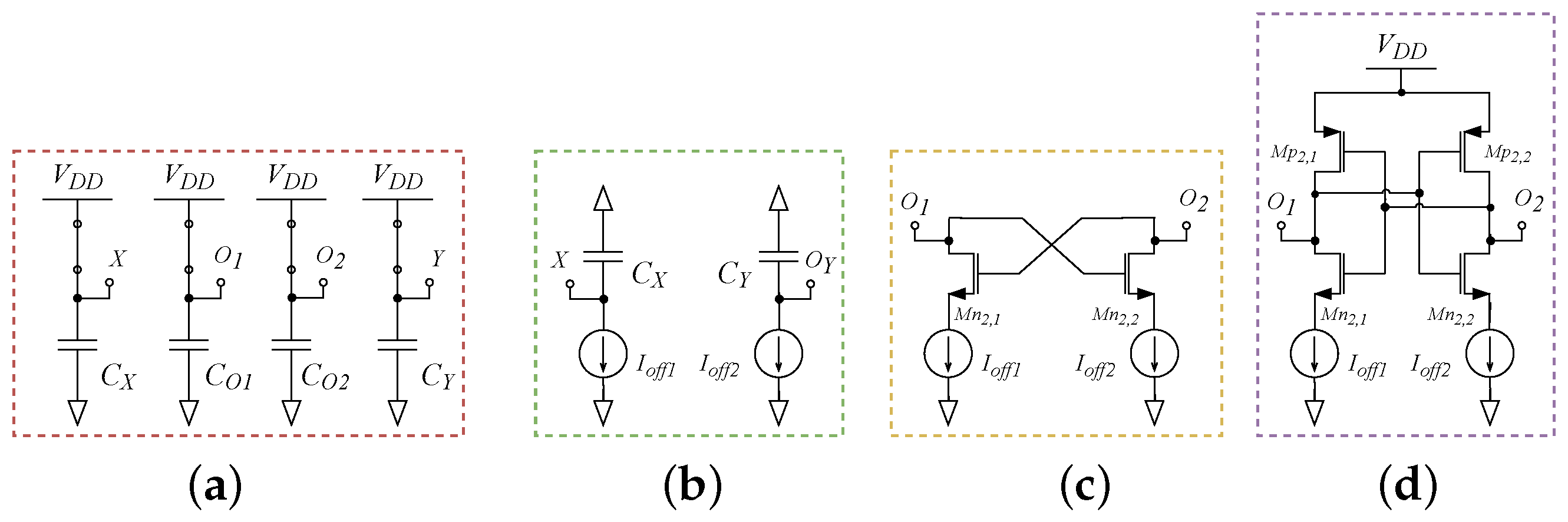
- When the signal is low (i.e., ), the outputs , X, Y and are set to and no current flows in and . More in detail, this excitation state forces the sources of and to , turning off transistors , , , and . The equivalent circuit in this phase is depicted in Figure 3a.
- When the signal is high (i.e., ), the operation of the circuit can be further divided into three different phases:
- (a)
- In the first phase, when Start goes high, transistors and are activated, while transistors , , , and are turned off. During this phase, the two transistors and discharge the parasitic capacitances at the source of and , which were previously charged to , until the gate-source voltage of and is greater than the threshold voltage . The equivalent circuit in this phase is depicted in Figure 3b.
- (b)
- In the second phase, the transistors and are in the saturation region with a and . The positive feedback between these transistors regenerates the current difference. In this phase and are turned off since their is equal to 0. The equivalent circuit in this phase is depicted in Figure 3c.
- (c)
- Finally, also the two transistors and are turned on and the positive feedback regenerates the signal until , producing a differential output voltage whose sign depends on the mismatch of the three transistors , , and , and the transistors , , and , respectively. The equivalent circuit in this phase is depicted in Figure 3d.
Thus, the working principle of the NAND-PUF relies on the conversion of a small current difference given by transistors and and guaranteed by mismatch variations, to generate a differential output voltage due to a positive feedback.
3.1. Architecture on FPGA
When referring to a semi-custom, standard-cell implementation of an ASIC, the NAND SR-Latch in Figure 1 can be easily implemented by using digital NAND gates taken from the standard-cell library of the technology. However this kind of straightforward implementation is not allowed on FPGA platforms, where the access to single digital gates is not available, and mux-based look-up tables are used to implement logic functions. Indeed, FPGAs are arranged as a matrix of Configurable Logic Blocks (CLBs). Each CLB contains programmable logic elements (such as lookup tables and flip-flops) and routing resources that can be configured by the user to implement custom digital logic circuits. CLBs are connected together to form the programmable interconnect fabric of the FPGA. They can be connected in various ways to create complex digital circuits, and the number and arrangement of CLBs in an FPGA determine its size and capacity. Each CLB contains two Slices which are complex blocks including the configurable digital blocks (synchronous and asynchronous) to implement digital operations. Each slice contains 8 Flip-Flops, 4 of which can be configured as Latches and 4 Look Up Tables (LUTs), each of which can be configured as a 6 inputs 1 output function or as a 5 input 2 outputs function. LUTs can be configured to perform the NAND function, thus for each NAND-PUF cell, just two LUTs are required. However, one of the most complex and at the same time critical step in the design of a PUF on FPGA is the symmetry of interconnections. If the interconnections are not balanced in terms of delay path, the response will be degraded, reducing the biasing performance and uniqueness of the PUF. To address this issue, manual balanced interconnections must be selected. In this work, a novel and original implementation of the NAND-PUF on an FPGA is presented, with accurate design to balance interconnection delays and NAND elements.
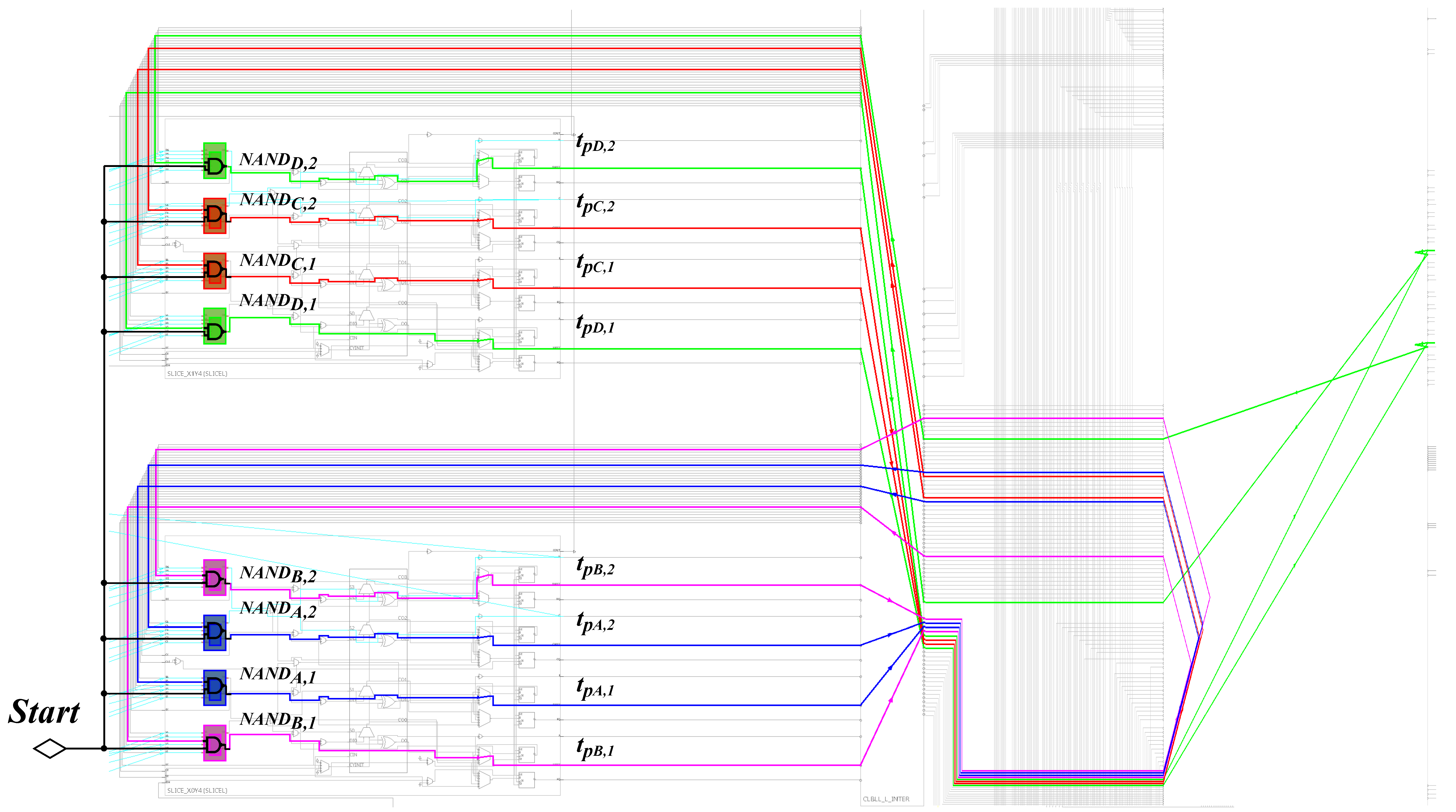
The macro of 4 NAND-PUF bit-cells implemented using 8 LUTs is shown in Figure 4. NAND gates and interconnections belonging to each of the 4 PUF cells have been highlighted with the same color, to visually show that the interconnections belonging to the same PUF bit exhibit a similar path lenght. To quantify paths delay in a more detailed way, a delay analysis on single paths and on the delay differences between pairwised paths has been carried out. The propagation delay of each of the 8 interconnections has been denoted as , where i assume values: and j assumes values: . Progation delay values obtained from the Xilinx Vivado design tool after place and route on the FPGA device are summarized in Table 1.
From that analysis it is clear that the difference in terms of propagation delay (denoted as ) is always lower than 20 ps, and thus nominally we can say that are well balanced, since mismatch variations would dominate over the systematic difference in the propagation delay. It should be emphasized that integrating the architecture on an FPGA introduces a routing delay which alters the behavior of the NAND PUF. As a result, a phenomenon similar to the one described in [48,49,50] is observed. Nevertheless, as shown in [34], the delay difference caused by mismatches still determines the output value (either 0 or 1).
3.2. Comparison with Respect to Previous SR-NAND Latch Implementations
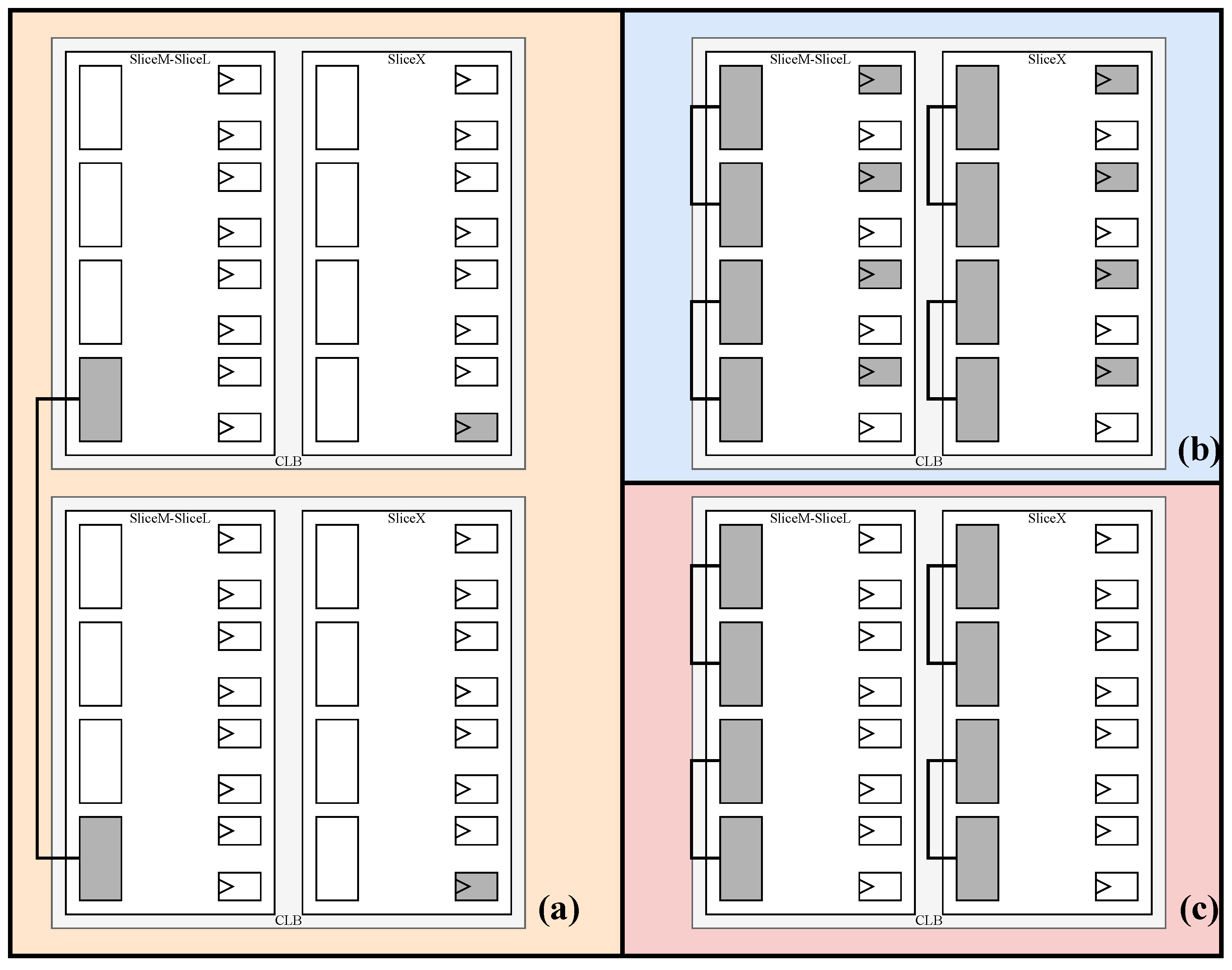
The literature already contains various implementations of NAND-based SR-latches, such as those presented in [38,39]. In [38], a new method for utilizing unstable bits from SR-latches was proposed. By exploiting the position of these unstable bits, the variety of responses was increased from to an ideal value of . However, the FPGA implementation of the PUF presented here differs from the one in [38]. In the implementation on the Spartan-3e of [38], the focus was on guaranteeing a maximum of 43 unstable cells to maximize the possible challenge-response pair set. To achieve this, a flip-flop was added before the NAND latch, increasing the number of unstable bits in the response and reducing the skew between the two NAND gates. This design implementation required two LUTs and one flip-flop, and was integrated into a single CLB on the Spartan-3E. The authors of [38] also presented an implementation on the Spartan-6 in which two NAND cells and two flip-flops were used to reproduce the same architecture as in [51]. This implementation has an high impact on the hardware resources, requiring four different Slices for each instance.
Another NAND based SR-latch was designed on a Spartan-6 in [39]. The architecture of [39] was integrated with a resource consumption of half slice, very similar to [33,34,35,36,52]. Such implementation has been already reported in [38,51]. However, authors inserted an explicit reset condition in [39] through two Flip-Flops positioned in front of the latch. It has to be remarked that, even if the implementation on FPGA of [38,39] are similar to the one presented in this work, the key extraction relies on different sources of entropy. Indeed, in [38] authors extracts the key directly from the final state of the NAND latch, however selecting the most reliable 128 PUF-cells among the 512 instantiated, whereas in [39] the information comes by the number of oscillations that each SR latch made until it finds the steady state.
The proposed design exhibits several differences with respect to previous approaches: first of all, we exploits only the SR NAND latch, and through the custom routing strategy we guarantee a good matching between the two delay paths, providing good uniqueness and ensuring the metastability of the SR latch without the exploitation of two additional flip-flops. In terms of hardware resources, we implement 4 instances in a single CLB, and each instance exploits just two LUTs. Thus, the 4 LUTs of each Slice are occupied by the 4 NAND cells. Furthermore, we implement the 128 bit macro with considering 32 CLB, arranged in a 8 × 4 matrix. In Figure 5 the FPGA implementation of [38,39] and this work have been depicted. The enabled LUTs and Flip-Flops of CLBs have been highlighted in gray color.
4. Experimental Results
In this section, we report experimental results on the evaluation of the proposed NAND-PUF. As a case study, we have considered a 128-bit NAND-PUF cell array, meaning that 32 4-bit macros have been placed in a 8 × 4 array. Adopting a macro-based design allowed us to preserve the balanced internal routing and structure of the NAND-PUF cells. The analysis of the proposed implementation has been carried out by considering a broad range of experimental aspects, in order to fully cover its behavior with PVT variations.
4.1. Testbed of the NAND-PUF
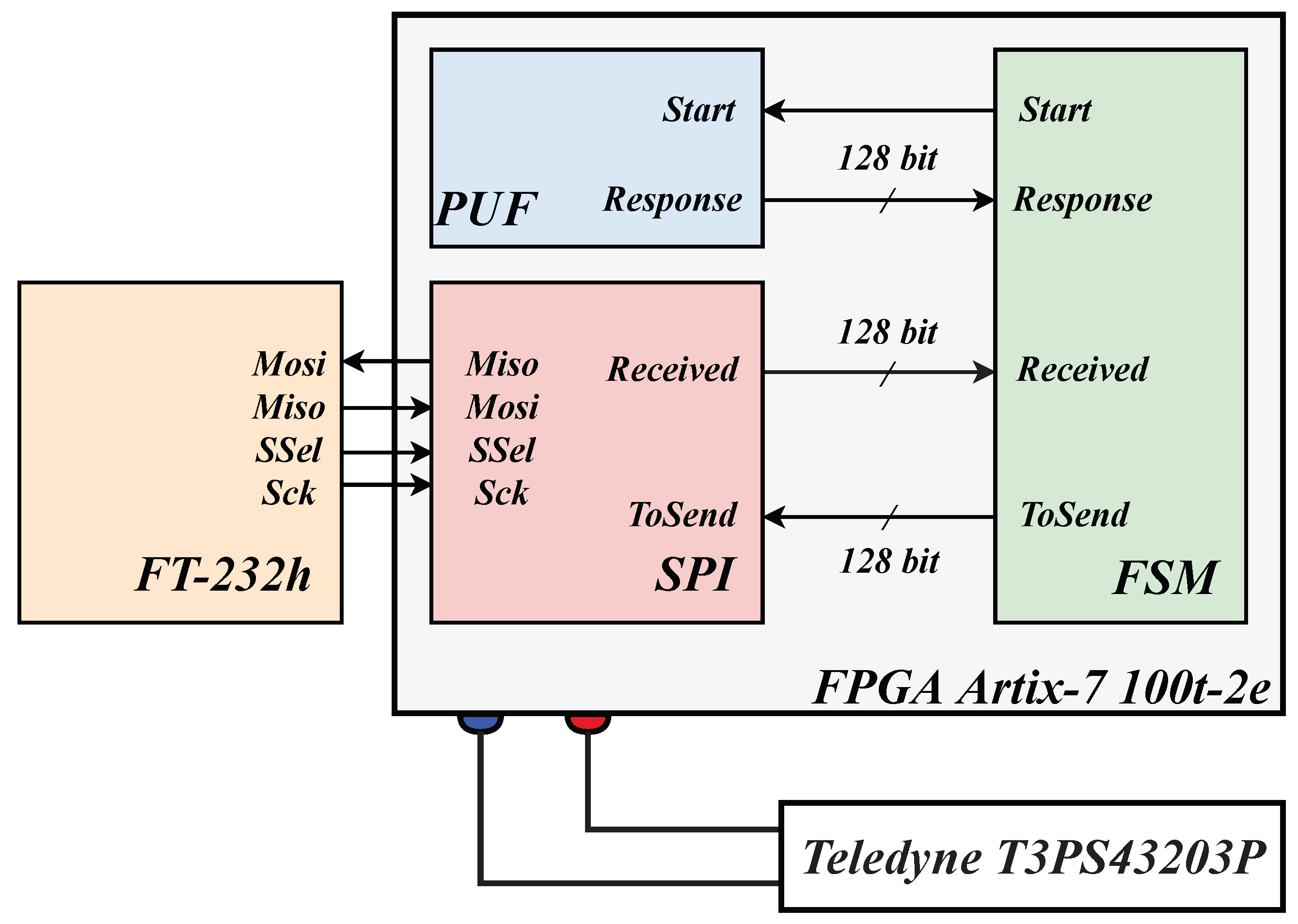
Our evaluation campaign has involved 16 boards, mounting Xilinx Artix-7 100t FPGAs. FPGAs’ core voltage has been supplied by means of Teledyne T3PS43203P programmable power supply unit. We have considered a supply voltage range of around the nominal one, which is 0.9V (model-2e of the Xilinx Artix-7). The working temperature of the FPGA has been accurately set by using an Espec SH-621 climate chamber, in the range [5C,80 C]. A system clock of 50 MHz has been used for all the measurements. We refer hereon to the duration of the Start signal as in number of clock cycles, considering the system clock period as timing reference.
All boards are supervised through a daughter board mounting a FT232H chip, which serves as USB-SPI interface, stimulated by custom Python scripts. The duration of the Start signal can be changed through the SPI. By means of this simple but effective testbed, we have been able to evaluate the steadyness of the proposed PUF under different stimuli conditions, revealing some interesting features when power supply voltage variations take hold. The block scheme of the adopted testbed is depicted in Figure 6.
4.2. Reliability, Bias, Unstable Cells and Uniqueness
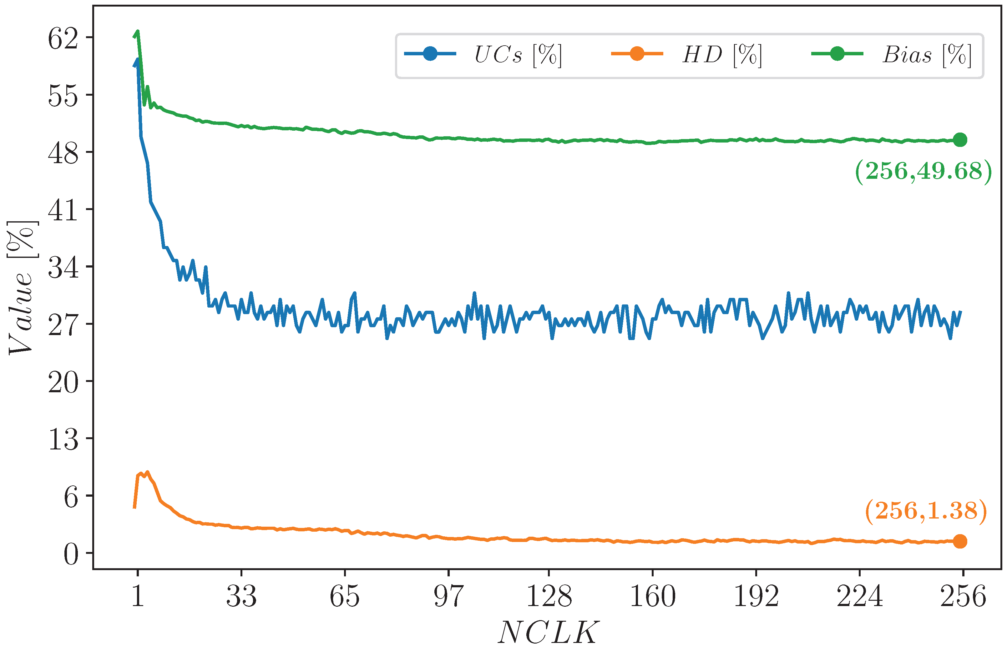
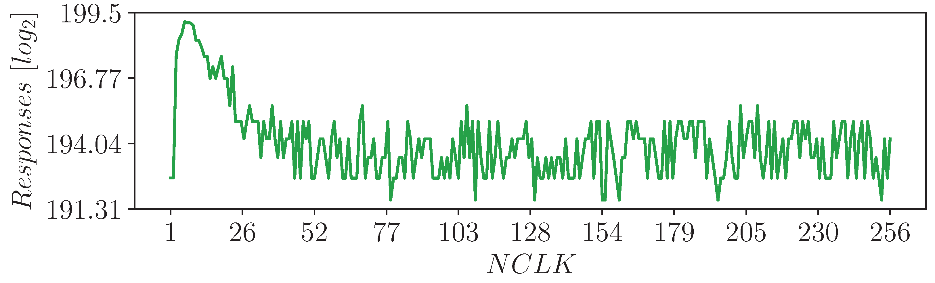
In order to evaluate the performance of the proposed NAND-PUF and evaluate the impact of the start stimuli over main performance parameters, we have measured responses for different time-durations () of the signal ranging from 1 up to 256 clock cycles. The BER in terms of Intra Hamming Distance in orange, the Bias of the response in green and the Unstable Cells (UCs) in blue are reported in Figure 7 as a function of . As it can be observed, the time in which the output is sampled has an impact on both the UCs and the BER. The more time the PUF array cells are leaved to run, the lower the number of UCs will be, and, as a consequence, a lower BER and a higher Reliability will be achieved.
It has to be pointed out, however, that in this reasoning, we are losing a key parameter, which is the BER when supply voltage variations occur. In order to consider also this point in our discussion, we tested for 30 different values of the reliability of the PUF when the voltage varies of and results of the measurement campaign over a reference board (the one also used for the analysis of Figure 7) are reported in Figure 8 as an heatmap whose values are written in each box.
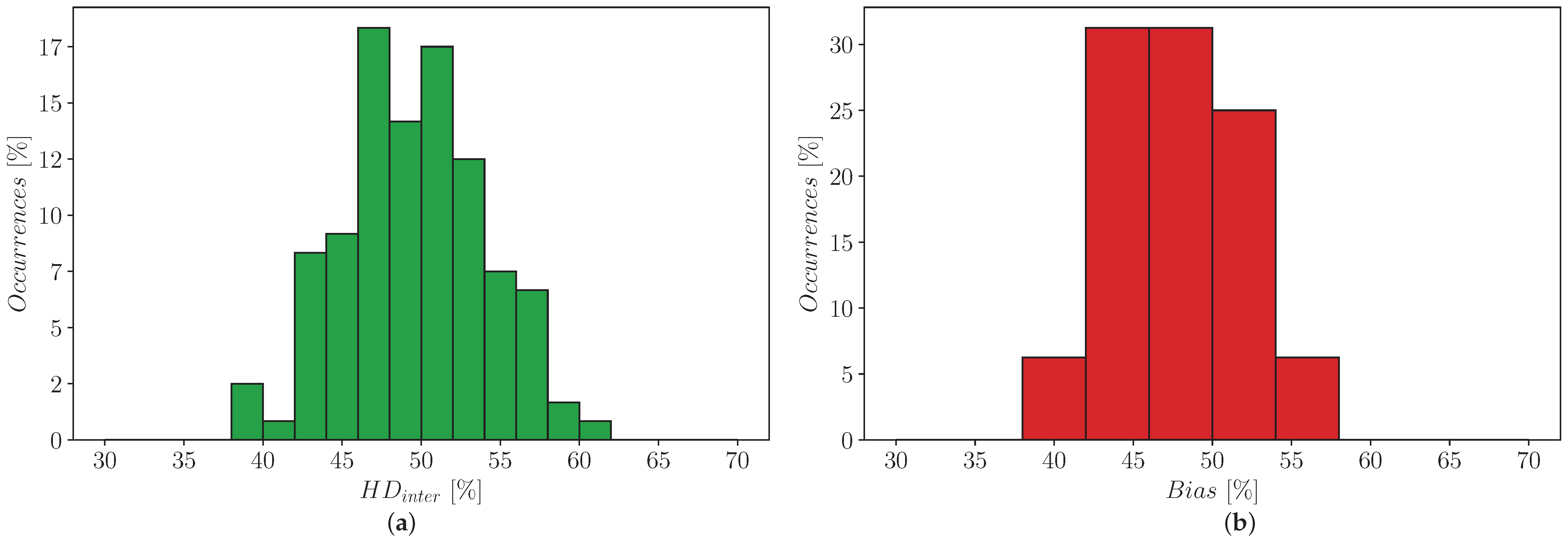
The inter-class HD over 16 Artix-7 boards is depicted in Figure 9, with the values on the x-axis reported as a percentage of 128-bit responses. The mean value of the inter-class HD has been found to be 49.50% with a standard deviation of 4.59%. As can be seen, the obtained values are very close to the ideal value of 50%, confirming the effectiveness of the proposed implementation and in particular of the routing strategy. Indeed, these results demonstrate that the proposed NAND-PUF implementation is able to efficiently extract entropy from the manufacturing process and our statistical analysis of responses from different devices implementing the same circuit did not reveal any structured artifacts (unbalanced routing or significant unbiased cells).
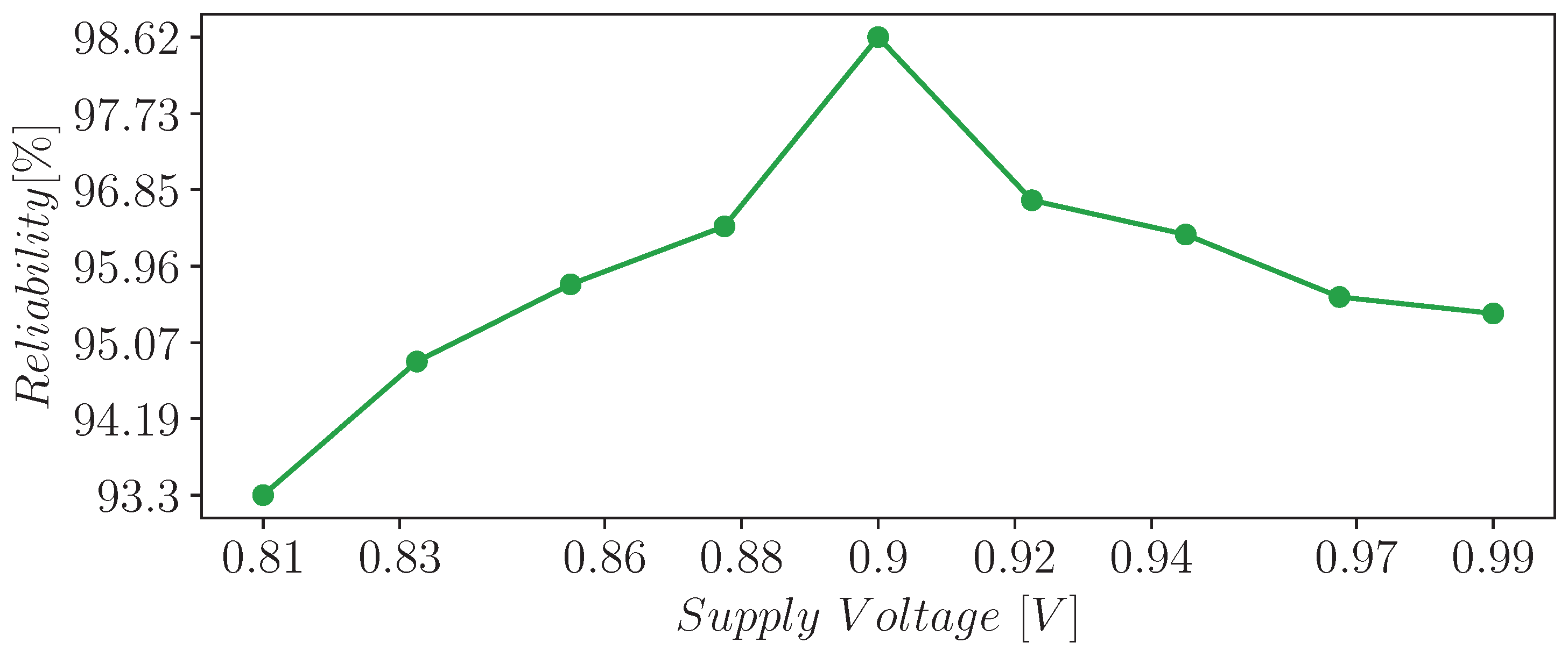
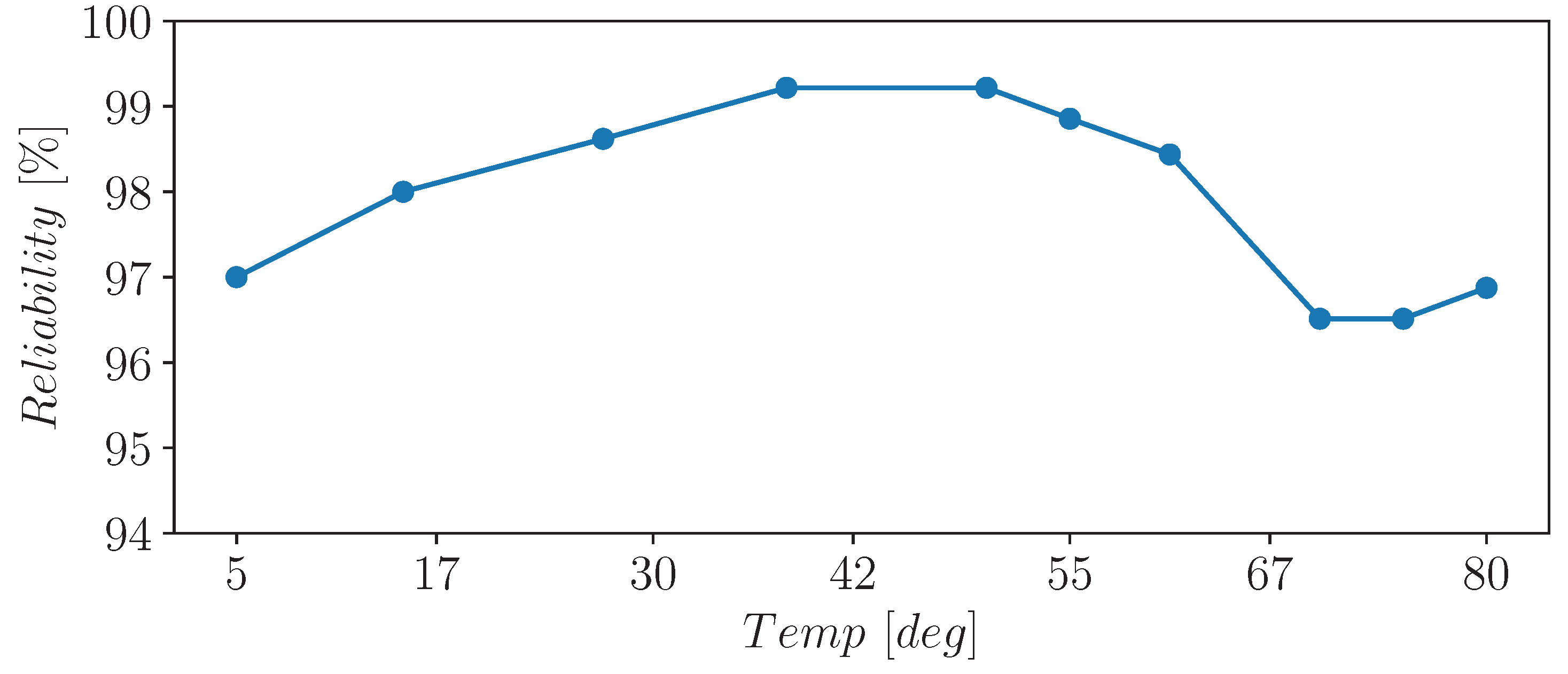
In typical condition (i.e., V) the is always good (see Figure 7) but under supply voltage variations the number of unstable cells for low values of increases and the Reliability worsens. However, for greater than 128 the Reliability is good also at the two supply voltage corners. According to this analysis we have chosen to implement an excitation sequence which guarantees high performance even under supply voltage variations. Once selected the number of clock cycles on which the Start signal has to be set high, we tested reliability performance of the NAND-PUF with respect to voltage and temperature variations. Experimental results are reported in Figure 10 and Figure 11. As it can be observed, in both the tests, the Reliability is always greater than 93% and, it is evident that the impact of voltage variations is stronger than the one of temperature variations. Indeed, the worst case corner for temperature variation is met at approximately 70 C, which is about 96%, that can be considered good also with respect to nominal corner, indeed it is worsened of about 2%, which is a very good result considering that the architecture is implemented on an FPGA and not on an ASIC.
4.3. Enhancing the Set of Possible Responses
In [38] a technique to enhance the set of responses by exploiting unstable cells positions has been proposed. Denoting with the number of unstable cells, the set of possible responses can be expanded to:
where denotes the number of combinations of 128 elements taken UC at a time as in [38]. The upper bound of this technique is given when 128/3 unstable cells are generated. We investigated the performance of this technique when is changed and experimental results have been depicted in Figure 12. These results are extracted from 1000 repeated read-out responses from each location, in accordance with [38].
As it can be observed, the best number of unstable cells is reached at .
4.4. Randomness and Uniformity Results
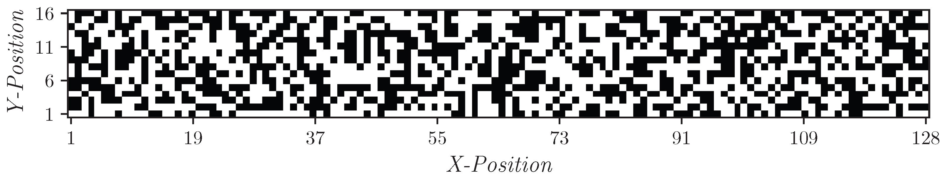
In this section, experimental results of a thorough measurement campaign over 16 FPGA boards is reprted, with the aim of evaluating the Randomness of the proposed NAND-PUF implementation. NIST tests have been carried out according to [53,54]. The results of these tests are presented in Table 2. In Figure 13 a visual representation of the 128 × 16 bits extracted from the 16 devices is depicted and from that figure, by a visual inspection it is clear that the generated sequences are uncorrelated. We found that produced responses over 16 boards met the minimum requirements to pass all tests. We further calculated the average bias of the response by taking the mean of the 16 devices’ responses. Results have shown that the bias of the NAND-PUF is approximately 46.85% with a standard deviation of 4.06%. Experiments revealed that the best uniformity was achieved in 3 of the 16 tested devices, with 1/0 bias values of 50.00%. These results suggest that the proposed NAND-PUF design effectively exploits process and mismatch variations, and there is no evidence of systematic bias. It can therefore be concluded that with a larger number of devices, the bias would converge to a mean value closer to the ideal one of 50%. It’s important to note that the responses used in this analysis were taken without any post-processing or elaboration techniques.
5. Comparison with State-of-the-Art
In order to compare performances of different PUF designs we introduce the following figures of merit (FOMs):
and their version normalized with respect to the resource consumption:
where is the measured in typical conditions by multiple repeated measurements (), and denote the maximum range of voltage and temperature variations assumed in the measurements respectively, and is the worst case measured under voltage and temperature variations respectively. Finally the is the number of PUF-bits which can be implemented in a single FPGA Slice.
According to the above definitions, and evaluate both how good the Reliability and Uniqueness of a given PUF are, whereas takes into account also the resource consumption in terms of bits/Slice. The higher the and are, the better the PUF performs with respect to Uniqueness and Reliability. The evaluates how good is the Reliability with respect to Voltage (), Temperature () and Transient Noise () variations in selected variation ranges (r.g. ) for a given PUF implementation. The takes into account also the resource consumption. The lower is the , the higher the is. Thus an higher implies a lower impact on PUF-generated key when environmental variations come.
The proposed NAND-PUF implementation has then been compared with other FPGA-integrated PUF architectures and main metrics are summarized in Table 3. For what concerns the Uniqueness and the Reliability in nominal conditions, the proposed PUF results comparable with the state-of-the-art.
By considering the required resources in terms of Slices and CLBs, the proposed design is comparable to [34,36] and is among the most compact architectures deployed on FPGA. However, PUF-primitives employed in [24,33,34,52] occupies two LUTs and two flip-flops while the here proposed design demands just two LUTs, thus outperforming the above mentioned implementations. Indeed, with respect to the which evaluates also the resource consumption, it is clear that [36] outperforms other works, but it is followed by the proposed work in terms of performance.
On the other hand, among the most compact architecture on FPGA (i.e., the ones which occupy 0.5 Slice/bit), the proposed architecture has resulted to be the most reliable one, reaching the best . If compared with works which employ more hardware resources, it is overcome by just [39] which however has 4 times the resource consumption and requires also some post-processing to select the most reliable cells among the ones instantiated on FPGA.
6. Conclusions
In this work the NAND-PUF architecture has been successfully implemented on Xilinx FPGAs for the first time, with a focus on the Artix-7 platform achieving a resouce usage as low as 0.5 slices per bit. The macro of 4 NAND-PUF bit-cells implemented using 2 slices has been optimized with custom place and route scripts to achieve delay balancing with differences in terms of propagation delay lower than 20 ps, thus guaranteeing that mismatch variations would dominate over the systematic difference in the propagation delay. The reliability of the proposed implementation has been strongly improved with respect to previous works dealing with SR-Latch-based PUFs by using a novel excitation approach. The optimum excitation sequence has been determined through a thorough measurement campaign considering supply voltage variations. A 128-bit PUF cell array, implemented as 32 balanced 4-bit macros has been tested on 16 Artix 7 FPGA boards, and the results have been compared to state-of-the-art PUFs. The comparison has demonstrated that the proposed implementation exhibits comparable performance with state-of-the-art PUFs in terms of Uniqueness and Reliability in nominal conditions, while occupying the minimum FPGA resource count achieved in the literature. In addition, the proposed NAND-PUF reaches the best trade-off with respect to resource consumption and Reliability, reaching the best of about 5.961, generating 2 bits/Slice.
Author Contributions
Conceptualization, R.D.S.; methodology, R.D.S. and G.S.; software, R.D.S.; validation, R.D.S.; formal analysis, R.D.S.; investigation, R.D.S. and G.S.; resources, G.S.; data curation, R.D.S.; writing—original draft preparation, R.D.S.; writing—review and editing, G.S.; visualization, G.S.; supervision, G.S.; project administration, G.S. All authors have read and agreed to the published version of the manuscript.
Funding
This research received no external funding.
Data Availability Statement
Not applicable.
Conflicts of Interest
The authors declare no conflict of interest.
References
- Desai, A.R.; Hsiao, M.S.; Wang, C.; Nazhandali, L.; Hall, S. Interlocking obfuscation for anti-tamper hardware. In Proceedings of the Eighth Annual Cyber Security and Information Intelligence Research Workshop (CSIIRW’13), Oak Ridge, TN, USA, 8–10 January 2013; Association for Computing Machinery: New York, NY, USA, 2013; pp. 1–4. [Google Scholar]
- Ravi, S.; Raghunathan, A.; Chakradhar, S. Tamper resistance mechanisms for secure embedded systems. In Proceedings of the 17th International Conference on VLSI Design, Mumbai, India, 9 January 2004; pp. 605–611. [Google Scholar]
- Biham, E.; Shamir, A. Differential fault analysis of secret key cryptosystems. In Advances in Cryptology— CRYPTO ’97; Springer: Berlin, Germany, 2006; pp. 513–525. [Google Scholar]
- Wang, H.; Forte, D.; Tehranipoor, M.M.; Shi, Q. Probing Attacks on Integrated Circuits: Challenges and Research Opportunities. IEEE Des. Test 2017, 34, 63–71. [Google Scholar] [CrossRef]
- Randolph, M.; Diehl, W. Power Side-Channel Attack Analysis: A Review of 20 Years of Study for the Layman. Cryptography 2020, 4, 15. [Google Scholar] [CrossRef]
- Zhou, Y.; Feng, D. Side-Channel Attacks: Ten Years After Its Publication and the Impacts on Cryptographic Module Security Testing. Cryptol. ePrint Arch. 2005. Available online: https://eprint.iacr.org/2005/388 (accessed on 16 February 2023).
- Koeune, F.; Standaert, F.X. A Tutorial on Physical Security and Side-Channel Attacks. In Foundations of Security Analysis and Design III: FOSAD 2004/2005 Tutorial Lectures; Springer: Berlin, Germany, 2005; pp. 78–108. [Google Scholar]
- Rührmair, U.; Holcomb, D.E. PUFs at a glance. In Proceedings of the 2014 Design, Automation Test in Europe Conference Exhibition (DATE), Dresden, Germany, 24–28 March 2014; pp. 1–6. [Google Scholar] [CrossRef]
- Böhm, C.; Hofer, M. Physical Unclonable Functions in Theory and Practice; Springer: Berlin/Heidelberg, Germany, 2012. [Google Scholar]
- Halak, B. Physically Unclonable Functions: From Basic Design Principles to Advanced Hardware Security Applications; Springer: Berlin/Heidelberg, Germany, 2018. [Google Scholar]
- Shamsoshoara, A.; Korenda, A.; Afghah, F.; Zeadally, S. A survey on physical unclonable function (PUF)-based security solutions for Internet of Things. Comput. Netw. 2020, 183, 107593. [Google Scholar] [CrossRef]
- Qureshi, M.A.; Munir, A. PUF-RAKE: A PUF-based Robust and Lightweight Authentication and Key Establishment Protocol. IEEE Trans. Dependable Secur. Comput. 2021, 19, 2457–2475. [Google Scholar] [CrossRef]
- Johnson, A.P.; Chakraborty, R.S.; Mukhopadhyay, D. A PUF-enabled secure architecture for FPGA-based IoT applications. IEEE Trans. Multi-Scale Comput. Syst. 2015, 1, 110–122. [Google Scholar] [CrossRef]
- Chatterjee, U.; Govindan, V.; Sadhukhan, R.; Mukhopadhyay, D.; Chakraborty, R.S.; Mahata, D.; Prabhu, M.M. Building PUF based authentication and key exchange protocol for IoT without explicit CRPs in verifier database. IEEE Trans. Dependable Secur. Comput. 2018, 16, 424–437. [Google Scholar] [CrossRef]
- Suh, G.E.; Devadas, S. Physical Unclonable Functions for Device Authentication and Secret Key Generation. In Proceedings of the 2007 44th ACM/IEEE Design Automation Conference, San Diego, CA, USA, 4–8 June 2007; pp. 9–14. [Google Scholar]
- Yilmaz, Y.; Gunn, S.R.; Halak, B. Lightweight PUF-based authentication protocol for IoT devices. In Proceedings of the 2018 IEEE 3rd International Verification and Security Workshop (IVSW), Costa Brava, Spain, 2–4 June 2018; pp. 38–43. [Google Scholar]
- Zhao, S.; Zhang, Q.; Hu, G.; Qin, Y.; Feng, D. Providing Root of Trust for ARM TrustZone using On-Chip SRAM. In Proceedings of the 4th International Workshop on Trustworthy Embedded Devices, (TrustED ’14), Scottsdale, AZ, USA, 3 November 2014; Association for Computing Machinery: New York, NY, USA, 2014; pp. 25–36. [Google Scholar]
- Della Sala, R.; Bellizia, D.; Centurelli, F.; Scotti, G. A Monostable Physically Unclonable Function Based on Improved RCCMs with 0–1.56% Native Bit Instability at 0.6–1.2 V and 0–75 °C. Electronics 2023, 12, 755. [Google Scholar] [CrossRef]
- Zerrouki, F.; Ouchani, S.; Bouarfa, H. A survey on silicon PUFs. J. Syst. Archit. 2023, 127, 102514. [Google Scholar] [CrossRef]
- Majzoobi, M.; Koushanfar, F.; Devadas, S. FPGA PUF using programmable delay lines. In Proceedings of the 2010 IEEE International Workshop on Information Forensics and Security, Seattle, WA, USA, 12–15 December 2010; pp. 1–6. [Google Scholar]
- Kumar, S.S.; Guajardo, J.; Maes, R.; Schrijen, G.J.; Tuyls, P. The Butterfly PUF: Protecting IP on every FPGA. In Proceedings of the IEEE International Workshop on Hardware-Oriented Security and Trust, HOST 2008, Anaheim, CA, USA, 9 June 2008; pp. 67–70. [Google Scholar]
- Anderson, J.H. A PUF design for secure FPGA-based embedded systems. In Proceedings of the 2010 15th Asia and South Pacific Design Automation Conference (ASP-DAC), Taipei, Taiwan, 18–21 January 2010; pp. 18–21. [Google Scholar]
- Maiti, A.; Schaumont, P. Improved Ring Oscillator PUF: An FPGA-friendly Secure Primitive. J. Cryptol. 2011, 24, 375–397. [Google Scholar] [CrossRef]
- Gu, C.; Chang, C.H.; Liu, W.; Hanley, N.; Miskelly, J.; O’Neill, M. A large-scale comprehensive evaluation of single-slice ring oscillator and PicoPUF bit cells on 28-nm Xilinx FPGAs. J. Cryptogr. Eng. 2021, 11, 227–238. [Google Scholar] [CrossRef]
- Guajardo, J.; Kumar, S.S.; Schrijen, G.J.; Tuyls, P. FPGA Intrinsic PUFs and Their Use for IP Protection. In International Workshop on Cryptographic Hardware and Embedded Systems; Paillier, P., Verbauwhede, I., Eds.; Lecture Notes in Computer Science; Springer: Berlin/Heidelberg, Germany, 2007; Volume 4727, pp. 63–80. [Google Scholar]
- Holcomb, D.E.; Burleson, W.P.; Fu, K. Power-Up SRAM State as an Identifying Fingerprint and Source of True Random Numbers. IEEE Trans. Comput. 2008, 58, 1198–1210. [Google Scholar] [CrossRef]
- Garg, A.; Kim, T.T. Design of SRAM PUF with improved uniformity and reliability utilizing device aging effect. In Proceedings of the 2014 IEEE International Symposium on Circuits and Systems (ISCAS), Melbourne, VIC, Australia, 1–5 June 2014; pp. 1941–1944. [Google Scholar]
- Gao, M.; Lai, K.; Qu, G. A Highly Flexible Ring Oscillator PUF. In Proceedings of the 51st Annual Design Automation Conference (DAC’14:), San Francisco, CA, USA, 1–5 June 2014; Association for Computing Machinery: New York, NY, USA, 2014; pp. 1–6. [Google Scholar]
- Yin, C.E.; Qu, G. Temperature-aware cooperative ring oscillator PUF. In Proceedings of the 2009 IEEE International Workshop on Hardware-Oriented Security and Trust, San Francisco, CA, USA, 27 July 2009; p. 27. [Google Scholar]
- Xin, X.; Kaps, J.P.; Gaj, K. A Configurable Ring-Oscillator-Based PUF for Xilinx FPGAs. In Proceedings of the 2011 14th Euromicro Conference on Digital System Design, Oulu, Finland, 31 August–2 September 2011; pp. 651–657. [Google Scholar]
- Bossuet, L.; Ngo, X.T.; Cherif, Z.; Fischer, V. A PUF Based on a Transient Effect Ring Oscillator and Insensitive to Locking Phenomenon. IEEE Trans. Emerg. Top. Comput. 2014, 2, 30–36. [Google Scholar] [CrossRef]
- Lim, D.; Lee, J.W.; Gassend, B.; Suh, G.E.; van Dijk, M.; Devadas, S. Extracting secret keys from integrated circuits. IEEE Trans. Very Large Scale Integr. (VLSI) Syst. 2005, 13, 1200–1205. [Google Scholar] [CrossRef]
- Gu, C.; O’Neill, M. Ultra-compact and robust FPGA-based PUF identification generator. In Proceedings of the 2015 IEEE International Symposium on Circuits and Systems (ISCAS), Lisbon, Portugal, 24–27 May 2015; pp. 934–937. [Google Scholar]
- Della Sala, R.; Bellizia, D.; Scotti, G. A Novel Ultra-Compact FPGA PUF: The DD-PUF. Cryptography 2021, 5, 23. [Google Scholar] [CrossRef]
- Della Sala, R.; Scotti, G. The DD-Cell: A Double Side Entropic Source exploitable as PUF and TRNG. In Proceedings of the 2022 17th Conference on Ph.D. Research in Microelectronics and Electronics (PRIME), Villasimius, SU, Italy, 12–15 June 2022; pp. 353–356. [Google Scholar]
- Della Sala, R.; Bellizia, D.; Scotti, G. A Lightweight FPGA Compatible Weak-PUF Primitive Based on XOR Gates. IEEE Trans. Circuits Syst. II Express Briefs 2022, 69, 2972–2976. [Google Scholar] [CrossRef]
- Su, Y.; Holleman, J.; Otis, B. A 1.6pJ/bit 96% Stable Chip-ID Generating Circuit using Process Variations. In Proceedings of the 2007 IEEE International Solid-State Circuits Conference. Digest of Technical Papers. San Francisco, CA, USA, 11–15 February 2007; pp. 406–611. [Google Scholar] [CrossRef]
- Yamamoto, D.; Sakiyama, K.; Iwamoto, M.; Ohta, K.; Takenaka, M.; Itoh, K. Variety enhancement of PUF responses using the locations of random outputting RS latches. J. Cryptogr. Eng. 2013, 3, 197–211. [Google Scholar] [CrossRef] [Green Version]
- Habib, B.; Kaps, J.P.; Gaj, K. Efficient SR-Latch PUF. In Applied Reconfigurable Computing; Springer: Cham, Switzerland, 2015; pp. 205–216. [Google Scholar]
- Bai, Y.; Wu, L.; Wu, X.; Li, X.; Zhang, X.; Wang, B. PUF-based encryption method for IC cards on-chip memories. Electron. Lett. 2016, 52, 1671–1673. [Google Scholar] [CrossRef]
- Khuchit, U.; Bai, Y.; Wu, L.; Zhang, X. An Improved Cross-Coupled NAND Gates PUF for Bank IC Card. In Proceedings of the 2nd International Conference on Cryptography, Security and Privacy, ICCSP 2018, Guiyang China, 16–19 March 2018; Association for Computing Machinery: New York, NY, USA, 2018; pp. 150–153. [Google Scholar] [CrossRef]
- Yin, C.E.; Qu, G. Improving PUF security with regression-based distiller. In Proceedings of the 50th Annual Design Automation Conference, Austin, TX, USA, 29 May–7 June 2013; pp. 1–6. [Google Scholar]
- Marchand, C.; Bossuet, L.; Mureddu, U.; Bochard, N.; Cherkaoui, A.; Fischer, V. Implementation and characterization of a physical unclonable function for IoT: A case study with the TERO-PUF. IEEE Trans. Comput. Aided Des. Integr. Circuits Syst. 2017, 37, 97–109. [Google Scholar] [CrossRef] [Green Version]
- Xu, T.; Potkonjak, M. Robust and flexible FPGA-based digital PUF. In Proceedings of the 2014 24th International Conference on Field Programmable Logic and Applications (FPL), Munich, Germany, 2–4 June 2014; pp. 1–6. [Google Scholar]
- Yin, C.E.; Qu, G.; Zhou, Q. Design and implementation of a group-based RO PUF. In Proceedings of the 2013 Design, Automation & Test in Europe Conference & Exhibition (DATE), Grenoble, France, 18–22 March 2013; pp. 416–421. [Google Scholar]
- Avaroğlu, E. The implementation of ring oscillator based PUF designs in Field Programmable Gate Arrays using of different challenge. Phys. A Stat. Mech. Its Appl. 2020, 546, 124291. [Google Scholar] [CrossRef]
- Bassham, L.; Rukhin, A.; Soto, J.; Nechvatal, J.; Smid, M.; Leigh, S.; Levenson, M.; Vangel, M.; Heckert, N.; Banks, D. A Statistical Test Suite for Random and Pseudorandom Number Generators for Cryptographic Applications. In Proceedings of the Special Publication (NIST SP); National Institute of Standards and Technology: Gaithersburg, MD, USA, 2010. Available online: https://csrc.nist.gov/publications/detail/sp/800-22/rev-1a/final (accessed on 16 February 2023).
- Cherkaoui, A.; Bossuet, L.; Marchand, C. Design, Evaluation, and Optimization of Physical Unclonable Functions Based on Transient Effect Ring Oscillators. IEEE Trans. Inf. Forensics Secur. 2016, 11, 1291–1305. [Google Scholar] [CrossRef] [Green Version]
- Mureddu, U.; Colombier, B.; Bochard, N.; Bossuet, L.; Fischer, V. Transient Effect Ring Oscillators Leak Too. In Proceedings of the 2019 IEEE Computer Society Annual Symposium on VLSI (ISVLSI), Miami, FL, USA, 15–17 July 2019; pp. 15–17. [Google Scholar]
- Bernard, F.; Haddad, P.; Fischer, V.; Nicolai, J. From Physical to Stochastic Modeling of a TERO-Based TRNG. J. Cryptol. 2019, 32, 435–458. [Google Scholar] [CrossRef] [Green Version]
- Hata, H.; Ichikawa, S. FPGA Implementation of Metastability-Based True Random Number Generator. IEICE Trans. Inf. Syst. 2012, 95, 426–436. [Google Scholar] [CrossRef] [Green Version]
- Gu, C.; Hanley, N.; O’neill, M. Improved Reliability of FPGA-Based PUF Identification Generator Design. ACM Trans. Reconfig. Technol. Syst. 2017, 10, 1–23. [Google Scholar] [CrossRef] [Green Version]
- Della Sala, R.; Bellizia, D.; Scotti, G. A Novel Ultra-Compact FPGA-Compatible TRNG Architecture Exploiting Latched Ring Oscillators. IEEE Trans. Circuits Syst. II Express Briefs 2021, 69, 1672–1676. [Google Scholar] [CrossRef]
- Della Sala, R.; Bellizia, D.; Scotti, G. High-Throughput FPGA-Compatible TRNG Architecture Exploiting Multistimuli Metastable Cells. IEEE Trans. Circuits Syst. I Regul. Pap. 2022, 69, 4886–4897. [Google Scholar] [CrossRef]
Figure 1.
NAND-PUF architecture.

Figure 2.
NAND-PUF transistor level schematic.

Figure 3.
Equivalent circuit of phase 1 (a), and phases 2 (a,b), 2 (b,c), and 2 (c,d).

Figure 4.
Macro of the NAND-PUF bit-cells implemented on the Artix-7 device: NAND gates belonging to the same PUF bit have been highlighted with same color and interconnections have been pairwised highlighted with the same color.
Figure 4.
Macro of the NAND-PUF bit-cells implemented on the Artix-7 device: NAND gates belonging to the same PUF bit have been highlighted with same color and interconnections have been pairwised highlighted with the same color.

Figure 5.
FPGA implementation of different SR latch-based PUFs: (a) the Spartan-6 implementation of [38], (b) the Spartan-6 implementation of [39] and (c) the implementation of this work.

Figure 6.
Block scheme of the inter-chip validation testbed.

Figure 7.
Intra Hamming Distance (orange), Bias (green) and Unstable Cells (blue) vs. the number of clock cycles.
Figure 7.
Intra Hamming Distance (orange), Bias (green) and Unstable Cells (blue) vs. the number of clock cycles.

Figure 8.
Reliability of the PUF when the voltage varies of ±10% vs. the number of clock cycles: on x-axis.
Figure 8.
Reliability of the PUF when the voltage varies of ±10% vs. the number of clock cycles: on x-axis.

Figure 9.
Uniqueness () in percentage of the proposed NAND-PUF (a) and Uniformity (Bias) (b).

Figure 10.
Reliability versus supply voltage variations.

Figure 11.
Reliability versus temperature variations.

Figure 12.
Number of possible responses in scale versus .

Figure 13.
Visual representation of the 128 × 16 bits extracted from the 16 devices.


Table 1.
Interconnections’ Delays.
| Instance | Delay [ps] | ||
|---|---|---|---|
| A | 280 | 283 | 3 |
| B | 150 | 149 | 1 |
| C | 216 | 200 | 16 |
| D | 164 | 168 | 4 |
Table 2.
Results of NIST tests on a reference board bitstream.
| Monobit | Block Frequency | Runs | Cumulative Sum | Longest Run | DTFT | Approx Entropy | |
|---|---|---|---|---|---|---|---|
| p-value | 0.86 | 0.48 | 0.01 | 0.89 | 0.50 | 0.33 | 0.01 |
| pass | ✓ | ✓ | ✓ | ✓ | ✓ | ✓ | ✓ |
Table 3.
FPGA Ultra-Compact Implemented Weak-PUF Comparison.
| Artix-7 | Spartan-6 | Spartan-3E | Virtex-5 | ||||||||||
|---|---|---|---|---|---|---|---|---|---|---|---|---|---|
| This Work | [36] | [34] | [24] | [52] | [39] | [38] | [36] | [34] | [33] | [38] | [21] | ||
| NAND | Meta-XOR | DD | SS-RO | PICO | NAND-Based | NAND-Based | Meta-XOR | DD | PICO | NAND-Based | Butterfly | ||
| Nominal | 49.50 | 49.47 | 49.48 | 48.05 | 49.9 | 49.24 | 49.00 | 49.03 | 49.28 | 49.93 | 46.00 | - | |
| 0.5 | 0.5 | 0.5 | 1 | 1 | 2 | 2 | 0.5 | 0.5 | 1 | 2 | - | ||
| 1.38 | 1.06 | 1.67 | 0.7 | 5.47 | 0.82 | 0.86 | 2.46 | 1.63 | 6.04 | 2.4 | 6 | ||
| 98.62 | 98.94 | 98.33 | 99.3 | 94.53 | 99.18 | 99.14 | 97.54 | 98.37 | 93.96 | 97.6 | 94 | ||
| PVT | 0.18 | 0.2 | 0.2 | - | 0.2 | 0.12 | 0.12 | 0.24 | 0.24 | 0.24 | - | - | |
| 0.90 | 1 | 1 | - | 1 | 1.2 | 1.2 | 1.2 | 1.2 | 1.2 | 1.2 | - | ||
| 6.70 | 6.25 | 10 | - | 8.6 | 2.46 | 5.3 | 10.89 | 9 | 9.13 | - | - | ||
| 75.00 | - | 75 | - | 75 | 85 | - | - | 75 | 75 | 85 | - | ||
| 3.50 | - | 2.2 | - | 3.54 | 4.06 | - | - | 2 | 6.46 | 5 | - | ||
| FOMs | 68.130 | 84.380 | 57.173 | 48.266 | 18.278 | 89.443 | 75.819 | 37.817 | 56.119 | 16.555 | 21.437 | - | |
| 2.982 | 3.198 | 1.999 | - | 2.307 | 4.063 | 1.887 | 1.835 | 2.221 | 2.172 | - | - | ||
| 53.513 | - | 54.104 | - | 17.805 | 65.434 | - | - | 56.119 | 15.451 | 34.747 | - | ||
| 2.980 | - | 1.999 | - | 2.306 | 4.057 | - | - | 2.220 | 2.160 | - | - | ||
| 136.260 | 168.760 | 114.345 | 48.266 | 18.278 | 44.721 | 37.909 | 75.633 | 112.237 | 16.555 | 10.719 | - | ||
| 5.965 | 6.396 | 3.998 | - | 2.307 | 2.031 | 0.943 | 3.669 | 4.442 | 2.172 | - | - | ||
| 107.027 | - | 108.208 | - | 17.805 | 32.717 | - | - | 112.237 | 15.451 | 17.374 | - | ||
| 5.961 | - | 3.997 | - | 2.306 | 2.029 | - | - | 4.441 | 2.169 | - | - | ||
Single Slice Ring Oscillator, with considering only voltage variations; with considering only temperature variations; with considering voltage and temperature variations; post-processing required.
Disclaimer/Publisher’s Note: The statements, opinions and data contained in all publications are solely those of the individual author(s) and contributor(s) and not of MDPI and/or the editor(s). MDPI and/or the editor(s) disclaim responsibility for any injury to people or property resulting from any ideas, methods, instructions or products referred to in the content. |
© 2023 by the authors. Licensee MDPI, Basel, Switzerland. This article is an open access article distributed under the terms and conditions of the Creative Commons Attribution (CC BY) license (https://creativecommons.org/licenses/by/4.0/).
Share and Cite
MDPI and ACS Style
Della Sala, R.; Scotti, G. A Novel FPGA Implementation of the NAND-PUF with Minimal Resource Usage and High Reliability. Cryptography 2023, 7, 18. https://doi.org/10.3390/cryptography7020018
AMA Style
Della Sala R, Scotti G. A Novel FPGA Implementation of the NAND-PUF with Minimal Resource Usage and High Reliability. Cryptography. 2023; 7(2):18. https://doi.org/10.3390/cryptography7020018
Chicago/Turabian StyleDella Sala, Riccardo, and Giuseppe Scotti. 2023. "A Novel FPGA Implementation of the NAND-PUF with Minimal Resource Usage and High Reliability" Cryptography 7, no. 2: 18. https://doi.org/10.3390/cryptography7020018