


A Novel Defect Inspection System Using Convolutional Neural Network for MEMS Pressure Sensors

Abstract
:1. Introduction
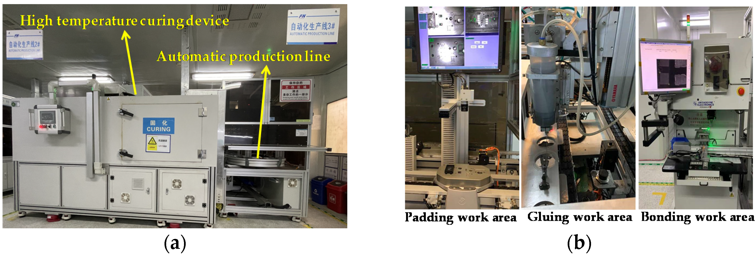
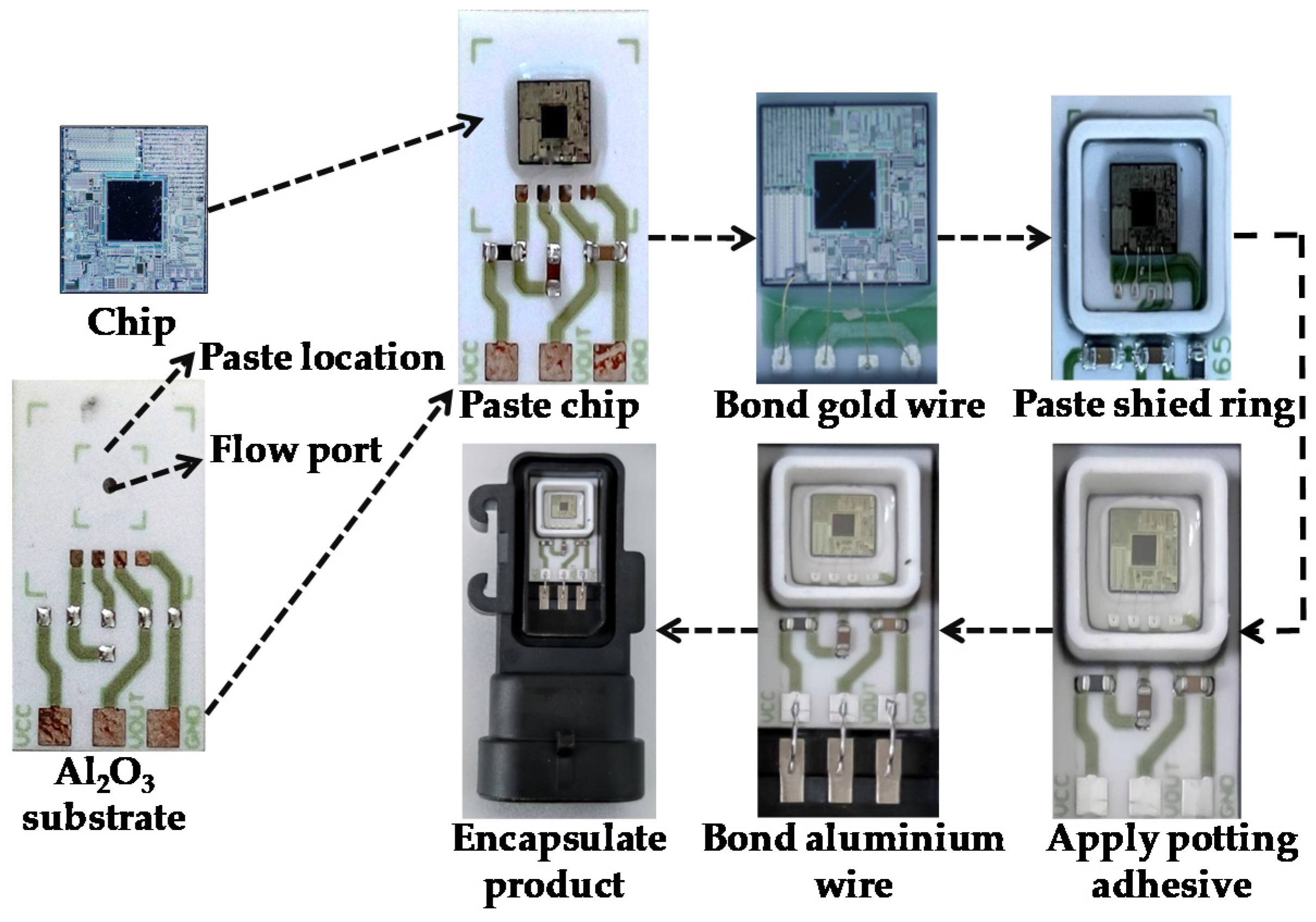
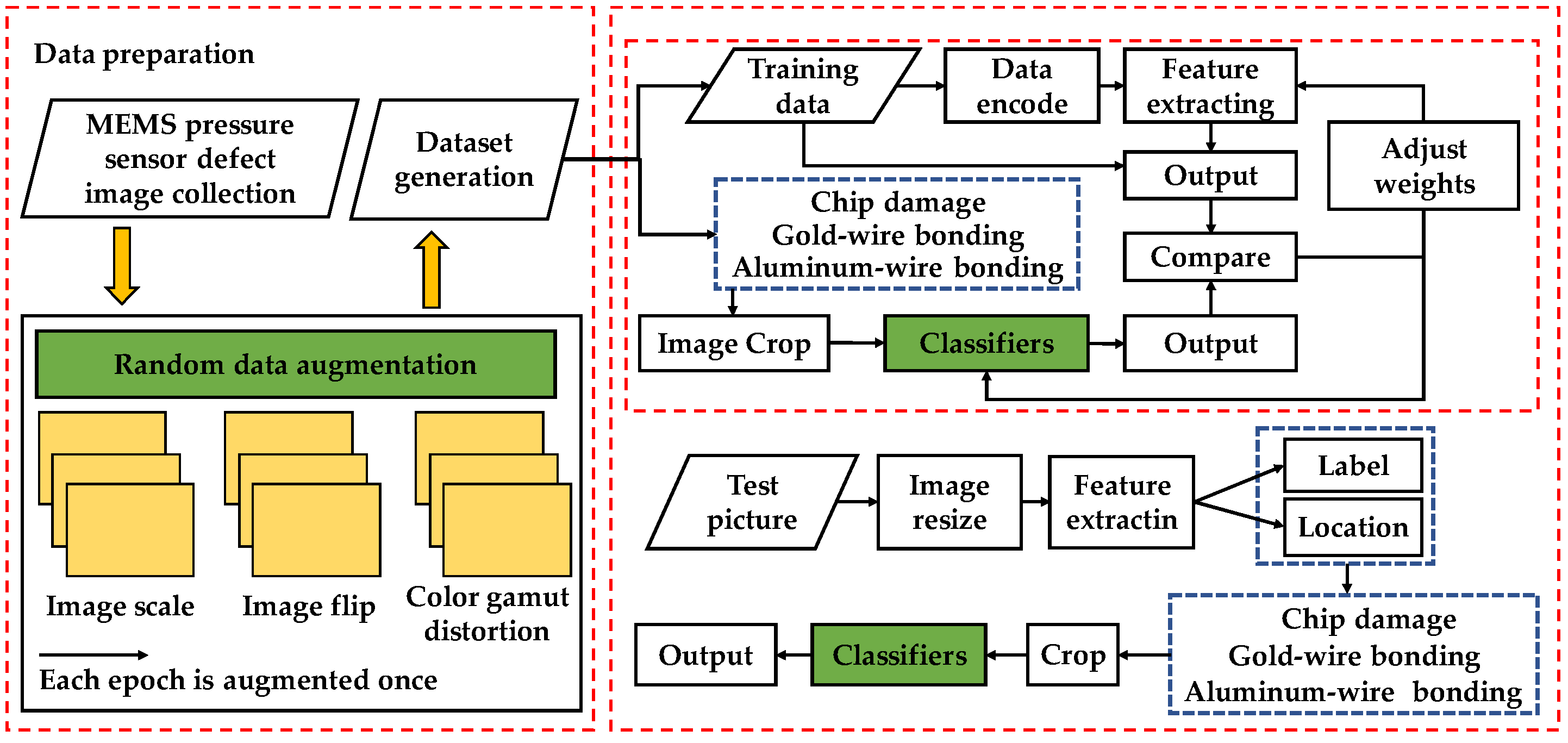
2. System Overview
3. Proposed CNN
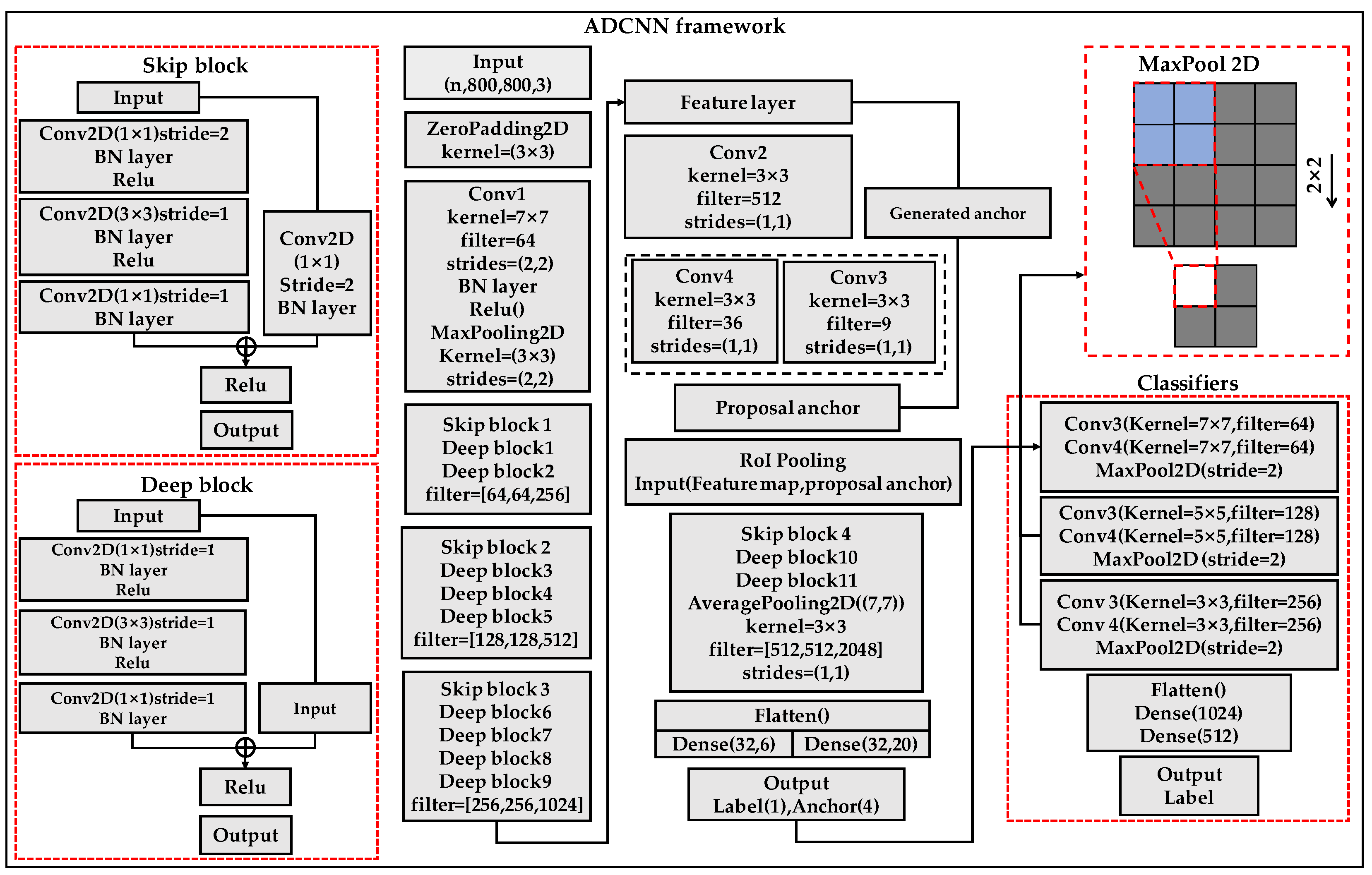
3.1. Improved Network Framework
3.2. Workflow of the Network
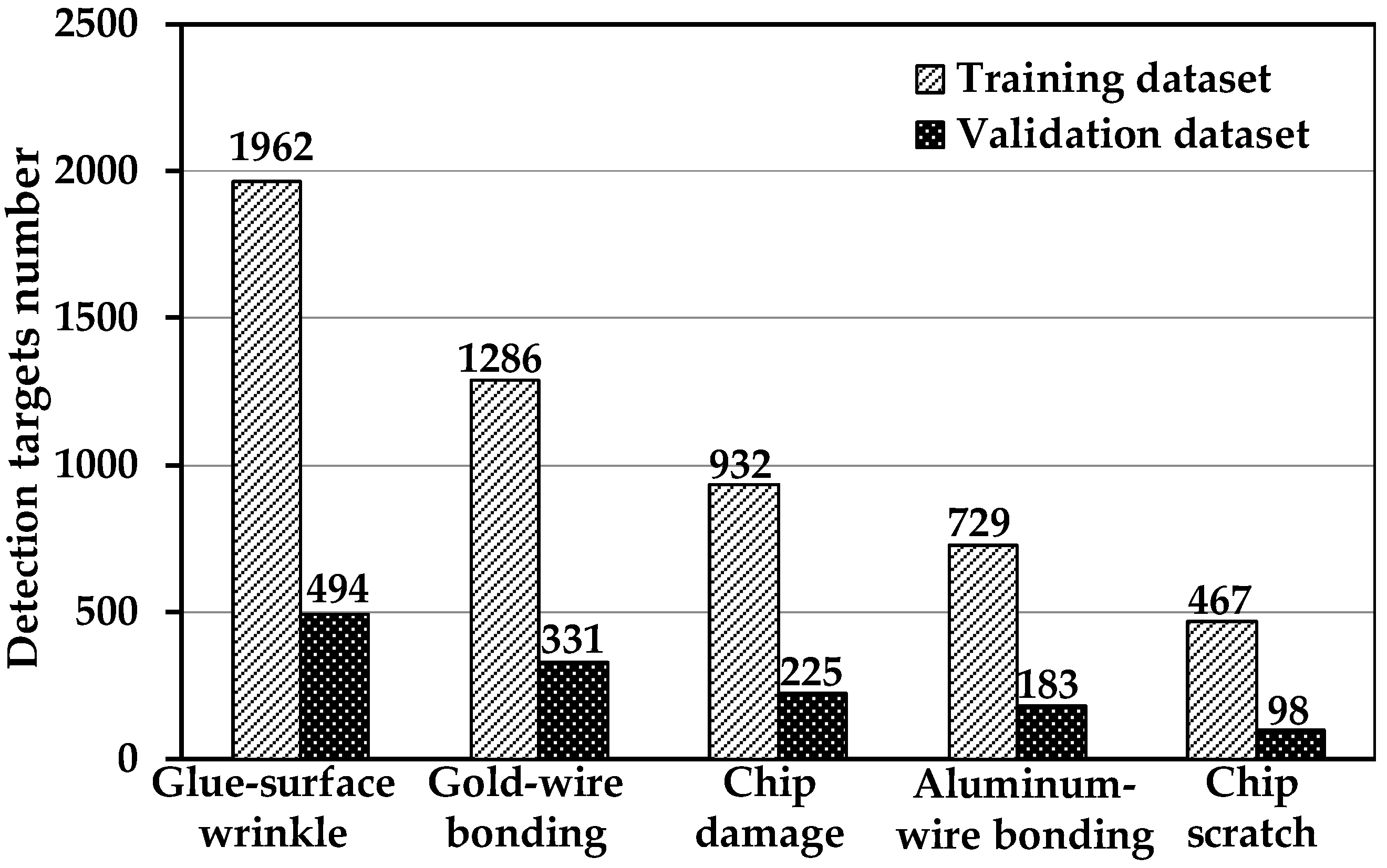
4. Training and Validation
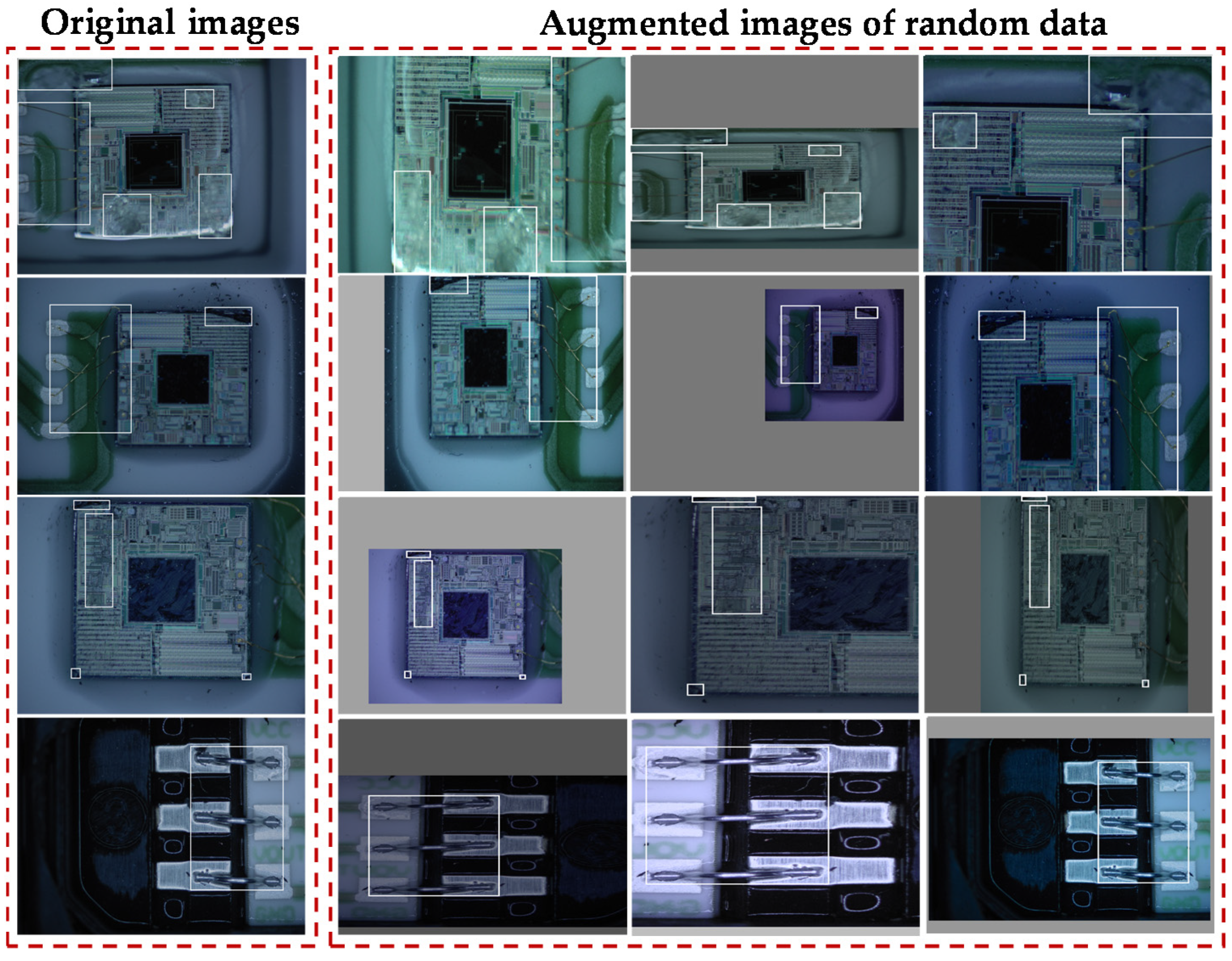
4.1. Data Augmentation
4.2. Training Method
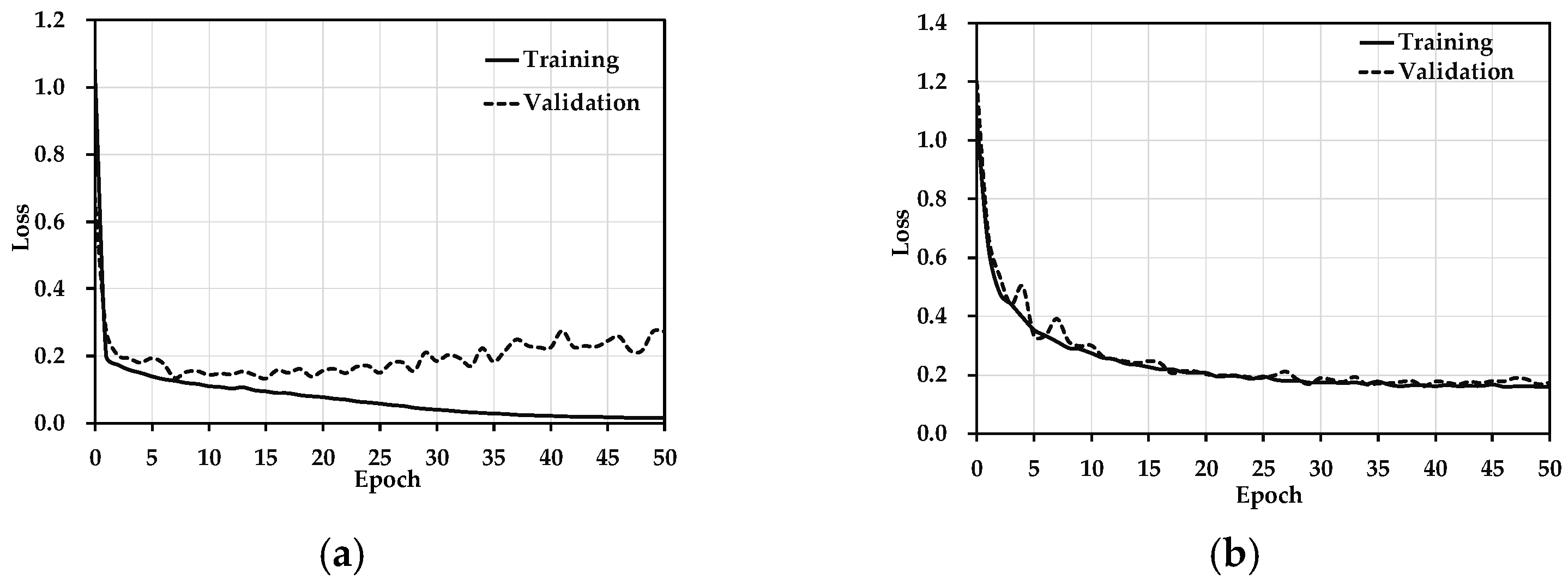
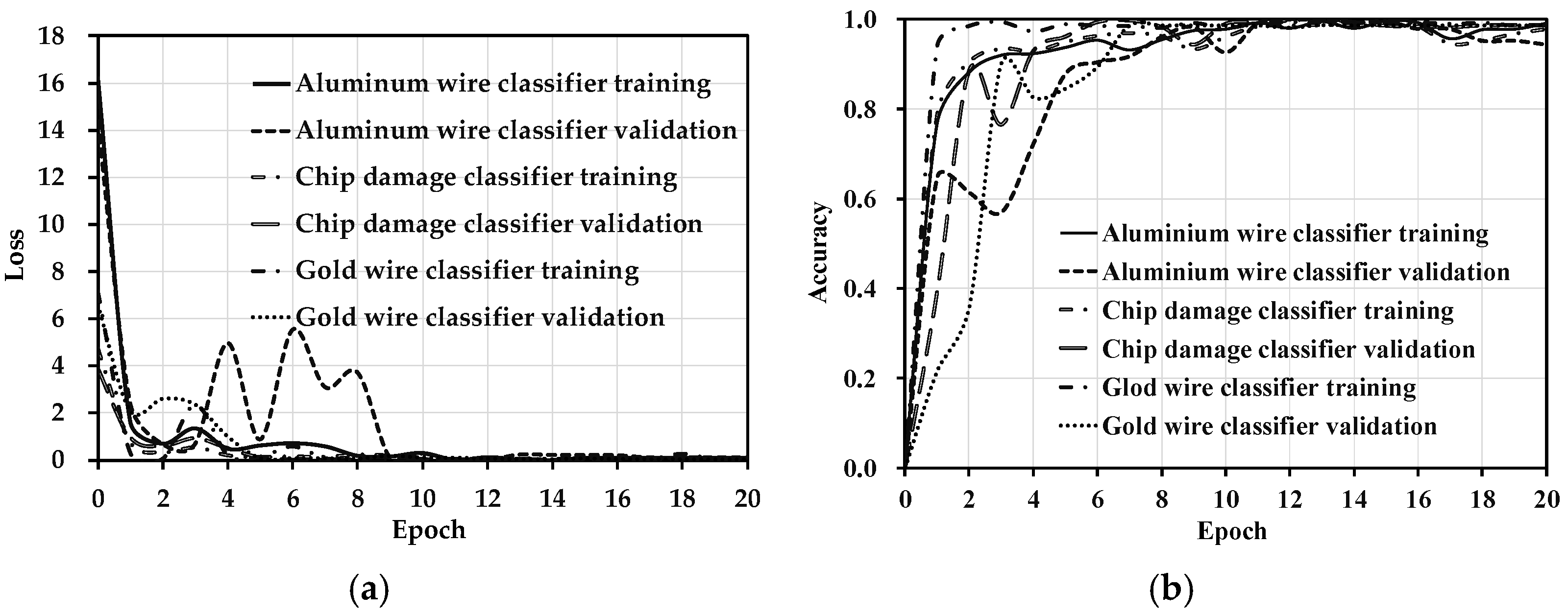
4.3. Training Results
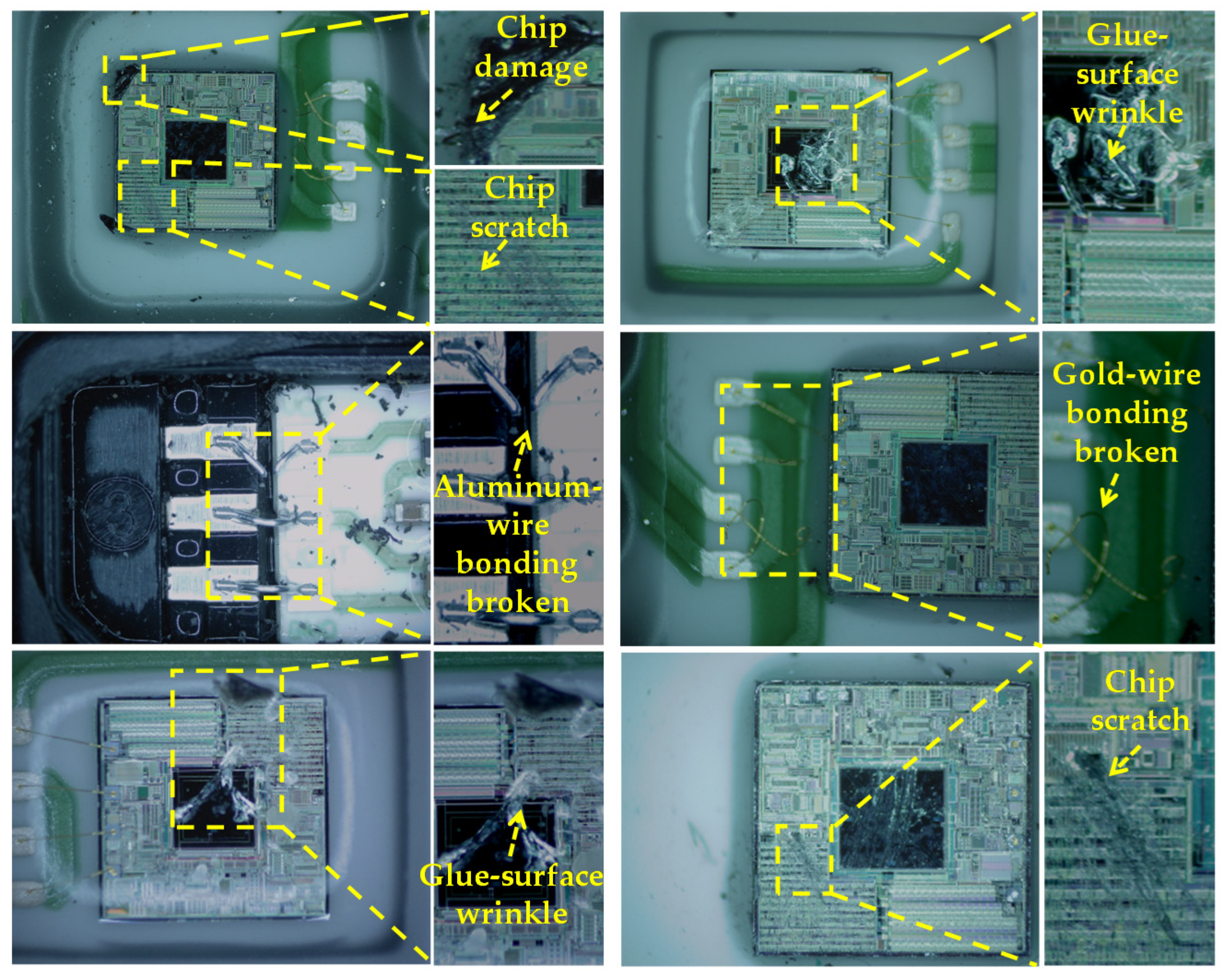
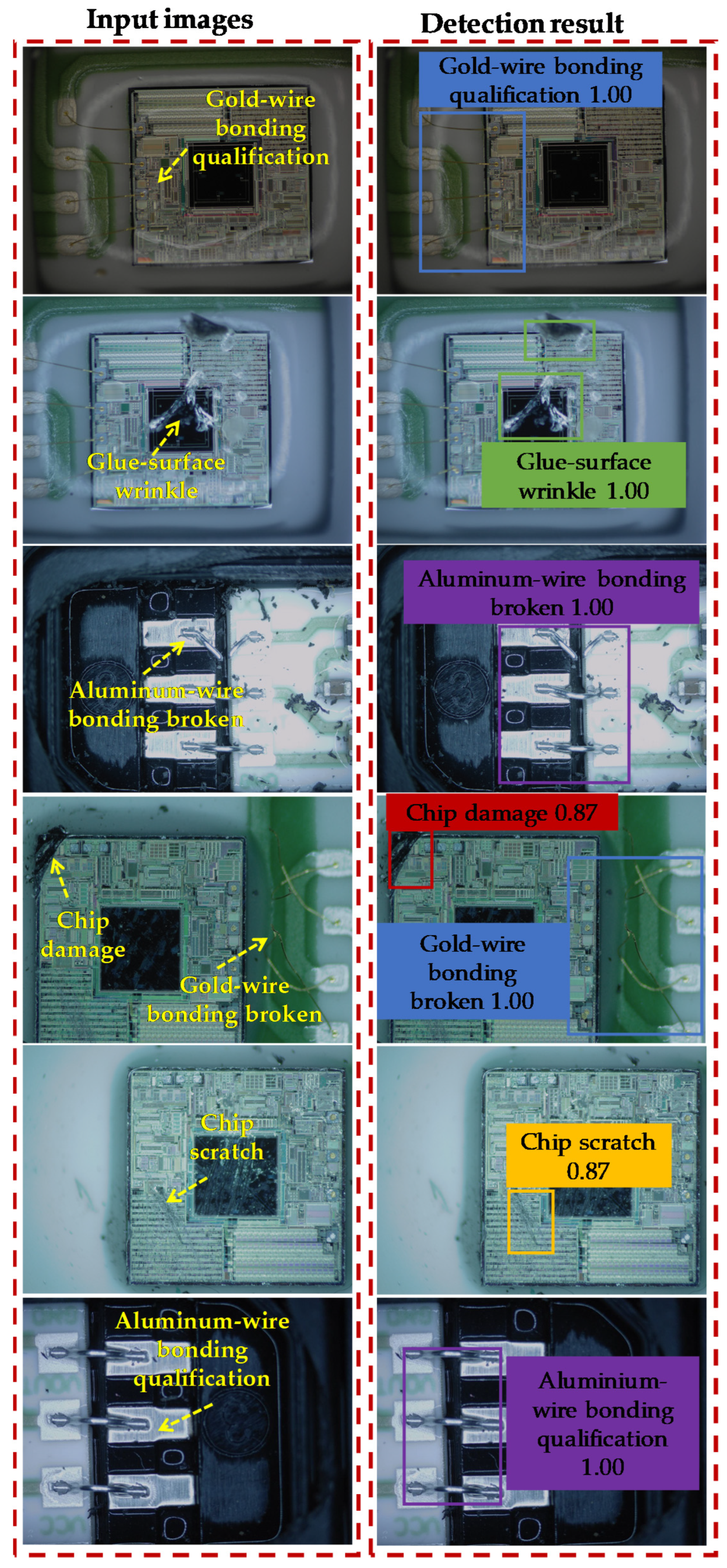
5. MEMS Defect Detection
6. Conclusions
Author Contributions
Funding
Institutional Review Board Statement
Informed Consent Statement
Data Availability Statement
Conflicts of Interest
References
- Ahmad, F.; Baig, A.; Dennis, J.; Hamid, N.; Khir, M. Characterization of MEMS comb capacitor. Microsyst. Technol. 2020, 26, 1387–1392. [Google Scholar] [CrossRef]
- Zhang, Y.; Li, B.; Li, H.; Shen, S.; Li, F.; Ni, W.; Cao, W. Investigation of potting adhesive induced thermal stress in MEMS pressure sensor. Sensors 2021, 21, 2011. [Google Scholar] [CrossRef] [PubMed]
- Hafez, N.; Haas, S.; Loebel, U.; Reuter, D.; Ramsbeck, M.; Schramm, M.; Horstmann, J.; Otto, T. Characterisation of MOS transistors as an electromechanical transducer for stress. Phys. Status Solidi 2019, 216, 1700680. [Google Scholar] [CrossRef]
- Gao, T.; Sheng, W.; Zhou, M.; Fang, M.; Luo, F.; Li, J. Method for fault diagnosis of temperature-related MEMS inertial sensors by combining hilbert-huang transform and deep learning. Sensors 2020, 20, 5633. [Google Scholar] [CrossRef] [PubMed]
- Basov, M. Development of high-sensitivity pressure sensor with on-chip differential transistor amplifier. J. Micromechanics Microeng. 2020, 30, 065001. [Google Scholar] [CrossRef]
- Yu, Z.; Zhao, Y.; Sun, L.; Tian, B.; Jiang, Z. Incorporation of beams into bossed diaphragm for a high sensitivity and overload micro pressure sensor. Rev. Sci. Instrum. 2013, 84, 015004. [Google Scholar] [CrossRef]
- Xu, T.; Lu, D.; Zhao, L.; Jiang, Z.; Wang, H.; Guo, X.; Zhao, Y. Application and optimization of stiffness abruption structures for pressure sensors with high sensitivity and anti-overload ability. Sensors 2017, 17, 1965. [Google Scholar] [CrossRef] [PubMed]
- Basov, M.; Prigodskiy, D. Investigation of high-sensitivity piezoresistive pressure sensors at ultra-low differential pressures. IEEE Sens. J. 2020, 20, 7646–7652. [Google Scholar] [CrossRef]
- Basov, M. Ultra-high sensitivity MEMS pressure sensor utilizing bipolar junction transistor for pressures ranging from −1 to 1 kPa. IEEE Sens. J. 2020, 21, 4357–4364. [Google Scholar] [CrossRef]
- Asgary, R.; Mohammadi, K.; Zwolinski, M. Using neural networks as a fault detection mechanism in MEMS devices. Microelectron. Reliab. 2007, 47, 142–149. [Google Scholar] [CrossRef]
- LeCun, Y.; Bengio, Y.; Hinton, G. Deep learning. Nature 2015, 521, 436–444. [Google Scholar] [CrossRef] [PubMed]
- Lecun, Y.; Bottou, L.; Bengio, Y.; Haffner, P. Gradient-based learning applied to document recognition. Proc. IEEE 1998, 86, 2278–2324. [Google Scholar] [CrossRef]
- Simonyan, K.; Zisserman, A. Very deep convolutional networks for large-scale image recognition. arXiv 2014, arXiv:1409.1556. [Google Scholar]
- Szegedy, C.; Liu, W.; Jia, Y.; Sermanet, P.; Reed, S.; Anguelov, D.; Erhan, D.; Vanhoucke, V.; Rabinovich, A. Going deeper with convolutions. In Proceedings of the IEEE Conference on Computer Vision and Pattern Recognition (CVPR), Boston, MA, USA, 8–10 June 2015; pp. 1–9. [Google Scholar]
- Krizhevsky, A.; Sutskever, I.; Hinton, G. Imagenet classification with deep convolutional neural networks. Adv. Neural Inf. Process. Syst. 2017, 60, 84–90. [Google Scholar] [CrossRef]
- Zeiler, M.; Fergus, R. Visualizing and Understanding Convolutional Neural Networks; Springer International Publishing: Cham, Switzerland, 2013; pp. 818–833. [Google Scholar]
- Szegedy, C.; Ioffe, S.; Vanhoucke, V.; Alemi, A. Inception-v4, inception-resnet and the impact of residual connections on learning. In Proceedings of the Thirty-First AAAI Conference on Artificial Intelligence, San Francisco, CA, USA, 4–9 February 2017; pp. 4278–4284. [Google Scholar]
- Huang, G.; Liu, Z.; Maaten, L.; Weinberger, K. Densely connected convolutional networks. In Proceedings of the IEEE Conference on Computer Vision and Pattern Recognition (CVPR), Honolulu, HI, USA, 22–25 July 2017; pp. 2261–2269. [Google Scholar]
- Hu, J.; Shen, L.; Albanie, S.; Sun, G.; Wu, E. Squeeze-and-excitation networks. In Proceedings of the IEEE Conference on Computer Vision and Pattern Recognition, Seattle, WA, USA, 14–19 June 2020; pp. 2011–2023. [Google Scholar]
- Howard, A.; Zhu, M.; Chen, B.; Kalenichenko, D.; Wang, W.; Weyand, T.; Andreetto, M.; Adam, H. MobileNets: Efficient convolutional neural networks for mobile vision applications. arXiv 2017, arXiv:1704.04861. [Google Scholar]
- Zhang, X.; Zhou, X.; Lin, M.; Sun, J. ShuffleNet: An extremely efficient convolutional neural network for mobile devices. In Proceedings of the IEEE Conference on Computer Vision and Pattern Recognition (CVPR), Salt Lake City, UT, USA, 18–22 June 2018; pp. 6848–6856. [Google Scholar]
- Xie, S.; Girshick, R.; Dollár, P.; Tu, Z.; He, K. Aggregated residual transformations for deep neural networks. In Proceedings of the IEEE Conference on Computer Vision and Pattern Recognition (CVPR), Honolulu, HI, USA, 22–25 July 2017; pp. 5987–5995. [Google Scholar]
- Sandler, M.; Howard, A.; Zhu, M.; Zhmoginov, A.; Chen, L. MobileNetV2: Inverted residuals and linear bottlenecks. In Proceedings of the IEEE Conference on Computer Vision and Pattern Recognition (CVPR), Salt Lake City, UT, USA, 18–22 June 2018; pp. 4510–4520. [Google Scholar]
- Mehta, S.; Rastegari, M.; Caspi, A.; Shapiro, L.; Hajishirzi, H. ESPNet: Efficient spatial pyramid of dilated convolutions for semantic segmentation. In Proceedings of the European Conference on Computer Vision (ECCV), Munich, Germany, 8–14 September 2018; pp. 552–568. [Google Scholar]
- Ma, N.; Zhang, X.; Zheng, H.; Sun, J. ShuffleNet v2: Practical guidelines for efficient CNN architecture design. In Proceedings of the European Conference on Computer Vision (ECCV), Munich, Germany, 8–14 September 2018; pp. 116–131. [Google Scholar]
- Mehta, S.; Rastegari, M.; Shapiro, L.; Hajishirzi, H. ESPNetv2: A light-weight, power efficient, and general purpose convolutional neural network. In Proceedings of the IEEE Conference on Computer Vision and Pattern Recognition (CVPR), Los Angeles, CA, USA, 16–20 June 2019; pp. 9182–9192. [Google Scholar]
- Ren, S.; He, K.; Girshick, R.; Sun, J. Faster R-CNN: Towards real-time object detection with region proposal networks. Adv. Neural Inf. Process. Syst. 2015, 39, 1137–1149. [Google Scholar] [CrossRef] [PubMed]
- Redmon, J.; Divvala, S.; Girshick, R.; Farhadi, A. You only look once: Unified, real-time object detection. In Proceedings of the IEEE Conference On Computer Vision and Pattern Recognition (CVPR), Las Vegas, NV, USA, 29–30 June 2016; pp. 779–788. [Google Scholar]
- He, Y.; Song, K.; Meng, Q.; Yan, Y. An end-to-end steel surface defect detection approach via fusing multiple hierarchical features. IEEE Trans. Instrum. Meas. 2020, 69, 1493–1504. [Google Scholar] [CrossRef]


| Detection Classes | Recall (%) | Precision (%) | AP (%) | MAP (%) |
|---|---|---|---|---|
| Chip scratch | 100.0 | 95.2 | 98.2 | 89.6 |
| Chip damage | 94.5 | 60.9 | 65.8 | |
| Gold-wire bonding | 99.7 | 98.2 | 99.7 | |
| Glue-surface wrinkles | 82.0 | 98.8 | 84.3 | |
| Aluminum-wire bonding | 100.0 | 100.0 | 100.0 |
| Detection Classes | Recall (%) | Precision (%) | AP (%) | MAP (%) |
|---|---|---|---|---|
| Chip scratch | 96.1 | 86.8 | 92.3 | 92.4 |
| Chip damage | 80.0 | 75.8 | 71.5 | |
| Gold-wire bonding | 98.3 | 82.7 | 98.8 | |
| Glue-surface wrinkles | 88.1 | 93.5 | 95.4 | |
| Aluminum-wire bonding | 100.0 | 100.0 | 100.0 |
| Network | AP/% | MAP /% | Single-Picture Detection Time/ms | ||||
|---|---|---|---|---|---|---|---|
| Chip Scratch | Chip Damage | Gold-Wire Bonding | Glue-Surface Wrinkles | Aluminum-Wire Bonding | |||
| Faster RCNN | 90.5 | 89.6 | 93.5 | 85.7 | 89.9 | 89.8 | 51 |
| YOLOv3 | 85.4 | 79.9 | 83.0 | 87.6 | 81.8 | 83.0 | 45 |
| YOLOv4 | 92.8 | 82.7 | 95.5 | 93.2 | 92.4 | 91.3 | 42 |
| ADCNN (This work) | 92.3 | 91.2 | 98.8 | 95.4 | 98.4 | 92.4 | 68 |
Publisher’s Note: MDPI stays neutral with regard to jurisdictional claims in published maps and institutional affiliations. |
© 2022 by the authors. Licensee MDPI, Basel, Switzerland. This article is an open access article distributed under the terms and conditions of the Creative Commons Attribution (CC BY) license (https://creativecommons.org/licenses/by/4.0/).
Share and Cite
Deng, M.; Zhang, Q.; Zhang, K.; Li, H.; Zhang, Y.; Cao, W. A Novel Defect Inspection System Using Convolutional Neural Network for MEMS Pressure Sensors. J. Imaging 2022, 8, 268. https://doi.org/10.3390/jimaging8100268
Deng M, Zhang Q, Zhang K, Li H, Zhang Y, Cao W. A Novel Defect Inspection System Using Convolutional Neural Network for MEMS Pressure Sensors. Journal of Imaging. 2022; 8(10):268. https://doi.org/10.3390/jimaging8100268
Chicago/Turabian StyleDeng, Mingxing, Quanyong Zhang, Kun Zhang, Hui Li, Yikai Zhang, and Wan Cao. 2022. "A Novel Defect Inspection System Using Convolutional Neural Network for MEMS Pressure Sensors" Journal of Imaging 8, no. 10: 268. https://doi.org/10.3390/jimaging8100268