Review

Interacting with Futuristic Topological Quantum Materials: A Potential Candidate for Spintronics Devices

1
Special Centre for Nanoscience, Jawaharlal Nehru University, Munirka, New Delhi 110067, India
2
Department of Electronic Science, University of Delhi, South Campus, South Moti Bagh, New Delhi 110021, India
3
Shaheed Rajguru College of Applied Science for Women, Vasundhara Enclave, New Delhi 110096, India
4
Ramjas College, University Enclave, Delhi 110007, India
5
Department of Chemistry, Gurukula Kangri (Deemed to Be University), Haridwar 249404, India
6
Department of Chemistry, Sri Venkateswara College, University of Delhi, Dhaula Kuan Enclave 1, New Delhi 110021, India
*
Authors to whom correspondence should be addressed.
Magnetochemistry 2023, 9(3), 73; https://doi.org/10.3390/magnetochemistry9030073
Submission received: 19 December 2022 / Revised: 24 February 2023 / Accepted: 26 February 2023 / Published: 2 March 2023
(This article belongs to the Special Issue Spin and Charge Transport in Novel Quantum and Topological Materials)

Abstract

:
Spintronics, also known as magneto-electronics or spin transport electronics, uses the magnetic moment of the electron due to intrinsic spin along with its electric charge. In the present review, the topological insulators (2D, 3D, and hydride) were discussed including the conducting edge of 2D topological insulators (TIs). Preparation methods of TIs along with fundamental properties, such as low power dissipation and spin polarized electrons, have been explored. Magnetic TIs have been extensively discussed and explained. Weyl phases, topological superconductors, and TIs are covered in this review. We have focused on creating novel spintronic gadgets based on TIs which have metallic topological exterior facades that are topologically defended and have an insulating bulk. In this review, topological phases are discussed as a potential candidate for novel quantum phenomena and new technological advances for fault-tolerant quantum computation in spintronics, low-power electronics, and as a host for Majorana fermions are elucidated. Room temperature stable magnetic skyrmions and anti-skyrmions in spintronics for next-generation memory/storage devices have been reported.

1. Introduction

The advanced condensed matter physics gained popularity in research over the last century, mainly due to the Ginzburg–Landau paradigm (Ginzburg and Landau, 1950) and the assumption model for the theory of spontaneous symmetry breaking. Maximum complexity for superconductivity, quantum magnetism, super fluidity, and soft matter can be easily seen in their paradigm. Much work has been done to comprehend and regulate this topologically unique quantum state when the quantum Hall (QH) state was discovered [1,2]. It is shown that, on a 2D (two dimension)-based sample with an insulating bulk, electric current flows along its edges [3].
TIs are unique substances different from the typically three types of solid materials: conductors, insulators, and semiconductors [4] (Figure 1). The mobility of free electrons is independent of the band separation crossing. Because of the large separation between occupied and unoccupied states, an insulator cannot conduct electricity. Energy must be taken up by the electron in order to make a jump from the maximum occupied energy to the least occupied energy state. The band gap of the semiconductor is between that of the conductor and the insulator as shown in Figure 1. However, the TIs defy easy categorization within any of these groups. TIs possess bulk electronic states with a tiny band gap, indicating that the bulk states do not contain free carriers. However, they also have metallic surfaces that are topologically shielded. A Dirac point Figure 1 that can cross the band gap is present in this gapless surface state, proving that the TI surface is conductive [5] and a unique surface state as a result of T-symmetry and high order spin orbit coupling (SOCs) in its interior is produced. This clearly indicates that TIs can minimize or eliminate the dispersion of non-magnetic contamination [6].
A recently identified electronic phase called TIs has a conducting surface but an insulating bulk [3,7]. In contrast to superconductors and magnets, a TIs has a topological order that is conserved by T-symmetry. Achieving high mobility; non-dissipative electrical transmission is a highly attractive target for devices. However, TIs can also be seen in the nonmagnetic field, which is a significant difference from the QH state. However, TIs can also be seen in the non-magnetic field, which is a significant distinction from the QH state. A magnetic field is induced during electron motion in 2D TIs due to spin-orbit interaction with heavy metals such as Hg and Bi. This is called the quantum spin Hall (QSH) state and was first demonstrated in 2006 in HgTe quantum wells [8,9]. More than a decade passed, yet research on TIs continued unabated. The TI’s QSH states are stable at room temperature, giving it practical and technical importance. Preparation, doping, and studies of electric as well as magnetic properties are further possible areas of investigation. However, there is still a problem in controlling the Fermi level in synthesized TIs, and mass production of TIs for practical and industrial application is also a setback. Since TI was discovered much later, several metrics, such as electronic mobility, are lower than their theoretically predicted value. However, these investigations are driven by the desire to learn more about TI’s remarkable properties before they are used in engineering and other applied contexts. Currently, TI research is still at an early stage. Researchers and scientists are working to increase the efficiency of TIs-based products.

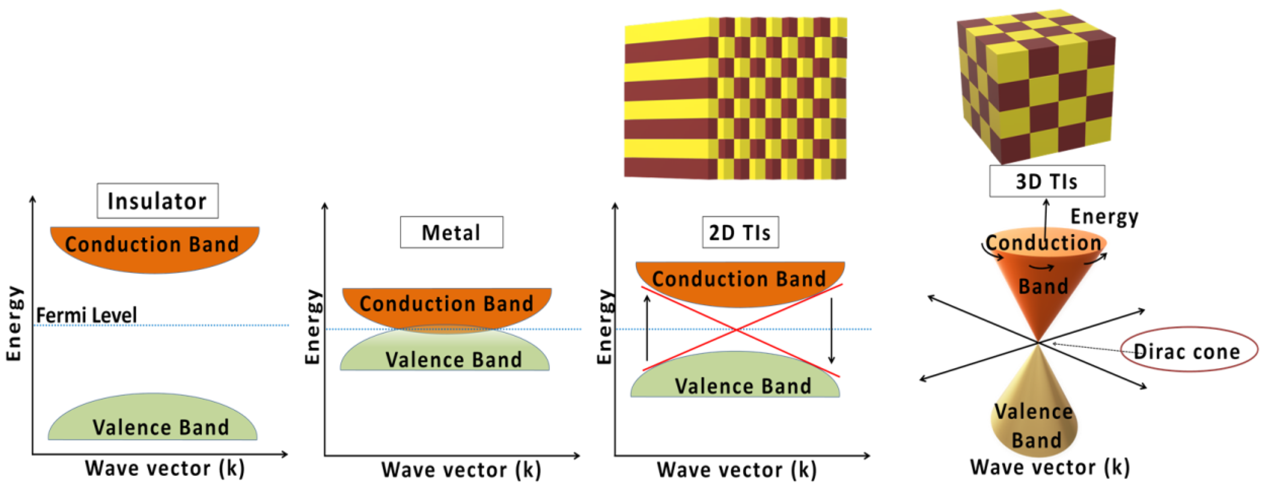
2. Classification of TIs

The TIs can be categorized in very different ways based on the basic dimensions of the TIs, the parity of the Dirac point, the strong TIs, the weak TIs, the hybrid TIs, the induced magnetic based TIs, and the last classification by symmetry (Table 1). HfTe5 and ZrTe5 bulk materials have a significant gap with a monolayer. TIs is a 2D quantum well structure of HgCdTe. In comparison, the stoichiometry and chemical phase of 3D TIs are more stable and show more promising properties. The second is organized according to Dirac point parity. The last one will focus on geometry-based symmetry.

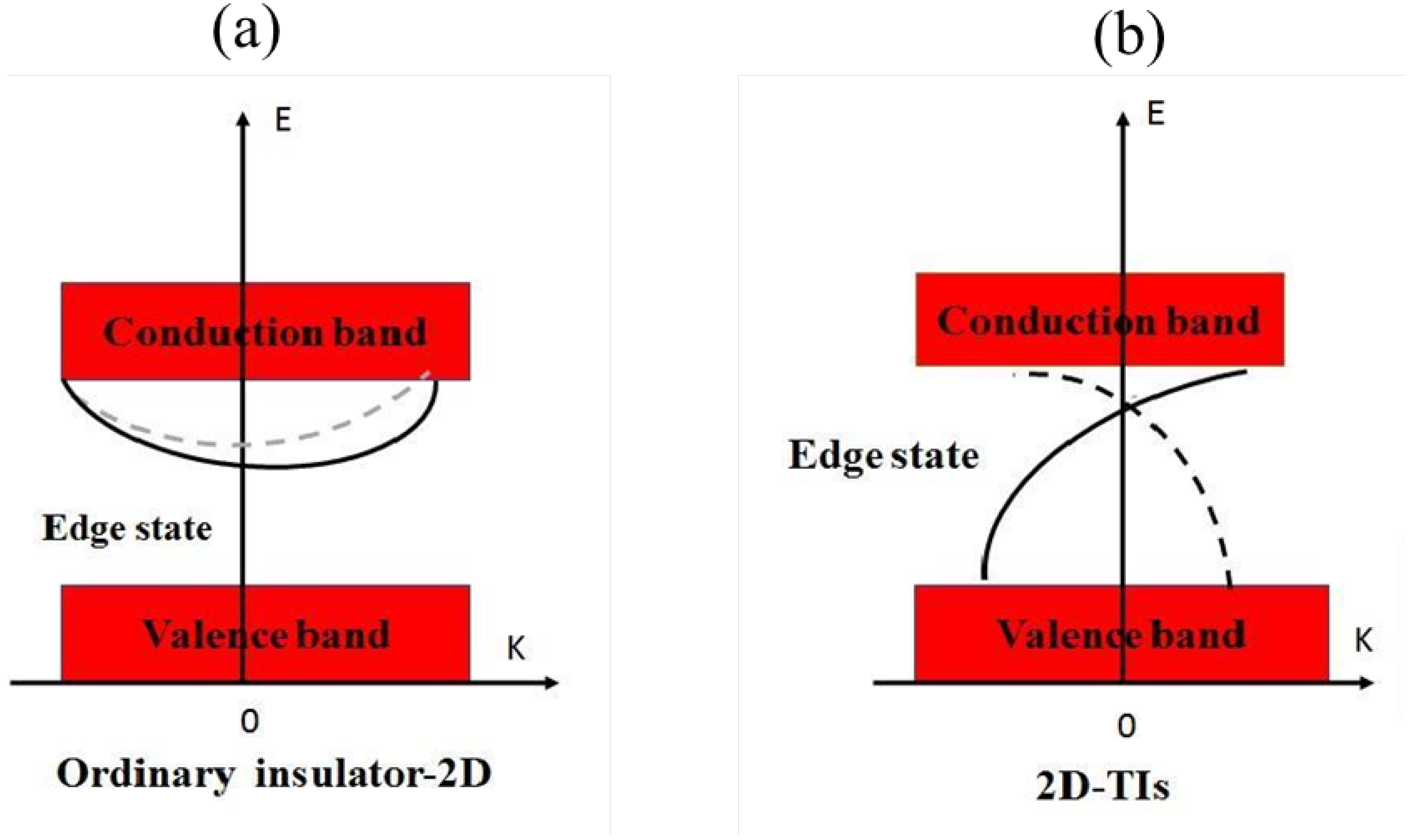
2.1. Two-Dimensional TIs

In 2D systems, Figure 2 Thouless and Kosterlitz investigated a novel phase transition in 1972 [48]. In 1982, Thouless et al. used the principles of topological interpretation to present how Hall conductivity quantization states play a clear role in the 2D electron gas model, acting as topological defects and formally known as the Thouless–Kohmoto–Nightingale (TKN) number, resulting in a peculiarity at TIs [48]. Due to the low spin-orbit coupling of graphene, the QSH effect has not yet been directly verified experimentally, although it is one of the most anticipated 2D TIs (SOCs) [49]. Increasing the SOCs effect is essential for fundamental studies and potential applications of graphene-based QSH insulators. According to studies, one way to increase graphene’s SOCs is to heavily dope it with adatoms or to lay it on substrates with robust SOCs connections, as shown in Figure 2. Recently, interest in investigating non-trivial topologies has been sparked by the prospect of finding room-temperature QSH insulators in 2D transition metal dichalcogenides (TMDs) [50].
Single-layer 1T’ Wte2 is a stable QSH insulator, according to experimental evidence, but the QSH phase lasts for only 100K. Consequently, QSH phases are only seen in a limited number of pristine 2D TMDs. So, it is important to address additional variations outside of binary TMDs [52].

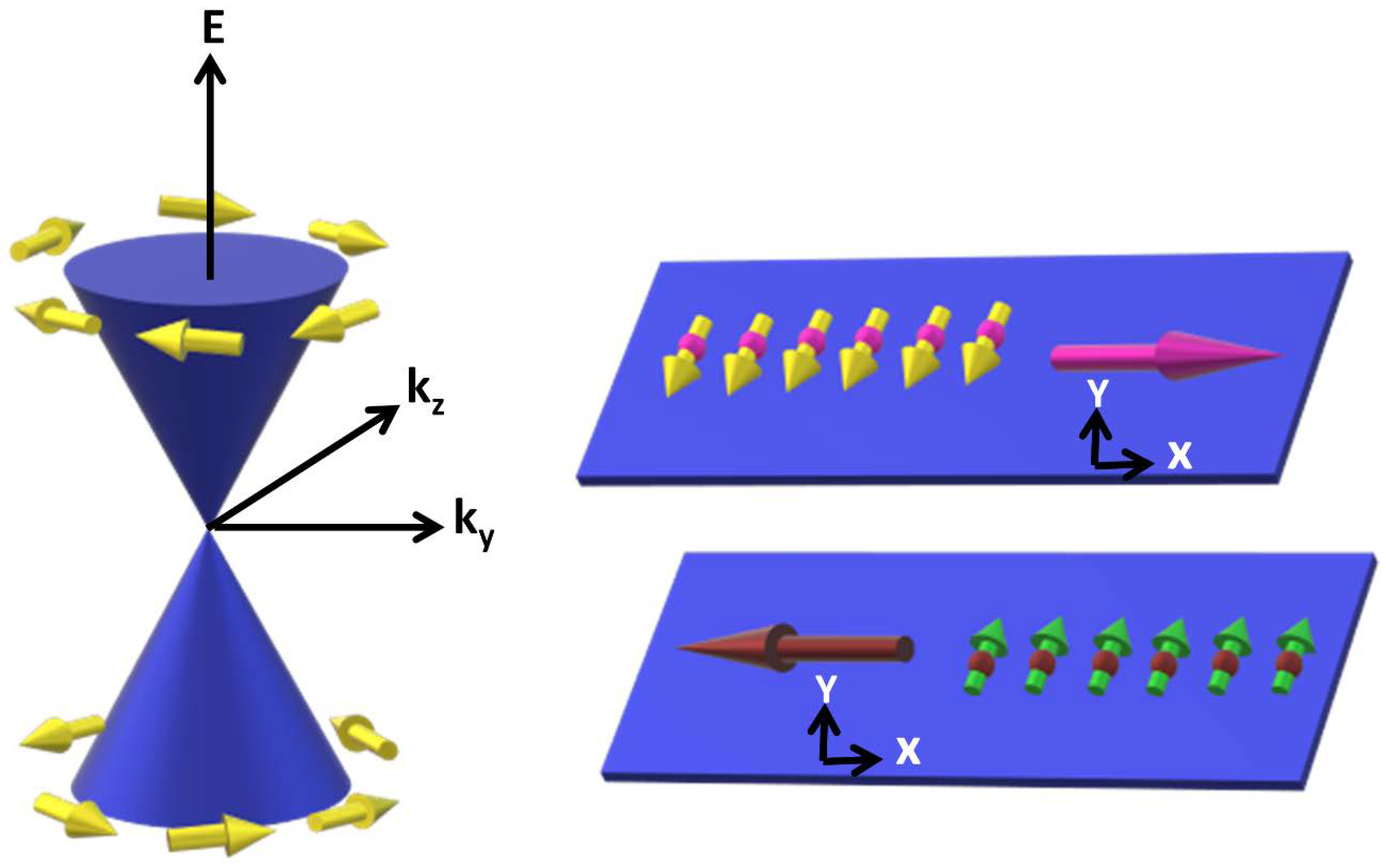
2.2. Conducting Edge Sates for 2D TIs

Most often, 2D TIs follow a unique conductor pattern, conducting along their edges because of this property of bulk isolation. They can be characterized in two different ways, such as a bulk topological invariant (Z2 index for the QSH-type insulator and the Chern number for quantum anomalous Hall effect (QAHE), and 2D TIs character edges state, where QSH states are defined as helical for quantum anomalous Hall effect (QAHE). Two topologically distinct insulators, the Semenov phase and the Haldane phase, have metallic edge states with topological protection if the bulk gaps are preserved. The illustration is shown in 2D (Figure 3) and the 1D interface is where the edge modes work [53]. TIs have novel quantum material states that are adiabatically separated from traditional dielectric and semi-electrics. The bulk part of TI has a complete insulating gap, and time-reversal symmetry protects the presence of any gapless edge or surface. BiSb alloys, HgTe quantum wells, Bi2Te3 and Bi2Se3 crystals, and other systems have been theoretically predicted and the existence of these topological materials confirmed experimentally. Theoretical models, material properties, and experimental results are checked on 2D and 3D TIs. Topological superconductors have Majorana fermions in the bulk’s full pairing gap and bulk surface states. In the present work, the topological superconductor (TSCs) theory is examined in close analogy to the TIs.
In Figure 4, it can be seen that a semi-infinite plane of a 2D body illustrates the differences in edges value between traditional and TIs. Since it is assumed that there is translational symmetry along the edge of the semi-infinite plane, the wavenumber k for the Bloch function is a best-chosen quantum number beside the direction [54]. Figure 4a,b show edge state diagrams for ordinary insulators and TIs, respectively. The differences in the connections between edge states and valence or conduction bands were also observed. Edge-state scattering in TIs is related to both the bulk valence band (VB) and conduction band (CB), in contrast to conventional insulators where it is related to the same bulk bands on both sides. From Figure 4a,b, it can be seen that SOCs cause the edge states to be spin-split, or Rashba split. The edge states with the opposite rotations and symmetries with respect to k = 0 are Kramers degenerate according to the time-reversal symmetry. Note that the bulk gap cannot be closed without continuously deforming Figure 4a,b into each other. This is given if the T-symmetry is preserved. Figure 4a,b show the simplest scenarios, but other types of edge states can also be considered. Non-magnetic insulators with edge states can be classified as topological and ordinary resistors can be identified by counting the Fermi energy’s edge states using Kramers pairs of states. The TIs (ν = 1) and the ordinary insulator (ν = 0) then give the number of pairings by calculating the number of edge states via the Fermi energy for insulators, each depending on how much Fermi energy is contained in the distance Figure 4a is either two or zero, while the value in Figure 4b is one. If the bulk gap does not close, ν will not be this topological number as parameters are continuously changed. Upon the eventual closure of the bulk gap, the topological number might change. By changing the parameters, it can be shown how bulk gap decreases and this classification can be related to a change in topological number.

2.3. Three-Dimensional TIs

The spin QHE observed in HgTe quantum wells is caused by the 3D topological invariant. The term “topological insulators” was created because the 3D phases are topological in the same sense as the IQHE, with topologically protected edges or surface states (SSs) originating from SOCs rather than a magnetic field. All known 3D TIs have so far been identified using angle-resolved light emission spectroscopy, which examines the respective metallic SSs and subsequently the topological invariants. By changing the variables, one can categories how the bulk gap shrinks and associate this categorization with a change in the topological number. It was observed that topological and usual phase diagrams of insulators showed some similarities. Lin et al. proposed topological invariants for a general T-invariant band insulator [55]. Topological invariants, which in this context are integrals over a band structure are fundamentally mathematical quantities. They do not change if parameters are changed over and over again. The simpler versions of these invariants in inversion symmetric materials were discovered independently, and they were used to predict the discovery of the first TIs, BixSb1−x [29]. More forms of data are now available due to the variety of probes that can be used to evaluate 3D TIs. TIs have been linked to many different areas of condensed matter physics through theoretical studies and TIs have been found in a variety of different types of materials.
One of the new generations of TIs is known as topological crystalline insulators (TCIs), and represents the third generation. Liu et al. [56] calculated the band gap structure and performed topological band analysis to develop TCIs in 2013. Likewise, its interior was characterized by a band gap, while its outside was home to a boundary state with spin filtering capabilities and was shielded by mirror symmetry (001). Its mirror symmetry of the lattice preserved an even number of Dirac cones rather than its T-symmetry. This unique topological phase has been realized in SnTe and PbxSn1−xSe (Te) films (001). Third generation TIs have an adjustable band gap that sets them apart from previous generations. In order to change the film parallel to the electric field and subsequently the edge state’s band gap, the system’s mirror symmetry must be broken. That was not the case at all with the second-generation TI, which featured a number of surface states. The solitary Dirac cone is one of the typical surface states of 3D TIs (Figure 5).

2.4. Hybrid TIs

To exploit their new properties, one can fabricate different types of hybrid structures using TIs. For instance, remarkable magneto-transport behavior has been theoretically predicted for hybrid TI ferromagnetic hybrid structures (Figure 6) resulting in unusual spin-based momentum locking on the TIs’ surface [58]. A recent advance in this direction is the effective development of the ferro insulator EuS on Bi2Se3. One could also produce and control Majorana fermions by combining a TI, the best conductor, and a ferro type insulator. In the last decade, a mixture of reverse-symmetry-breaking operations has been discovered in magnetic-topological quantum physics. Compared to the uniformly thin film nanomaterials, the MTIs heterostructure (Figure 6) provides a more stable framework to alter quantum mechanical phenomena, such as spin-orbit coupling and spin/magnetic possession (Bi,Sb)2(Te,Se)3 type hybrid magnetic TIs. In the field of condensed-matter physics, materials science, topological phases, such as the traditional unit-rank and above unit rank TIs and semimetals, have become a booming topic. A topological insulator typically exhibits a fixed-order topological invariant as well as a correspondence over linked bulk-boundaries.
Here, a novel topological insulator, termed hybrid-order TI, is recognized in a two-layer photonic crystal that simultaneously supports first- and second-order topologies. In the same system, zero-dimensional corner states and 1-D without gap helical edge states coexist. The new hybrid-order topological phase might result in inventive topological acoustic device applications.

3. Properties and Characteristics of TIs

3.1. Low Power Dissipation

Low power dissipation is good characteristic of TI in addition to its high mobility. The presence of band gaps in an insulator causes resistance, while other factors cause resistance in a metal when electrons and phonons, impurities, and other particles collide. The surface of the TIs contains a Dirac electron that can pass through the impurity and continue on its original path while in contact with it. The electrons move both clockwise and counterclockwise as they approach the impurity, and their spin direction also changes. The concept to avoid contamination is the coherent cancellation of the two scattering waves. This significantly reduces the resistance. The internal insulator happening prevents current from escaping during this time. As a result, TIs-based hardware can run on minimal power. Moreover, as integration increases, the heating problem of integrated circuits becomes more problematic. The heat issue could essentially be solved if the TIs were used to transport data [59].

3.2. Spin-Polarized Electrons

The existence of spintronics as a field is primarily due to the large gap between electron velocities in conductors and the speed of light, which nearly invariably results in weak spin-orbit coupling. Therefore, spins are often completely served, meaning that their relaxation time is typically significantly longer than other pronounced electronic timeframes. The magnetic anisotropy energies generated by weak spin-orbit coupling in ordered systems calculate the energetically favorable magnetization orientations in a crystalline lattice. The magnetic condensation energies, which indicate how much energy is reduced by magnetic order, are quite large compared to the anisotropy energies. Although tiny in comparison, the spin concentrations that can be created by transport currents are sufficient to cause magnetization switching. On the TIs surface state, ARPES can detect spin-polarized electrons from the Dirac cone. The TIs surface has spin-dependent electrons with spin-momentum locking even though it is in an insulating bulk state (see Figure 7) [60]. This makes it easier to comprehend magnetic and spin-electronic devices. The QSH is the characteristic that best describes TIs. The surface state of the TIs can be used to study the QSH and half-integer quantum Hall effect.

3.3. Preparation Methods of TI

Although there has been significant progress in the theoretical understanding of TIs in spintronics, experimental realization of TIs in spintronics application still has a long way to go. People are working on experimental analysis of spintronics devices. TIs can be prepared in a variety of ways, but each process has unique benefits and drawback. In real-world applications, the cheapest technique of preparing TIs while maintaining high purity is always chosen. Doping also has a substantial impact on how well TIs function. During preparation, impurities are typically impossible to avert. The performance of the TIs is impacted by these contaminants in various ways. Additionally, contaminants may be purposefully manipulated to alter the TIs characteristics and give them the required features. For instance, by adjusting the doping element and quantity, it is feasible to make 3D TIs that are both n-type carriers and p-type carriers. This review paper describes the common TIs preparation techniques (Table 2) and their relationship to doping.
The products of interest in this technique are evaporated individually in an oxidizing atmosphere (usually oxygen and ozone). Thermal energy usually in MBE is less than 1 eV. The deposition rate is therefore very slow as a deposit of >100 nm thick film requires several hours. The co-deposition and shutter methods are used as two types of deposition methods. Both atoms are simultaneously evaporated in co-deposition while the atoms are deposited by guided sequencing, one after the other in the shutter process.
Magnetic topological states assist research into basic topological quantum physics and the development of new topological spintronic devices, according to a 2020 paper by Hao Wang et al. [83]. Nontrivial topologies, however, are often associated with fragile magnetism and may be significantly warped by it for the bulk of known magnetic topological states. It has been shown that a particularly resilient magnetic topological insulator phase may use a tight-binding approximation model and first-principles model to estimate that emerge in 2D EuCd2Bi2 quintuple surface layers. This phase maintains its integrity in both ferromagnetic and antiferromagnetic structure. SOCs allows EuCd2Bi2 to achieve a nontrivial band gap of 750 meV, accompanied by pure band inversions for both spin up and down spin, an integral spin Chern number, and two without gap edge states. By rotating the magnetization directions, EuCd2Bi2 is shown to be a suitable substance for studying and employing the TIs states in 2D spin-orbit magnets. This also validates robustness of the magnetic TIs phase.
Beside this an additional revolutionary work presented by Yujun Deng et al. [25] in 2020. In this study, they demonstrated that intrinsic magnetic moment of magnetic topological insulator of MnBi2Te4 which produce a quantum nature based anomalous type hall effect. Here, an investigation has been done on quantum transport in TIs MnBi2Te4 thin flake, which has pure magnetic order. The ferromagnetic layers in this multilayer van der Waals crystal bond to one another atomically in an anti-parallel manner. When there are an odd number of septuple layers in the sample, thin MnBi2Te4 becomes ferromagnetic. In a five-septuplet-layer specimen, the zero-field QAHE effect, an external magnet detected at 1.4 Kelvin. By ferromagnetically aligning all layers, the field raises the quantization temperature to 6.5 Kelvin. The findings demonstrate that MnBi2Te4 is a perfect platform for further investigation of the diversified topology of naturally shattered T-symmetry.
A study on the epitaxial development of MnBi2Se4 films on Al2O3 (0001) substrates using the MBE technique (Figure 8) was published in 2022 by T. Zhu et al. [84]. Substrate temperature maintained at 275 °C and under the effect of Se flow, they build MnBi2Se4 layers in a three-step process for each layer. The two atomic layers of Bi must first be deposited in order to make a quintuple layer of Bi2Se3. After waiting for the Mn to diffuse into the underlying Bi2Se3 template layer for five minutes, only one atomic layer of Mn was deposited under Se flow to create a single trigonal MnBi2Se4. By repeating these processes, multilayer MnBi2Se4 up to 20 septuple layers (SLs) is produced, and throughout the growth, sharp and streaky reflection high energy electron diffraction (RHEED) patterns are visible.

4. A Robust Approach towards Modification in MTIs

The Hamiltonian can be used to characterize [85] the surface states of a 3D TIs. H = v F σ x p y σ y p x , where v F is Fermi velocity along the two-dimensional Pauli matrices notation. This leads to a Dirac cone with helical spin structure being used to represent their energy spectrum. Time reversal invariance of the Hamiltonians of these systems assures spin-momentum appears in the cone-shaped and prevents back types scattering. In other words, such surface states prevent T-symmetry [85,86,87]. The following Hamiltonian can be used to describe the massive surface states:
H = v F σ x p y σ y p x + m v F 2 σ z ,
where Zeeman and/or magnetic altered interaction determine the mass m. It displays the corresponding surface states the magnetic interaction changes to Berry phase and spin morphology. This leads to a variety of curious quantum transport features, e.g., the quantum anomalous Hall effect (QAHE), which appears only when fermi level is situated in the mass gap range and when the Fermi level exits the gap, a switch from anti weak localization to weak localization occurs [88].
The time reversal symmetry (TRS) in 3D TIs has so far been successfully combated by magnetic doping with diluted transition metals (Cr, Mn, and V). Initially made in Cr-doped (Bi, Sb)2Te3 [89,90,91], the fundamental discovery of QAHE was later exhibited in V-doped (Bi, Sb)2Te3 [92] with a wider range of observation temperature.
As a result, research on intrinsic magnetic TIs has gained increased attention. In these materials, the magnetic components are arranged within the crystal lattice. One of these systems, MnBi2X4 (X = Se, Te), has generated big interest because it is anticipated that it will possess unique topological hazes linked to layered antiferromagnetic order. The essential major of the layered van der Waals (vdW) structures of these materials are SLs (X, Bi, X, Mn, and Bi, X). Essentially, each X, Bi, X, and Bi, X layer of the associated TIs has the magnetic MnX layer injected into it. Despite experimental evidence of axion insulator and QAHE insulator phases in MnBi2Te4, material production has prevented research on topological phases in the selenide-based MnBi2Se4. In attempts to synthesize monoclinic MnBi2Se4, its thermodynamically stable phase has been created using bulk crystals instead of the required vdW crystal. Additionally, the synthesis of multilayer vdW MnBi2Se4 crystals, which is necessary for researching topological and interlayer magnetic coupling effects, has proven to be challenging. Isolated SLs within Bi2Se3 or its surface have only been created through thin film growth.

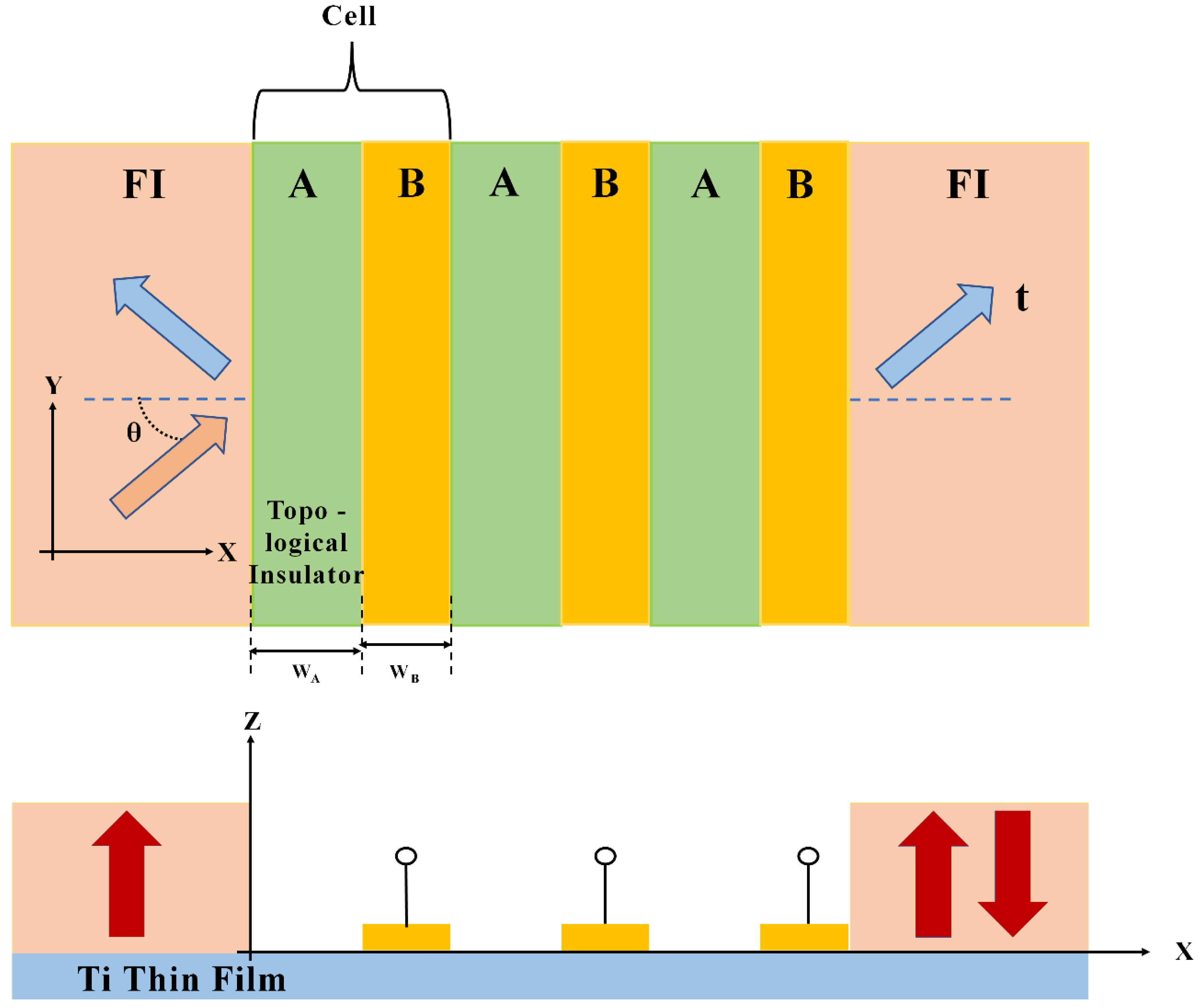
4.1. TIs as a Spintronics Device

TIs are a new class of materials that contain novel quantum states. Gapless Dirac surface states shielded by T-symmetry are created as a result of a nontrivial band topology and strong SOCs, and surface conductions display unusual spin-momentum locking properties, as shown in Figure 9 [93].
The 3D transition metal (TM) Mn is an uncommon magnetic doping agent that induces ferromagnetic order in chalcogenide TIs. It is frequently used as a dopant to add long-range ferromagnetic order to typical dilute magnetic semiconductors. The TRS-breaking effect in TIs was originally identified in Bi2Se3 doped with Mn [52]. Angle RESOLUTION PHOTOEMISSION SPECTROSCOPY (ARPES) has revealed a sizable Zeeman gap at the surface state (SS) Dirac cone [53,54], despite the fact that QAHE in Mn-doped TIs has never been noted. Research on the characteristics of Mn doped TIs is still in its infancy. There are currently many different dopants sites, magnetic transition temperatures, electronic states, saturation magnetizations, and anisotropies that can be seen in samples that are nominally identical in preparation. Mn dopants frequently enter TI hosts.

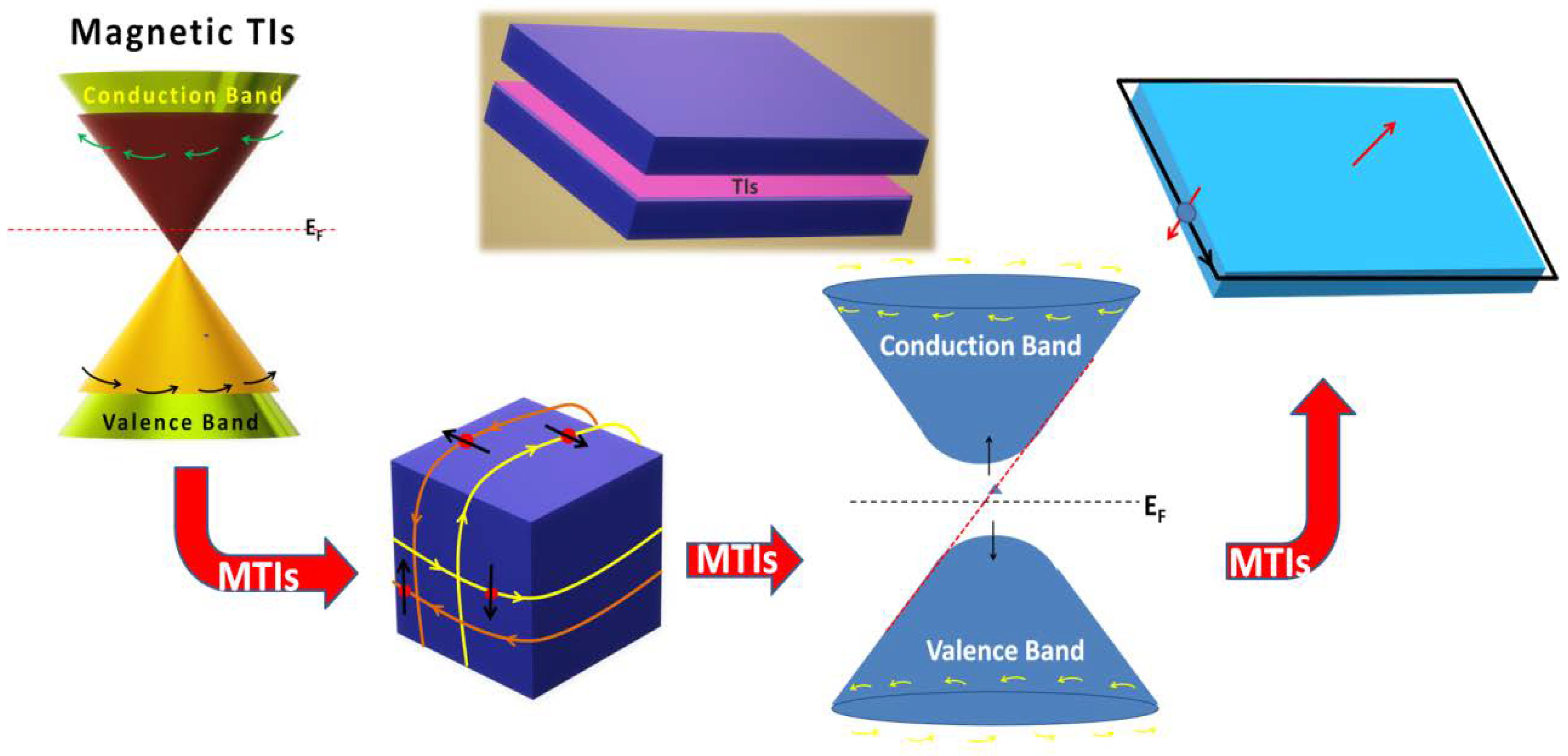
4.2. Magnetic Topological Insulator (MTIs)

The topology of the electronic wave-functions in combination with the magnetic spin configuration greatly affects the properties of a class of substances known as magnetic topological materials. These materials offer a wide range of applications, including dissipation-free spin and charge transport, information storage, and control. They can support chiral electronic channels with perfect conduction. Theoretical predictions of the QAHE without Landau levels and the most recent identification of magnetic Weyl semimetals and anti-ferromagnetic TIs are discussed in this article along with experimental developments in the study of magnetic topological materials. A number of experiments were performed to produce Chern insulators, indicating Weyl and Dirac magnetic semimetals having axionic and higher-order topological phases of matter.

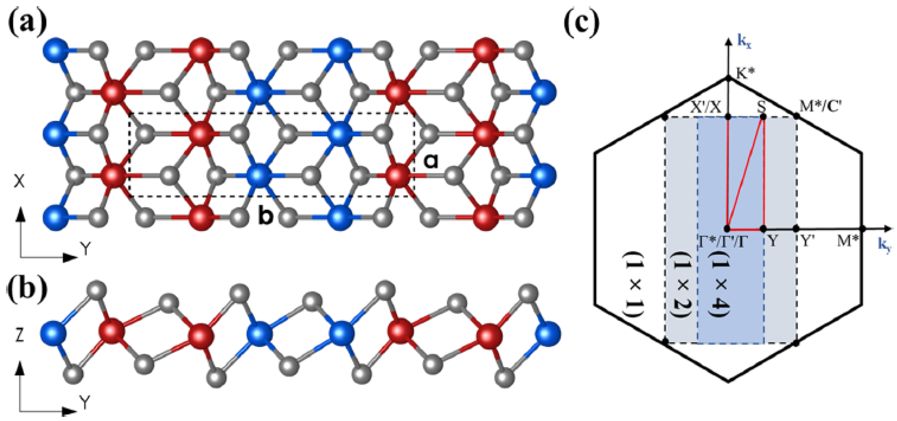
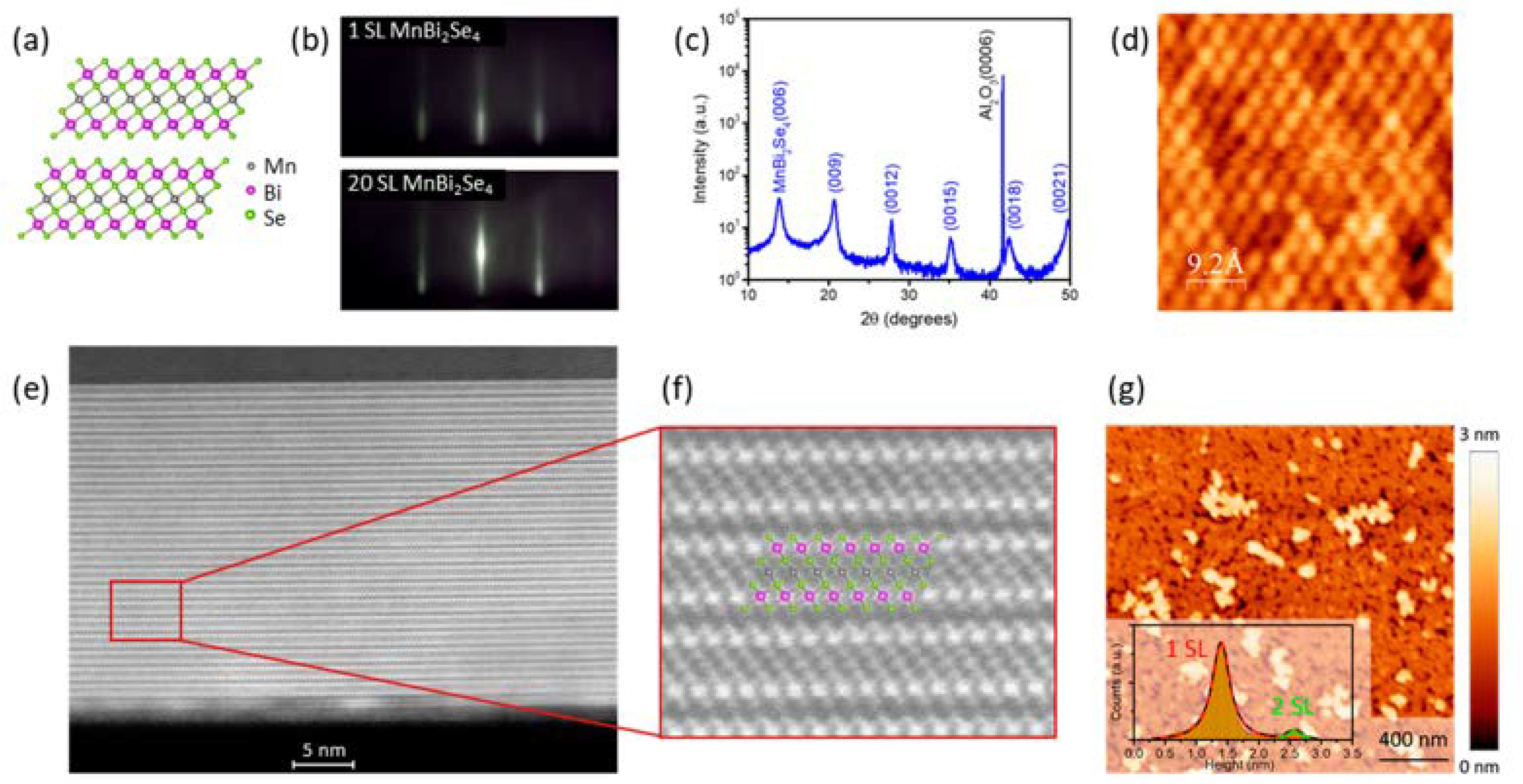
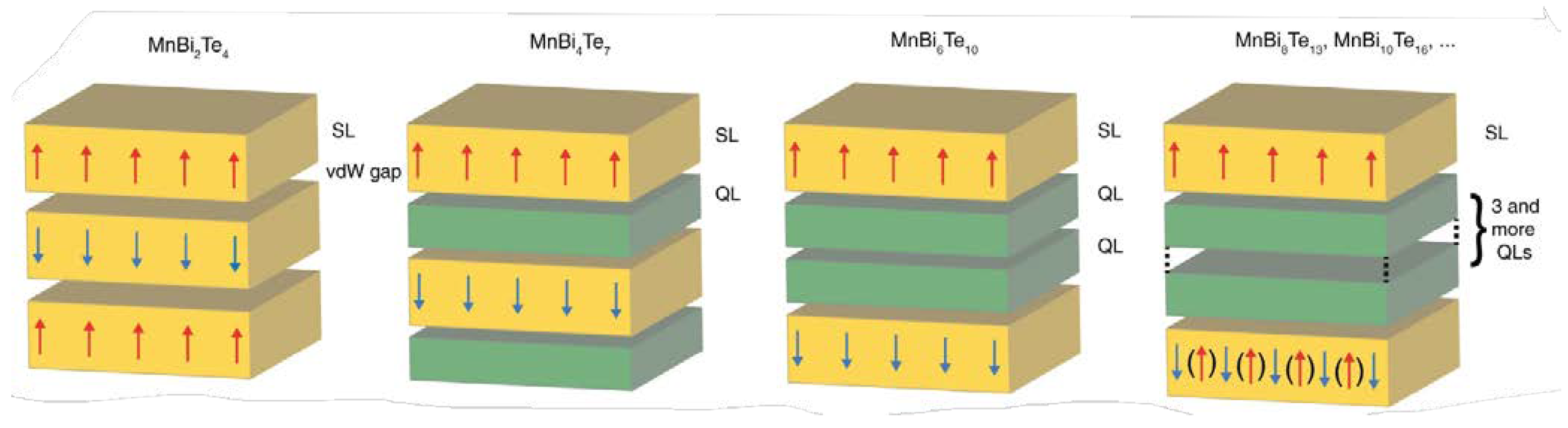
4.3. MnBi2Te4 a Classical Topological Insulator

The intrinsic MTIs MnBi2Te4 has attracted much attention due to its special magnetic and topological properties (Figure 10). To date, most reports have focused on bulk or flake samples. For material integration and device applications the epitaxial growth of MnBi2Te4 film in nanoscale is more important but challenging. Here, we report the growth of self-regulated MnBi2Te4 films by the MBE. By tuning the substrate temperature to the optimal temperature for the growth surface, the stoichiometry of MnBi2Te4 becomes sensitive to the Mn/Bi flux ratio. A MnTe phase and a Bi2Te3 phase respectively were formed in response to excess and insufficient Mn.
Superconducting quantum interference device (SQUID) magnetic studies of a 7 SLs MnBi2Te4 film shows that antiferromagnetic order and an anomalous magnetic hysteresis loop along the c-axis coexist at the Néel temperature of 22 K. Band structure investigations using angle-resolved photoemission spectroscopy (ARPES) at 80 K reveal a Dirac-like surface state, indicating that the paramagnetic phase of MnBi2Te4 has topological insulator characteristics.
Earlier discussion lays out the crucial growth parameters for the design and optimization of the synthesis of nanoscale MnBi2Te4 films which are essential for basic science and device applications requiring antiferromagnetic TIs. MBE is the most sophisticated way to fabricate van der Waals (vdW) materials like MnBi2Te4 [95,96]. Additionally, the thin-film arrangement can serve as an appropriate platform to realize several artificial MnBi2Te4 stacking structures, such as heterostructures and hybrid systems with other materials as ferromagnets [97,98].

4.4. Optimistic Approach towards Topological Insulator Antiferromagnetic in Spintronic

The new time-reversal symmetry-breaking physics can be realized using MTIs from the tetradymite family and related ternary compounds by exploiting the special Néel order in an antiferromagnet CrSb and the topological order in a magnetic topological insulator Cr-doped (Bi,Sb)2Te3 produced by MBE. Various heterostructures are proved to be successful at manipulating these diverse quantum states. It has been demonstrated that artificial structural engineering can be used to specifically shape emergent interfacial magnetic interactions. Exchange coupling at interfaces and exchange coupling between antiferromagnets were found to have an impact on the topological magnetism as mediated by the massive Dirac fermions by examining bilayers, tri layers, and superlattices consisting of these two components. Through measurements of magneto-electrical transport polarized neutron reflectometry/diffraction, the manipulation of the mass of Dirac fermions by using various Cr doping concentrations and the relationship between the magnetic spin textures of the antiferromagnet of the magnetic TIs was further investigated. These investigations demonstrate the antiferromagnet’s effectiveness as a layer for the massive Dirac fermions of the magnetic TIs interfacial and interlayer exchange coupling which also results in a significant improvement in magnetic ordering. A new foundation for topological antiferromagnetic spintronics is provided by this work. In condensed matter physics, the QAHE is a crucial quantum transport phenomenon. Since the QAHE has only ever been experimentally produced for Cr/V-doped (Bi, Sb)2Te3 at a very low observational temperature, its potential use in dissipation less quantum electronics has been severely constrained.

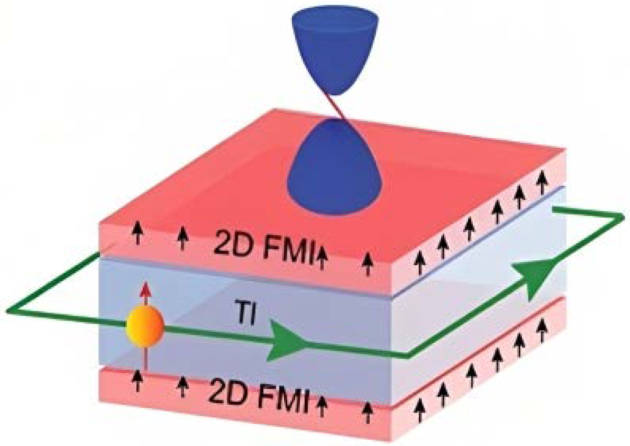
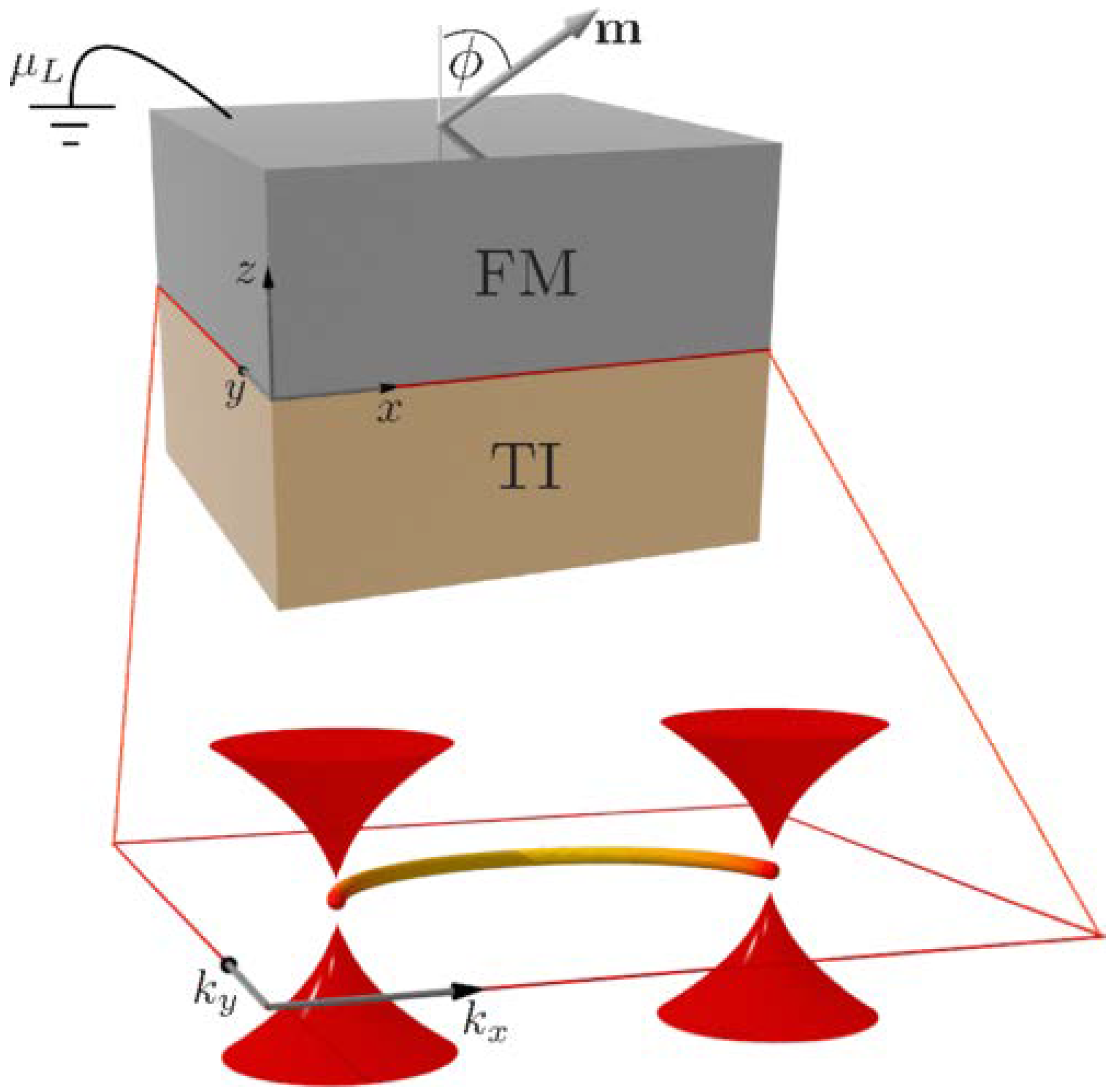
4.5. MTIs Spintronics Application

A new technique called spintronics, also known as magneto-electronics or spin transport electronics, makes use of the electron’s magnetic moment and intrinsic spin in addition to its fundamental electrical charge. A robust approach is used to develop MTIs for spintronic devices. The two most important physics problems in semiconductors and metals are spin transport and spin relaxation. A novel technology is being used in electronic storage technology that uses various spin parity phenomena such as MTIs, TIs, and GMR. The giant-magneto resistance (GMR) a sandwich structure which is made up of alternating ferromagnetic and non-magnetic metal layers was developed using spintronics. The device resistance varies from small (parallel magnetizations) to large (perpendicular magnetizations). Antiparallel magnetizations depend on the relative direction of the magnetizations in the magnetic layers (Figure 11) [99]. Magnetic field differences are detected using this variation in resistance also known as magneto resistance (MR). One of two possible positions for an electrons magnetic field is up or down as a result two additional binary states are added to the standard high and low logic values represented by current. These four states are a representation of quantum bits or qubits. Spintronic technology is used in mass storage devices. It is employed to cram a large amount of data into a small amount of space. It is also used in the medical industry for cancer detection. Digital electronics can benefit from spintronic technology in general. Mass storage hard drives have undergone testing.
Spintronics has been hailed as a viable low power alternative to current silicon-based transistors. These transistors switching process produces heat and this issue ends up in performance failure. A spintronics device relies on electron spin rather than electricity. An electron’s spin and mobility are correlated in a topological insulator, indicating that if a device can control electrons route, it can also control its spin. This suggests that “up” or “down” spin states might be controlled like bits in a computer. Theoretically, such a device would maintain its coolness. In light of the aforementioned behavior, researchers from Pennsylvania State University and the University of Chicago showed how to “draw” circuits on a topological insulator using visible or UV light [100]. The scientists compared their method to a “quantum Etch-a-Sketch” since the circuits stayed in place for several hours. The amazing characteristics of this sort of spintronics computing system such as low power dissipation, quantum computing and ultra-high computing speed make it a great replacement for conventional systems. The scientists compared their method to a “quantum Etch-a-Sketch” since the circuits stayed in place for several hours.
A report on enormous MR in TIs spin-valves at room temperature was published in 2021 by Peng Tseng et al. [101]. To increase the MR value a TIs thin film spin-valve with a segment gate-controlled potential is suggested. In contrast to conventional bulk TIs, a thin film of TIs, such as BiSbTeSe2, is utilized in the spin valve in this study. The findings point to a high band-structure-adopting MR value at room temperature of more than 1000%. In the antiparallel form, the current is severely constrained, whereas the parallel configuration displays a high chance of spin electron transmission. With regard to the spin transport behavior to cutting-edge spin-valve devices, the feature is significantly tunable. Figure 12 illustrates the suggested structure.
Future spintronics projects the optical or magnetic injection to produce spin-polarized interfaces between semiconductors and superconductors for transport Spin relaxation in semiconductors, metals amplifiers, and PN junctions. In the past few years spintronics exploiting MTIs SOCs nanomaterials has rapidly advanced. When a charge current is run through TIs, they display exceptionally strong SOCs and nontrivial topological surface states that develop in the bulk band topology order which distinguishes them from typical heavy metals and allows them to be used to efficiently alter neighboring magnetic materials. The most current advancements in the field of magnetic spintronics based on TIs are covered in this article. Our main areas of interest are the spin orbit torque induced magnetization switching in magnetic TIs structures, effects of spin injection and spin pumping in TIs magnet systems as well as electrical detection of the surface spin-polarized current in TIs.
A lot of the study of TIs has not progressed beyond the theoretical level. There has been a flood of reports on publications that investigate TIs inherent features. They focus mostly on QSH and superconductivity calculations as well as the TIs surface state and first-principle calculations of these phenomena. However, there is not nearly as much research on the application of TIs. Hence, many such implementations fall short of expectations. This is because TIs-based devices practical performance falls short of their theoretical maximum. The TIs have many notable qualities such as optical, electrical and magnetic properties. TIs have a wide variety of other potential applications. Better quality factor and less power consumption make TIs a prime candidate for application in batteries, gas sensors, solar cells and memories. TIs would make it possible to build the qubit computer, a new technology that would store and manipulate information by using the way atoms move. The dedicative advantages of TIs which set them apart from traditional semi electric allow them to be used in such ways that could lead to big changes in electronic devices in the future. Still, synthetic topological insulator nanostructures require a lot of work to figure out how to make electronic devices with new ideas and new ways of working.

4.6. Realizing Topological Superconductivity in Topological Insulator Materials

Numerous non crystalline materials have been used to create TIs with bulk-boundary correspondence, the most notable of which being amorphous networks, quasicrystals, and fractal lattices. As their nucleation occurs around a clearly defined Fermi surface with a Fermi momentum, their existence, which depends on the underlying translational symmetry and topological superconductors outside the realm of quantum crystals, remains untapped. Here, we describe a class of non-crystalline Dirac materials that lack translational symmetry and on which topological superconductors can be produced by proper local or on-site pairings. We present this result for all of the non-crystalline platforms stated above that are embedded in a two-dimensional flat space. The resulting non crystalline topological superconductors have a strong one-dimensional Majorana edge and a quantized topological invariant (Bott index). The majority of superconductors currently exist as s-wave superconductors with spin-singlet pairing and these traditional s-wave pristine superconductors display nontopological properties. According to our knowledge a Cooper pair’s total spin (S) can exist in one of two states [102]: either the spin-singlet pairing state with S = 0 or the spin-triplet pairing state with S = 1. In order to meet opposing parity of the total wave function odd parity of the wave function of a Cooper pair (S = 0) necessitates even parity of the orbital wave function (L = 0, 2, 4, ...). Additionally, s-wave or d-wave coupling is indicated by L = 0 or 2, respectively. The orbital wave function should be odd parity [L = 1 (p-wave), 3 (f-wave), 5, ...] in spin-triplet states (S = 1). Most superconductors including ordinary superconductors, cuprate superconductors, [103] and iron-based superconductors, are known to possess spin-singlet pairing states [104]. Therefore, although being fairly uncommon, TRS-breaking superconductors with spin-triplet pairing states have drawn a lot of attention in the quest for TSCs. “Intrinsic” TSCs are pristine superconductors with nontrivial topology and unusual pairing symmetry. There are only a few potential spin-triplet superconductors in existence. Several contenders may have spin-triplet pairing based on strong evidence, but none has been as conclusively shown as superfluid 3He. Sr2RuO4 and UPt3 are the attractive options for spin-triplet pairing despite having low superconducting transition temperatures (Tc). Other potential spin-triplet superconductors include noncentrosymmetric (lacking inversion symmetry) superconductors such as Li2Pt3B and ferromagnetic heavy fermion superconductors, such as UGe2 and UCoGe [105]. It is possible that the recently found quasi-1D-structured K2Cr3As3 family also has an unusual pairing state [106].

4.7. Doped Based Typical Topological Superconductor for Topological Insulator

By varying the carrier density/Fermi level or applying chemical pressure, chemical doping intercalation is frequently used to generate superconductivity in electron correlation systems to examine fascinating physics. Table 3 summarized the undoped TIs superconductor with their superconducting transition temperature, and space group.For instance, electron doping enabled the realization of superconductivity in fluorine-doped LaOFeAs, ushering in the era of iron-based superconductors [107]. Doping materials with lower radii such as P-for-As doping in BaFe2As2 can also cause chemical pressure [108]. The QAHE ferromagnetism in diluted magnetic semiconductors and diluted magnetic oxides represent two other amazing physical phenomena that have been found in magnetic element-doped systems [109]. As a result, doping or intercalating a TIs is a naturally intriguing method of investigating putative TSCs [110]. Table 4 gives a summary of the superconductivity generated by doping in TIs or TCIs. Tc is the superconducting transition temperature for various doping contents x.

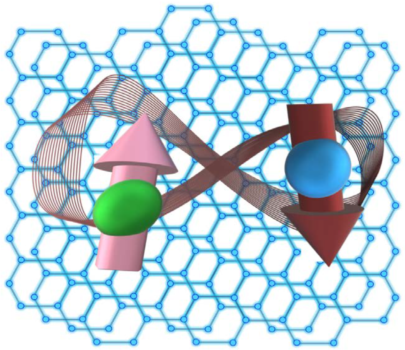
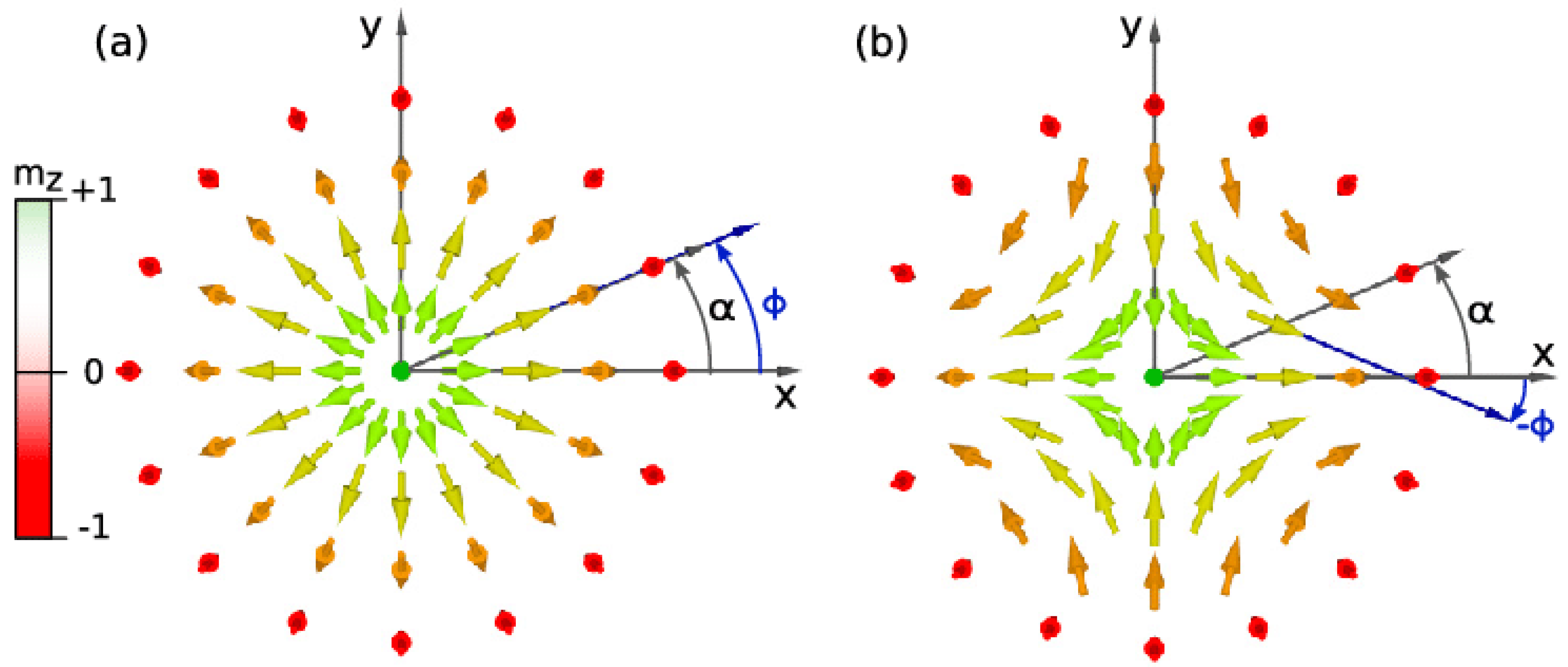
4.8. MTIs as a Potential Application in Magnetic Skyrmions Device

The structure of the magnetic skyrmion is defined by the spin whirling, vortex-like pattern, which means that all the constituent spin moments in the two-dimensional sheet only wrap the sphere once. Due to the driven motion with low electric-current excitation, topological protection and magnetic skyrmion’s nature spintronics may one day benefit from this extraordinary metastability. The skyrmions frequently manifest themselves in the form of crystal lattices such as hexagonal lattices in magnetic materials, but they can also occasionally appear as isolated or independent particles.
The texture of the magnetization contains tiny swirling topological defects called magnetic skyrmions, listed Table 5. Their topological characteristics have a significant impact on both their dynamics and stabilization. They are typically brought on by chiral interactions between atomic spins in thin films with broken inversion symmetry or non-centrosymmetric magnetic compounds (Figure 13).

4.9. Emerging Topological Insulators for Future Representatives

Owing to the availability of a broad pool of elements within the half-Heusler family, the physical characteristics of these materials may be modified by selecting the necessary element combination.
However, “it received much attention only in the 1980s with the discovery of the quantum Hall effect (QHE) [1]. In order to create the QHE electron, gas must be contained in two dimensions and subjected to extremely low temperatures and a strong magnetic field. As a result, its conductance is quantized and electrons start to flow at the materials edges without being stopped by dissipation-related phenomena. Fu et al. made the initial prediction of TIs 3D analogues of the metallic edge states [162]. In contrast to the requirements for the QHE in 3D TIs an external magnetic field is not required and is observed due to intrinsic SOC. After the discovery of TIs properties in Bi1−xSbx alloys, there was a surge in the discovery of other similar 3D materials, which demonstrated the TIs phenomenon [163]. Half-Heusler compounds (HHC) are the latest addition to the TIs family (Table 6). The half-Heusler compounds are non-centrosymmetric interpenetrating fcc crystal structures, lacking inversion symmetry, and are known for their multidisciplinary applications. HHC are composed of three elements (XYZ) with the rare earth based half-Heusler compounds being of significant interest to the condensed matter community owing to their various properties such as superconductivity [164] heavy fermion and Kondo behavior [165] and hosting various magnetic ground state effects. The desired properties of these half-Heusler can be tuned via various permutations and combination of the elements to facilitate SOC (with specific combinations of rare-earth elements and main-group elements) and by varying the hybridization (by the application of pressure) [166]. The 18-valence electron HHC are natural semimetals and ideal candidate for studying topological phenomena. In contrast to the two-dimensional TIs, HgTe (can be considered as a defect variant of a typical HHC XYZ) many HHC show a bulk band gap which is a pre-requisite for observing TIs-related behavior. The experimental verification of TIs is conducted by Angle-resolved photoemission spectroscopy (ARPES) which was instrumental in identifying surface states of the TIs compounds such as Bi1−xSbx (x = 0.12–0.13) [167], Bi2Se3 [168] and Bi2Te3 [169]. Due to the single surface Dirac cone in Bi2Se3 it was chosen as the ideal 3D TIs candidate for crucial fundamental studies. In other such 3D TIs systems the surface Dirac cone exists just beneath the top of the valence band complicating the study of the surface transport properties. However due to the presence of nonmagnetic elements in the Bi–Sb system, the magnetic ground state is not present. Bi2Se3 was selected as the optimum 3D TIs candidate for critical basic studies due to its single surface Dirac cone. The investigation of the surface transport features is made more challenging in other similar 3D TIs systems where the surface Dirac cone is located just below the top of the valence band”. The magnetic “ground state is absent in the Bi-Sb system due to the presence of nonmagnetic components. HHC come to the rescue at this point because the presence of rare-earth elements makes it possible for the magnetic ground state and topological behavior to coexist. Type-II antiferromagnetic state expression is made possible by using the examples of YPtBi and GdPtBi where the Y atom lacks the f-electrons in its system while Gd contains the f-electrons [170]. However, it is difficult to predict the location of the Dirac point and the number of surface states crossing the fermi level, as is evident from the ARPES results of the tetradymite family (TlBiX2, X = Se, Te). This difference can be attributed to the strong spin orbit contribution from the Te as compared to the Se. The ARPES results on LuPtBi by Liu et al. [171] show the metallic surface electronic state while studies by other groups [172] on the same system confirms the topological surface states. The discrepancy in these reports might be due to the differences involved in their respective approaches to the cleaving plane for the purposes of their study and the presence of dangling bonds, as ARPES measurement on LuPtBi were conducted on the freshly cleaved surface along (111) direction in both the experiments. TIs can also be characterized indirectly through transport measurements, such as magneto-resistance and their analysis via Shubnikov-de-Hass (SdH) oscillations, determining the Berry phase factor. However, separation of surface states from the bulk states is difficult in transport measurement techniques when the surface bands lie inside the bulk of the valence band. The Hall measurement study helps in determining the transport mechanism and contributes to understanding the origin of SdH oscillations in the system. Calculation of the Berry phase factor can also be performed independently through Hall measurements” [173].

5. Major Challenges in TIs

There seems to be no doubt that the TIs will face significant challenges in the development of the MTIs, per the summary and analysis.
Controlling the electron spin can be achieved with a material called a topological insulator and it has major challenges because it behaves as an insulator on the inside but is highly conductive on the surface. So, keeping in view of these states manufacturing and implementing magnetic topological insulator-based material has been limited. It involves several quantum phenomena, e.g., scattering of electrons or scattering of conduction electron in a metal due to magnetic impurities whose resulting characteristics change in the resistivity with temperature in the magnetic topological insulator. Electrical transport measurements frequently do not provide clear access to purely magnetic topological surface states since vacancies and site defects are invariably present, as in the case of materials of the Bi2Te3 type [185]. Discovering more topological insulator over 50 materials have not been experimentally tested which is great task to develop magnetic topological insulator with Majorma fermions, Dirac type massive fermions and Wiley type massless fermions based magnetic material for magnetic topological insulator. This is a challenge because when combining with a superconductor type material, its states create mismatch.
When magnetic topological insulator is applied in photonic device control becomes very difficult. There are technical hurdles to overcome in downsizing the system and in another hand a photonic analogue of magnetic based TIs was latest predicted on the basis of the anticipated arrangement of permittivity and permeability matched bianisotropic material in 2Ds super lattice. Observation of a magnetic topological insulator for photonic devices is challenging because bianisotropic metamaterial is usually highly dispersive. Recent measurements have also shown that the surface-transport properties in MTIs have ageing effects. These problems offer both a significant challenge and an excellent chance for surface chemical changes. Growing a protective layer over newly exposed surfaces for MTIs could be challenging.
Due to the special properties of magnetic TIs controlling the edge state will be a ground-breaking effort in the advancement of MTIs. Uncompensated magnetic moment and localized spin canting may occur in the case of AFM material. However, this effect is typically localized and disordered which hardly affects the magnetic TIs general properties. The impact of heat temperature on MTIs which lowers device efficiency is yet another extremely important problem. TIs are thus considered with optimism as mass-Dirac particles, which are crucial in low-dissipation circuits, are less common. This opens the door for the creation of energy-efficient technology. In reference to topological suppression from bulk states consequences the dynamical, electrical and magnetic characteristics of TIs surface state must also be investigated by researchers using the Dirac electron. This must boost TIs development and have an impact on scholars everywhere.

6. Conclusions and Future Prospects

TIs will witness increased practical use in the future particularly in various fields, e.g., condensed states physics, macro-microelectronic, and communication technology. Because of the fascinating metallic states and the surface inherent Dirac point without spin, degeneracy will result in the production of particles useful for quantum computing. Metallic surfaces are possible candidates for novel spintronic devices. Majorana spin half particles which can be produced at the boundary between a TIs and a superconductor are also just one step away from a topological quantum computer that is error-proof. The controllability of TIs interaction with magnetic material currently prevents their incorporation into spintronic devices and quantum computing systems. Although surface state machinations and heterogeneous amalgamation have only been partially realized thus far, it is anticipated that future work on methods of synthesis and device optimization will lead to the development of a variety of novel nanoelectronics, optoelectronics, and spintronics applications.

Author Contributions

Conceptualization—P.K., R.K. (Ravi Kumar), V.K. and A.G.; Methodology—M.K.K., R.K. (Ravinder Kumar), A.G. and V.K.; Software—P.K., R.K. (Ravi Kumar), S.K. and V.K.; Resources—P.K., R.K. (Ravi Kumar) and S.K.; Writing—Original Draft—P.K., R.K. (Ravi Kumar) and S.K.; Writing—Review & Editing—M.K.K., R.K. (Ravinder Kumar), V.K. and A.G.; Supervision—A.G. and V.K. All authors have read and agreed to the published version of the manuscript.

Funding

This research received no external funding.

Conflicts of Interest

The authors declare no conflict of interest.

References

  1. Klitzing, K.V.; Dorda, G.; Pepper, M. New Method for High-Accuracy Determination of the Fine-Structure Constant Based on Quantized Hall Resistance. Phys. Rev. Lett. 1980, 45, 494. [Google Scholar] [CrossRef] [Green Version]
  2. Maciejko, J.; Hughes, T.L.; Zhang, S.-C. The Quantum Spin Hall Effect. Annu. Rev. Condens. Matter Phys. 2011, 2, 31–53. [Google Scholar] [CrossRef]
  3. Qi, X.-L.; Zhang, S.-C. The quantum spin Hall effect and topological insulators. Phys. Today 2010, 63, 33–38. [Google Scholar] [CrossRef] [Green Version]
  4. Moore, J. Topological insulators: The next generation. Nat. Phys. 2009, 5, 378–380. [Google Scholar] [CrossRef]
  5. Wang, B.; Zhong, S.; Xu, P.; Zhang, H. Recent development and advances in Photodetectors based on two-dimensional topological insulators. J. Mater. Chem. C 2020, 8, 15526–15574. [Google Scholar] [CrossRef]
  6. Zunger, A.; Malyi, O.I. Understanding Doping of Quantum Materials. Chem. Rev. 2021, 121, 3031–3060. [Google Scholar] [CrossRef]
  7. Yang, M.; Zhou, H.; Wang, J. Topological insulators photodetectors: Preparation, advances and application challenges. Mater. Today Commun. 2022, 33, 104190. [Google Scholar] [CrossRef]
  8. Köenig, M.; Wiedmann, S.; Brüene, C.; Roth, A.; Buhmann, H.; Molenkamp, L.W.; Qi, X.-L.; Zhang, S.-C. Quantum Spin Hall Insulator State in HgTe Quantum Wells. Science 2007, 318, 766–770. [Google Scholar] [CrossRef] [Green Version]
  9. Bernevig, B.A.; Hughes, T.L.; Zhang, S.-C. Quantum Spin Hall Effect and Topological Phase Transition in HgTe Quantum Wells. Science 2006, 314, 1757–1761. [Google Scholar] [CrossRef] [Green Version]
  10. Luo, J.-W.; Zunger, A. Design Principles and Coupling Mechanisms in the 2D Quantum Well Topological Insulator HgTe/CdTe. Phys. Rev. Lett. 2010, 105, 176805. [Google Scholar] [CrossRef] [Green Version]
  11. Knez, I.; Du, R.-R.; Sullivan, G. Evidence for Helical Edge Modes in Inverted InAs/GaSb Quantum Wells. Phys. Rev. Lett. 2011, 107, 136603. [Google Scholar] [CrossRef] [Green Version]
  12. Knez, I.; Du, R.-R.; Sullivan, G. Andreev Reflection of Helical Edge Modes in InAs/GaSb Quantum Spin Hall Insulator. Phys. Rev. Lett. 2012, 109, 186603. [Google Scholar] [CrossRef] [Green Version]
  13. Xu, H.; Han, D.; Bao, Y.; Cheng, F.; Ding, Z.; Tan, S.J.R.; Loh, K.P. Observation of Gap Opening in 1T′ Phase MoS2 Nanocrystals. Nano Lett. 2018, 18, 5085–5090. [Google Scholar] [CrossRef]
  14. Liu, L.; Guo, J. Assessment of performance potential of MoS2-based topological insulator field-effect transistors. J. Appl. Phys. 2015, 118, 124502. [Google Scholar] [CrossRef]
  15. Sankar, R.; Rao, G.N.; Muthuselvam, I.P.; Butler, C.; Kumar, N.; Murugan, G.S.; Shekhar, C.; Chang, T.-R.; Wen, C.-Y.; Chen, C.-W.; et al. Polymorphic Layered MoTe2 from Semiconductor, Topological Insulator, to Weyl Semimetal. Chem. Mater. 2017, 29, 699–707. [Google Scholar] [CrossRef]
  16. Gan, Y.; Liang, J.; Cho, C.-W.; Li, S.; Guo, Y.; Ma, X.; Wu, X.; Wen, J.; Du, X.; He, M.; et al. Bandgap opening in MoTe2 thin flakes induced by surface oxidation. Front. Phys. 2020, 15, 33602. [Google Scholar] [CrossRef]
  17. Zhou, X.; Jiang, Z.; Zhang, K.; Yao, W.; Yan, M.; Zhang, H.; Duan, W.; Zhou, S. Electronic structure of molecular beam epitaxy grown 1 T ′ -MoTe2 film and strain effect. Chin. Phys. B 2019, 28, 107307. [Google Scholar] [CrossRef] [Green Version]
  18. Liu, S.; Wang, M.X.; Chen, C.; Xu, X.; Jiang, J.; Yang, L.X.; Yang, H.F.; Lv, Y.Y.; Zhou, J.; Chen, Y.B. Experimental Ob-servation of Conductive Edge States in Weak Topological Insulator Candidate HfTe5. APL Mater. 2018, 6, 121111. [Google Scholar] [CrossRef] [Green Version]
  19. Chang, C.; Chen, W.; Chen, Y.; Chen, Y.; Chen, Y.; Ding, F.; Fan, C.; Fan, H.J.; Fan, Z.; Gong, C.; et al. Recent Progress on Two-Dimensional Materials. Acta Phys. Chim. Sin. 2021, 37, 2108017. [Google Scholar] [CrossRef]
  20. Empante, T.A.; Zhou, Y.; Klee, V.; Nguyen, A.E.; Lu, I.-H.; Valentin, M.D.; Naghibi Alvillar, S.A.; Preciado, E.; Berges, A.J.; Merida, C.S. Chemical Vapor Deposition Growth of Few-Layer MoTe2 in the 2H, 1T′, and 1T Phases: Tunable Properties of MoTe2 Films. ACS Nano 2017, 11, 900–905. [Google Scholar] [CrossRef]
  21. Di, J.; Xia, J.; Li, H.; Liu, Z. Freestanding atomically-thin two-dimensional materials beyond graphene meeting photocatalysis: Opportunities and challenges. Nano Energy 2017, 35, 79–91. [Google Scholar] [CrossRef]
  22. Liu, R.-Z.; Huang, X.; Zhao, L.-X.; Liu, L.-M.; Yin, J.-X.; Wu, R.; Chen, G.-F.; Wang, Z.-Q.; Pan, S.H. Experimental Observations Indicating the Topological Nature of the Edge States on HfTe5. Chin. Phys. Lett. 2019, 36, 117301. [Google Scholar] [CrossRef] [Green Version]
  23. Zhang, Y.; Wang, C.; Liu, G.; Liang, A.; Zhao, L.; Huang, J.; Gao, Q.; Shen, B.; Liu, J.; Hu, C.; et al. Temperature-induced Lifshitz transition in topological insulator candidate HfTe 5. Sci. Bull. 2017, 62, 950–956. [Google Scholar] [CrossRef] [Green Version]
  24. Li, H.; Liu, S.; Liu, C.; Zhang, J.; Xu, Y.; Yu, R.; Wu, Y.; Zhang, Y.; Fan, S. Antiferromagnetic topological insulator MnBi2Te4: Synthesis and magnetic properties. Phys. Chem. Chem. Phys. 2019, 22, 556–563. [Google Scholar] [CrossRef] [Green Version]
  25. Deng, Y.; Yu, Y.; Shi, M.Z.; Guo, Z.; Xu, Z.; Wang, J.; Chen, X.H.; Zhang, Y. Quantum Anomalous Hall Effect in Intrinsic Magnetic Topological Insulator MnBi2Te4. Science 2020, 367, 895–900. [Google Scholar] [CrossRef] [Green Version]
  26. Asaba, T.; Wang, Y.; Li, G.; Xiang, Z.; Tinsman, C.; Chen, L.; Zhou, S.; Zhao, S.; Laleyan, D.; Li, Y.; et al. Magnetic Field Enhanced Superconductivity in Epitaxial Thin Film WTe2. Sci. Rep. 2018, 8, 6520. [Google Scholar] [CrossRef]
  27. Zhao, C.; Hu, M.; Qin, J.; Xia, B.; Liu, C.; Wang, S.; Guan, D.; Li, Y.; Zheng, H.; Liu, J. Strain Tunable Semimetal–Topological-Insulator Transition in Monolayer 1 T′− WTe 2. Phys. Rev. Lett. 2020, 125, 046801. [Google Scholar] [CrossRef]
  28. Shahil, K.M.F.; Hossain, M.Z.; Goyal, V.; Balandin, A.A. Micro-Raman Spectroscopy of Mechanically Exfoliated Few-Quintuple Layers of Bi2Te3, Bi2Se3, and Sb2Te3 Materials. J. Appl. Phys. 2012, 111, 054305. [Google Scholar] [CrossRef] [Green Version]
  29. Hong, S.S.; Kundhikanjana, W.; Cha, J.J.; Lai, K.; Kong, D.; Meister, S.; Kelly, M.A.; Shen, Z.X.; Cui, Y. Ultrathin Top-ological Insulator Bi2Se3 Nanoribbons Exfoliated by Atomic Force Microscopy. Nano Lett. 2010, 10, 3118–3122. [Google Scholar] [CrossRef] [Green Version]
  30. Shang, J.; Feng, T.; Zhao, S.; Li, T.; Pan, Z.; Zhao, J. Saturable Absorption Characteristics of Bi2Se3 in a 2 Μm Q-Switching Bulk Laser. Opt. Express 2020, 28, 5639–5647. [Google Scholar] [CrossRef]
  31. Sun, L.; Lin, Z.; Peng, J.; Weng, J.; Huang, Y.; Luo, Z. Preparation of Few-Layer Bismuth Selenide by Liq-uid-Phase-Exfoliation and Its Optical Absorption Properties. Sci. Rep. 2014, 4, 4794. [Google Scholar] [CrossRef] [Green Version]
  32. Bansal, N.; Cho, M.R.; Brahlek, M.; Koirala, N.; Horibe, Y.; Chen, J.; Wu, W.; Park, Y.D.; Oh, S. Transferring MBE-Grown Topological Insulator Films to Arbitrary Substrates and Metal–Insulator Transition via Dirac Gap. Nano Lett. 2014, 14, 1343–1348. [Google Scholar] [CrossRef] [Green Version]
  33. Schreyeck, S.; Tarakina, N.V.; Karczewski, G.; Schumacher, C.; Borzenko, T.; Brüne, C.; Buhmann, H.; Gould, C.; Brunner, K.; Molenkamp, L.W. Molecular Beam Epitaxy of High Structural Quality Bi2Se3 on Lattice Matched InP (111) Sub-strates. Appl. Phys. Lett. 2013, 102, 041914. [Google Scholar] [CrossRef] [Green Version]
  34. Yang, L.; Wang, Z.; Li, M.; Gao, X.P.A.; Zhang, Z. The Dimensional Crossover of Quantum Transport Properties in Few-Layered Bi2Se3 Thin Films. Nanoscale Adv. 2019, 1, 2303–2310. [Google Scholar] [CrossRef] [Green Version]
  35. Lee, Y.F.; Punugupati, S.; Wu, F.; Jin, Z.; Narayan, J.; Schwartz, J. Evidence for topological surface states in epitaxial Bi2Se3 thin film grown by pulsed laser deposition through magneto-transport measurements. Curr. Opin. Solid State Mater. Sci. 2014, 18, 279–285. [Google Scholar] [CrossRef]
  36. Kong, D.; Dang, W.; Cha, J.J.; Li, H.; Meister, S.; Peng, H.; Liu, Z.; Cui, Y. Few-Layer Nanoplates of Bi2Se3 and Bi2Te3 with Highly Tunable Chemical Potential. Nano Lett. 2010, 10, 2245–2250. [Google Scholar] [CrossRef] [Green Version]
  37. Alegria, L.D.; Schroer, M.D.; Chatterjee, A.; Poirier, G.R.; Pretko, M.; Patel, S.K.; Petta, J.R. Structural and Electrical Characterization of Bi2Se3 Nanostructures Grown by Metal-Organic Chemical Vapor Deposition. Nano Lett. 2012, 12, 4711–4714. [Google Scholar] [CrossRef] [Green Version]
  38. Li, H.; Wang, H.-W.; Li, Y.; Zhang, H.; Zhang, S.; Pan, X.-C.; Jia, B.; Song, F.; Wang, J. Quantitative Analysis of Weak Antilocalization Effect of Topological Surface States in Topological Insulator BiSbTeSe2. Nano Lett. 2019, 19, 2450–2455. [Google Scholar] [CrossRef]
  39. Sotor, J.; Sobon, G.; Macherzynski, W.; Paletko, P.; Grodecki, K.; Abramski, K.M. Mode-locking in Er-doped fiber laser based on mechanically exfoliated Sb2Te3 saturable absorber. Opt. Mater. Express 2013, 4, 1–6. [Google Scholar] [CrossRef]
  40. Al-Dabagh, Z.A.I.; Al-Masoodi, A.H.H.; Ahmed, M.H.M.; Latiff, A.A.; Harun, S.W. Q-Switched and Mode-Locked Er-bium-Doped Fiber Lasers Using Antimony Telluride (Sb2Te3) Saturable Absorbers. J. Nanoelectron. Optoelectron. 2019, 14, 1088–1094. [Google Scholar] [CrossRef]
  41. Orujlu, E.N.; Aliev, Z.S.; Amiraslanov, I.R.; Babanly, M.B. Phase Equilibria of the MnTe-Sb2Te3 System and Synthesis of Novel Ternary Layered Compound–MnSb4Te7. Phys. Chem. Solid State 2021, 22, 39–44. [Google Scholar] [CrossRef]
  42. Lewin, M.; Mester, L.; Saltzmann, T.; Chong, S.-J.; Kaminski, M.; Hauer, B.; Pohlmann, M.; Mio, A.M.; Wirtssohn, M.; Jost, P.; et al. Sb2Te3 Growth Study Reveals That Formation of Nanoscale Charge Carrier Domains Is an Intrinsic Feature Relevant for Electronic Applications. ACS Appl. Nano Mater. 2018, 1, 6834–6842. [Google Scholar] [CrossRef]
  43. Zeng, Z.; Morgan, T.A.; Fan, D.; Li, C.; Hirono, Y.; Hu, X.; Zhao, Y.; Lee, J.S.; Wang, J.; Wang, Z.M. Molecular Beam Epitaxial Growth of Bi2Te3 and Sb2Te3 Topological Insulators on GaAs (111) Substrates: A Potential Route to Fabricate Topological Insulator Pn Junction. AIP Adv. 2013, 3, 072112. [Google Scholar] [CrossRef]
  44. Newbrook, D.W.; Richards, S.P.; Greenacre, V.K.; Hector, A.L.; Levason, W.; Reid, G.; de Groot, C.H.K.; Huang, R. Selective Chemical Vapor Deposition Approach for Sb2Te3 Thin Film Micro-Thermoelectric Generators. ACS Appl. Energy Mater. 2020, 3, 5840–5846. [Google Scholar] [CrossRef]
  45. Rimoldi, M.; Cecchini, R.; Wiemer, C.; Longo, E.; Cecchi, S.; Mantovan, R.; Longo, M. Effect of Substrates and Thermal Treatments on Metalorganic Chemical Vapor Deposition-Grown Sb2Te3 Thin Films. Cryst. Growth Des. 2021, 21, 5135–5144. [Google Scholar] [CrossRef]
  46. Lee, C.W.; Kim, G.H.; Kang, S.G.; Kang, M.-A.; An, K.-S.; Kim, H.; Lee, Y.K. Growth behavior of Bi2Te3and Sb2Te3thin films on graphene substrate grown by plasma-enhanced chemical vapor deposition. Phys. Status Solidi (RRL) Rapid Res. Lett. 2017, 11. [Google Scholar] [CrossRef]
  47. Harrison, S.E.; Li, S.; Huo, Y.; Zhou, B.; Chen, Y.L.; Harris, J.S. Two-Step Growth of High Quality Bi2Te3 Thin Films on Al2O3 (0001) by Molecular Beam Epitaxy. Appl. Phys. Lett. 2013, 102, 171906. [Google Scholar] [CrossRef]
  48. Avron, J.E.; Osadchy, D.; Seiler, R. A Topological Look at the Quantum Hall Effect. Phys. Today 2003, 56, 38–42. [Google Scholar] [CrossRef]
  49. Yao, Y.; Ye, F.; Qi, X.-L.; Zhang, S.-C.; Fang, Z. Spin-orbit gap of graphene: First-principles calculations. Phys. Rev. B 2007, 75, 041401. [Google Scholar] [CrossRef] [Green Version]
  50. Zhang, T.; Jiang, Y.; Song, Z.; Huang, H.; He, Y.; Fang, Z.; Weng, H.; Fang, C. Catalogue of topological electronic materials. Nature 2019, 566, 475–479. [Google Scholar] [CrossRef] [Green Version]
  51. Li, Q.; Trang, C.X.; Wu, W.; Hwang, J.; Cortie, D.; Medhekar, N.; Mo, S.; Yang, S.A.; Edmonds, M.T. Large Magnetic Gap in a Designer Ferromagnet–Topological Insulator–Ferromagnet Heterostructure. Adv. Mater. 2022, 34. [Google Scholar] [CrossRef]
  52. Maghirang, A.B.; Huang, Z.-Q.; Villaos, R.A.B.; Hsu, C.-H.; Feng, L.-Y.; Florido, E.; Lin, H.; Bansil, A.; Chuang, F.-C. Predicting two-dimensional topological phases in Janus materials by substitutional doping in transition metal dichalcogenide monolayers. Npj 2D Mater. Appl. 2019, 3, 35. [Google Scholar] [CrossRef] [Green Version]
  53. Sufyan, A.; Macam, G.; Hsu, C.-H.; Huang, Z.-Q.; Huang, S.-M.; Lin, H.; Chuang, F.-C. Theoretical prediction of topological insulators in two-dimensional ternary transition metal chalcogenides (MM′X4, M = Ta, Nb, or V; M′= Ir, Rh, or Co; X = Se or Te). Chin. J. Phys. 2021, 73, 95–102. [Google Scholar] [CrossRef]
  54. Dobardžić, E.; Dimitrijević, M.; Milovanović, M.V. Generalized Bloch theorem and topological characterization. Phys. Rev. B 2015, 91, 125424. [Google Scholar] [CrossRef] [Green Version]
  55. Lin, Y.-M.; Rabin, O.; Cronin, S.B.; Ying, J.Y.; Dresselhaus, M.S. Semimetal–Semiconductor Transition in Bi1 − xSbx Alloy Nanowires and Their Thermoelectric Properties. Appl. Phys. Lett. 2002, 81, 2403–2405. [Google Scholar] [CrossRef]
  56. Liu, J.; Hsieh, T.H.; Wei, P.; Duan, W.; Moodera, J.; Fu, L. Spin-filtered edge states with an electrically tunable gap in a two-dimensional topological crystalline insulator. Nat. Mater. 2013, 13, 178–183. [Google Scholar] [CrossRef] [Green Version]
  57. Bergholtz, E.J.; Budich, J.C. Non-Hermitian Weyl physics in topological insulator ferromagnet junctions. Phys. Rev. Res. 2019, 1, 012003. [Google Scholar] [CrossRef] [Green Version]
  58. Bernevig, B.A.; Felser, C.; Beidenkopf, H. Progress and prospects in magnetic topological materials. Nature 2022, 603, 41–51. [Google Scholar] [CrossRef]
  59. Tian, W.; Yu, W.; Shi, J.; Wang, Y. The Property, Preparation and Application of Topological Insulators: A Review. Materials 2017, 10, 814. [Google Scholar] [CrossRef] [Green Version]
  60. Wang, Y.; Ramaswamy, R.; Yang, H. FMR-related phenomena in spintronic devices. J. Phys. D Appl. Phys. 2018, 51, 273002. [Google Scholar] [CrossRef] [Green Version]
  61. Liu, X.; Smith, D.J.; Fan, J.; Zhang, Y.-H.; Cao, H.; Chen, Y.P.; Leiner, J.; Kirby, B.J.; Dobrowolska, M.; Furdyna, J.K. Structural Properties of Bi2Te3 and Bi2Se3 Topological Insulators Grown by Molecular Beam Epitaxy on GaAs (001) Substrates. Appl. Phys. Lett. 2011, 99, 171903. [Google Scholar] [CrossRef]
  62. Plucinski, L.; Mussler, G.; Krumrain, J.; Herdt, A.; Suga, S.; Grützmacher, D.; Schneider, C.M. Robust surface electronic properties of topological insulators: Bi2Te3 films grown by molecular beam epitaxy. Appl. Phys. Lett. 2011, 98, 222503. [Google Scholar] [CrossRef] [Green Version]
  63. Krumrain, J.; Mussler, G.; Borisova, S.; Stoica, T.; Plucinski, L.; Schneider, C.M.; Grützmacher, D. MBE Growth Opti-mization of Topological Insulator Bi2Te3 Films. J. Cryst. Growth 2011, 324, 115–118. [Google Scholar] [CrossRef]
  64. Cao, H.; Venkatasubramanian, R.; Liu, C.; Pierce, J.; Yang, H.; Zahid Hasan, M.; Wu, Y.; Chen, Y.P. Topological In-sulator Bi2Te3 Films Synthesized by Metal Organic Chemical Vapor Deposition. Appl. Phys. Lett. 2012, 101, 162104. [Google Scholar] [CrossRef] [Green Version]
  65. Brom, J.E.; Weiss, L.; Choudhury, T.H.; Redwing, J.M. Hybrid physical–chemical vapor deposition of Bi2Se3 films. J. Cryst. Growth 2016, 452, 230–234. [Google Scholar] [CrossRef] [Green Version]
  66. Ali, Z.; Cao, C.; Li, J.; Wang, Y.; Cao, T.; Tanveer, M.; Tahir, M.; Idrees, F.; Butt, F.K. Effect of synthesis technique on electrochemical performance of bismuth selenide. J. Power Sources 2013, 229, 216–222. [Google Scholar] [CrossRef]
  67. Fei, F.; Wei, Z.; Wang, Q.; Lu, P.; Wang, S.; Qin, Y.; Pan, D.; Zhao, B.; Wang, X.; Sun, J. Solvothermal Synthesis of Lateral Heterojunction Sb2Te3/Bi2Te3 Nanoplates. Nano Lett. 2015, 15, 5905–5911. [Google Scholar] [CrossRef]
  68. Alegria, L.D.; Petta, J.R. Controlled MOCVD Growth of Bi2Se3 Topological Insulator Nanoribbons. Nanotechnology 2012, 23, 435601. [Google Scholar] [CrossRef] [Green Version]
  69. Bendt, G.; Zastrow, S.; Nielsch, K.; Mandal, P.S.; Sánchez-Barriga, J.; Rader, O.; Schulz, S. Deposition of topological insulator Sb2Te3 films by an MOCVD process. J. Mater. Chem. A 2014, 2, 8215–8222. [Google Scholar] [CrossRef] [Green Version]
  70. Lee, J.H.; Shin, D.W.; Makotchenko, V.G.; Nazarov, A.S.; Fedorov, V.E.; Kim, Y.H.; Choi, J.-Y.; Kim, J.M.; Yoo, J.-B. Expanded Graphite: One-Step Exfoliation Synthesis of Easily Soluble Graphite and Transparent Conducting Graphene. Adv. Mater. 2009, 21, 4383–4387. [Google Scholar] [CrossRef]
  71. Ambrosi, A.; Sofer, Z.; Luxa, J.; Pumera, M. Exfoliation of Layered Topological Insulators Bi2Se3 and Bi2Te3 via Electrochemistry. ACS Nano 2016, 10, 11442–11448. [Google Scholar] [CrossRef]
  72. Ren, L.; Qi, X.; Liu, Y.; Hao, G.; Huang, Z.; Zou, X.; Yang, L.; Li, J.; Zhong, J. Large-scale production of ultrathin topological insulator bismuth telluride nanosheets by a hydrothermal intercalation and exfoliation route. J. Mater. Chem. 2012, 22, 4921–4926. [Google Scholar] [CrossRef]
  73. Liu, H.; Li, Q.; Zhu, Y.; Zhang, M.; Liu, R.; Li, X.; Kang, X.; Li, Z.; Qiao, S. Synthesis and mechanical exfoliation of imine-linked two-dimensional conjugated polymers. J. Mater. Chem. C 2017, 6, 722–725. [Google Scholar] [CrossRef]
  74. Zhao, S.Y.F.; Beekman, C.; Sandilands, L.J.; Bashucky, J.E.J.; Kwok, D.; Lee, N.; LaForge, A.D.; Cheong, S.W.; Burch, K.S. Fabrication and characterization of topological insulator Bi2Se3 nanocrystals. Appl. Phys. Lett. 2011, 98, 141911. [Google Scholar] [CrossRef] [Green Version]
  75. Goyal, V.; Teweldebrhan, D.; Balandin, A.A. Mechanically-exfoliated stacks of thin films of Bi2Te3 topological insulators with enhanced thermoelectric performance. Appl. Phys. Lett. 2010, 97, 133117. [Google Scholar] [CrossRef] [Green Version]
  76. Zhang, X.; Li, Y.; Mu, W.; Bai, W.; Sun, X.; Zhao, M.; Zhang, Z.; Shan, F.; Yang, Z. Advanced tape-exfoliated method for preparing large-area 2D monolayers: A review. 2D Mater. 2021, 8, 032002. [Google Scholar] [CrossRef]
  77. Yan, P.; Lin, R.; Ruan, S.; Liu, A.; Chen, H.; Zheng, Y.; Chen, S.; Guo, C.; Hu, J. A practical topological insulator saturable absorber for mode-locked fiber laser. Sci. Rep. 2015, 5, srep08690. [Google Scholar] [CrossRef] [Green Version]
  78. Zareapour, P.; Hayat, A.; Zhao, S.Y.F.; Kreshchuk, M.; Jain, A.; Kwok, D.C.; Lee, N.; Cheong, S.-W.; Xu, Z.; Yang, A.; et al. Proximity-induced high-temperature superconductivity in the topological insulators Bi2Se3 and Bi2Te3. Nat. Commun. 2012, 3, 1056. [Google Scholar] [CrossRef] [Green Version]
  79. Nicolosi, V.; Chhowalla, M.; Kanatzidis, M.G.; Strano, M.S.; Coleman, J.N. Liquid Exfoliation of Layered Materials. Science 2013, 340, 1226419. [Google Scholar] [CrossRef] [Green Version]
  80. Wang, S.; Li, L.; Song, Y.-F.; Tang, D.-Y.; Shen, D.-Y.; Zhao, L.-M. Vector soliton and noise-like pulse generation using a Ti3C2 MXene material in a fiber laser. Front. Inf. Technol. Electron. Eng. 2020, 22, 318–324. [Google Scholar] [CrossRef]
  81. Yan, B.; Guo, H.; He, G.; Mao, J.; Wang, F.; Yang, K.; Zhang, B.; He, J. Ta2NiSe5 nanosheets as a novel broadband saturable absorber for solid-state pulse laser generation. Sci. China Mater. 2021, 64, 1468–1476. [Google Scholar] [CrossRef]
  82. Marzo, A.M.L.; Gusmão, R.; Sofer, Z.; Pumera, M. Towards Antimonene and 2D Antimony Telluride through Electrochemical Exfoliation. Chem. A Eur. J. 2020, 26, 6583–6590. [Google Scholar] [CrossRef]
  83. Wang, H.; Mao, N.; Niu, C.; Shen, S.; Whangbo, M.-H.; Huang, B.; Dai, Y. Ferromagnetic dual topological insulator in a two-dimensional honeycomb lattice. Mater. Horiz. 2020, 7, 2431–2438. [Google Scholar] [CrossRef]
  84. Zhu, T.; Bishop, A.J.; Zhou, T.; Zhu, M.; O’Hara, D.J.; Baker, A.A.; Cheng, S.; Walko, R.C.; Repicky, J.J.; Liu, T.; et al. Synthesis, Magnetic Properties, and Electronic Structure of Magnetic Topological Insulator MnBi2Se4. Nano Lett. 2021, 21, 5083–5090. [Google Scholar] [CrossRef]
  85. Qi, X.L.; Zhang, S.C. Topological Insulators and Superconductors. Rev. Mod. Phys. 2011, 83, 1057. [Google Scholar] [CrossRef] [Green Version]
  86. Yu, R.; Zhang, W.; Zhang, H.-J.; Zhang, S.-C.; Dai, X.; Fang, Z. Quantized Anomalous Hall Effect in Magnetic Topological Insulators. Science 2010, 329, 61–64. [Google Scholar] [CrossRef] [Green Version]
  87. Hasan, M.Z.; Kane, C.L. Colloquium: Topological insulators. Rev. Mod. Phys. 2010, 82, 3045–3067. [Google Scholar] [CrossRef] [Green Version]
  88. Lu, H.; Shi, J.; Shen, S.-Q. Competition between Weak Localization and Antilocalization in Topological Surface States. Phys. Rev. Lett. 2011, 107, 076801. [Google Scholar] [CrossRef] [Green Version]
  89. Kou, X.; Guo, S.-T.; Fan, Y.; Pan, L.; Lang, M.; Jiang, Y.; Shao, Q.; Nie, T.; Murata, K.; Tang, J.; et al. Scale-Invariant Quantum Anomalous Hall Effect in Magnetic Topological Insulators beyond the Two-Dimensional Limit. Phys. Rev. Lett. 2014, 113, 137201. [Google Scholar] [CrossRef] [Green Version]
  90. Bestwick, A.J.; Fox, E.J.; Kou, X.; Pan, L.; Wang, K.L.; Goldhaber-Gordon, D. Precise Quantization of the Anomalous Hall Effect near Zero Magnetic Field. Phys. Rev. Lett. 2015, 114, 187201. [Google Scholar] [CrossRef] [Green Version]
  91. Checkelsky, J.G.; Yoshimi, R.; Tsukazaki, A.; Takahashi, K.S.; Kozuka, Y.; Falson, J.; Kawasaki, M.; Tokura, Y. Trajectory of the anomalous Hall effect towards the quantized state in a ferromagnetic topological insulator. Nat. Phys. 2014, 10, 731–736. [Google Scholar] [CrossRef] [Green Version]
  92. Chang, C.-Z.; Zhao, W.; Kim, D.Y.; Zhang, H.; Assaf, B.A.; Heiman, D.; Zhang, S.-C.; Liu, C.; Chan, M.H.W.; Moodera, J.S. High-precision realization of robust quantum anomalous Hall state in a hard ferromagnetic topological insulator. Nat. Mater. 2015, 14, 473–477. [Google Scholar] [CrossRef] [Green Version]
  93. Hirohata, A.; Takanashi, K. Future perspectives for spintronic devices. J. Phys. D Appl. Phys. 2014, 47. [Google Scholar] [CrossRef]
  94. Klimovskikh, I.I.; Otrokov, M.M.; Estyunin, D.; Eremeev, S.V.; Filnov, S.O.; Koroleva, A.; Shevchenko, E.; Voroshnin, V.; Rybkin, A.G.; Rusinov, I.P.; et al. Tunable 3D/2D magnetism in the (MnBi2Te4)(Bi2Te3)m topological insulators family. Npj Quantum Mater. 2020, 5, 1–9. [Google Scholar] [CrossRef]
  95. Chen, X.; Ma, X.-C.; He, K.; Jia, J.-F.; Xue, Q.-K. Molecular Beam Epitaxial Growth of Topological Insulators. Adv. Mater. 2011, 23, 1162–1165. [Google Scholar] [CrossRef]
  96. He, L.; Kou, X.; Wang, K.L. Review of 3D topological insulator thin-film growth by molecular beam epitaxy and potential applications. Phys. Status Solidi (RRL) Rapid Res. Lett. 2013, 7, 50–63. [Google Scholar] [CrossRef]
  97. Rienks, E.D.L.; Wimmer, S.; Sánchez-Barriga, J.; Caha, O.; Mandal, P.S.; Růžička, J.; Ney, A.; Steiner, H.; Volobuev, V.; Groiß, H. Large Magnetic Gap at the Dirac Point in Bi2Te3/MnBi2Te4 Heterostructures. Nature 2019, 576, 423–428. [Google Scholar] [CrossRef] [Green Version]
  98. Zhu, W.; Song, C.; Liao, L.; Zhou, Z.; Bai, H.; Zhou, Y.; Pan, F. Quantum anomalous Hall insulator state in ferromagnetically ordered MnBi2Te4/VBi2Te4 heterostructures. Phys. Rev. B 2020, 102, 085111. [Google Scholar] [CrossRef]
  99. Tokura, Y.; Yasuda, K.; Tsukazaki, A. Magnetic topological insulators. Nat. Rev. Phys. 2019, 1, 126–143. [Google Scholar] [CrossRef]
  100. Yeats, A.L.; Pan, Y.; Richardella, A.; Mintun, P.J.; Samarth, N.; Awschalom, D.D. Persistent Optical Gating of a Topo-logical Insulator. Sci. Adv. 2015, 1, e1500640. [Google Scholar] [CrossRef] [Green Version]
  101. Tseng, P.; Chen, J.-W.; Hsueh, W.-J. Huge magnetoresistance in topological insulator spin-valves at room temperature. Sci. Rep. 2021, 11, 1–8. [Google Scholar] [CrossRef]
  102. Schnyder, A.P.; Brydon, P.M.R. Topological surface states in nodal superconductors. J. Phys. Condens. Matter 2015, 27, 243201. [Google Scholar] [CrossRef] [Green Version]
  103. Tsuei, C.C.; Kirtley, J.R. Pairing symmetry in cuprate superconductors. Rev. Mod. Phys. 2000, 72, 969–1016. [Google Scholar] [CrossRef]
  104. Stewart, G.R. Superconductivity in iron compounds. Rev. Mod. Phys. 2011, 83, 1589–1652. [Google Scholar] [CrossRef]
  105. Maeno, Y.; Kittaka, S.; Nomura, T.; Yonezawa, S.; Ishida, K. Evaluation of Spin-Triplet Superconductivity in Sr2RuO4. J. Phys. Soc. Jpn. 2012, 81, 011009. [Google Scholar] [CrossRef] [Green Version]
  106. Tang, Z.-T.; Liu, Y.; Bao, J.-K.; Xi, C.-Y.; Pi, L.; Cao, G.-H. Anisotropic upper critical magnetic fields in Rb2Cr3As3 superconductor. J. Phys. Condens. Matter 2017, 29, 424002. [Google Scholar] [CrossRef]
  107. Kamihara, Y.; Watanabe, T.; Hirano, M.; Hosono, H. Iron-Based Layered Superconductor La[O1-xFx]FeAs (x = 0.05−0.12) with Tc = 26 K. J. Am. Chem. Soc. 2008, 130, 3296–3297. [Google Scholar] [CrossRef]
  108. Jiang, S.; Xing, H.; Xuan, G.; Wang, C.; Ren, Z.; Feng, C.; Dai, J.; Xu, Z.; Cao, G. Superconductivity up to 30 K in the vicinity of the quantum critical point in BaFe2(As1−xPx)2. J. Phys. Condens. Matter 2009, 21, 382203. [Google Scholar] [CrossRef] [Green Version]
  109. Dietl, T. A ten-year perspective on dilute magnetic semiconductors and oxides. Nat. Mater. 2010, 9, 965–974. [Google Scholar] [CrossRef] [Green Version]
  110. Hor, Y.S.; Williams, A.J.; Checkelsky, J.G.; Roushan, P.; Seo, J.; Xu, Q.; Zandbergen, H.W.; Yazdani, A.; Ong, N.P.; Cava, R.J. Superconductivity in CuxBi2Se3 and Its Implications for Pairing in the Undoped Topological Insulator. Phys. Rev. Lett. 2010, 104, 057001. [Google Scholar] [CrossRef] [Green Version]
  111. Kirshenbaum, K.; Syers, P.S.; Hope, A.P.; Butch, N.P.; Jeffries, J.R.; Weir, S.T.; Hamlin, J.J.; Maple, M.B.; Vohra, Y.K.; Paglione, J. Pressure-Induced Unconventional Superconducting Phase in the Topological InsulatorBi2Se3. Phys. Rev. Lett. 2013, 111, 087001. [Google Scholar] [CrossRef] [Green Version]
  112. Zhang, W.; Yu, R.; Zhang, H.-J.; Dai, X.; Fang, Z. First-Principles Studies of the Three-Dimensional Strong Topological Insulators Bi2Te3, Bi2Se3 and Sb2Te3. New J. Phys. 2010, 12, 065013. [Google Scholar] [CrossRef]
  113. Matsubayashi, K.; Terai, T.; Zhou, J.S.; Uwatoko, Y. Superconductivity in the topological insulatorBi2Te3under hydrostatic pressure. Phys. Rev. B 2014, 90, 125126. [Google Scholar] [CrossRef]
  114. Zhu, J.; Zhang, J.L.; Kong, P.P.; Zhang, S.J.; Yu, X.H.; Liu, Q.Q.; Li, X.; Yu, R.C.; Ahuja, R.; Yang, W.G.; et al. Superconductivity in Topological Insulator Sb2Te3 Induced by Pressure. Sci. Rep. 2013, 3, 2016. [Google Scholar] [CrossRef] [Green Version]
  115. Xu, B.; Zhang, J.; Yu, G.; Ma, S.; Wang, Y.; Wang, Y. Thermoelectric Properties of Monolayer Sb2Te3. J. Appl. Phys. 2018, 124, 165104. [Google Scholar] [CrossRef]
  116. VanGennep, D.; E Jackson, D.; Graf, D.; Berger, H.; Hamlin, J.J. Evolution of the Fermi surface of BiTeCl with pressure. J. Phys. Condens. Matter 2017, 29, 295702. [Google Scholar] [CrossRef] [Green Version]
  117. Schindler, F.; Cook, A.M.; Vergniory, M.G.; Wang, Z.; Parkin, S.S.P.; Bernevig, B.A.; Neupert, T. Higher-Order Topological Insulators. Sci. Adv. 2018, 4, eaat0346. [Google Scholar] [CrossRef] [Green Version]
  118. Ohmura, A.; Higuchi, Y.; Ochiai, T.; Kanou, M.; Ishikawa, F.; Nakano, S.; Nakayama, A.; Yamada, Y.; Sasagawa, T. Pressure-induced topological phase transition in the polar semiconductor BiTeBr. Phys. Rev. B 2017, 95, 125203. [Google Scholar] [CrossRef] [Green Version]
  119. Ying, J.-J.; Struzhkin, V.V.; Cao, Z.-Y.; Goncharov, A.F.; Mao, H.-K.; Chen, F.; Chen, X.-H.; Gavriliuk, A.G.; Chen, X.-J. Realization of insulating state and superconductivity in the Rashba semiconductor BiTeCl. Phys. Rev. B 2016, 93, 100504. [Google Scholar] [CrossRef] [Green Version]
  120. He, L.-P.; Li, S.-Y. Quantum transport properties of the three-dimensional Dirac semimetal Cd3As2 single crystals. Chin. Phys. B 2016, 25, 117105. [Google Scholar] [CrossRef]
  121. Kealhofer, D.A.; Galletti, L.; Schumann, T.; Suslov, A.; Stemmer, S. Topological Insulator State and Collapse of the Quantum Hall Effect in a Three-Dimensional Dirac Semimetal Heterojunction. Phys. Rev. X 2020, 10, 011050. [Google Scholar] [CrossRef] [Green Version]
  122. Liu, F.; Li, J.; Zhang, K.; Peng, S.; Huang, H.; Yan, M.; Li, N.; Zhang, Q.; Guo, S.; Lü, X.; et al. Pressure-induced Lifshitz transition in the type II Dirac semimetal PtTe2. Sci. China Phys. Mech. Astron. 2018, 62, 1–7. [Google Scholar] [CrossRef]
  123. Fan, Z.; Liang, Q.-F.; Chen, Y.B.; Yao, S.-H.; Zhou, J. Transition between strong and weak topological insulator in ZrTe5 and HfTe5. Sci. Rep. 2017, 7, srep45667. [Google Scholar] [CrossRef] [Green Version]
  124. Liu, Y.; Long, Y.J.; Zhao, L.X.; Nie, S.M.; Zhang, S.J.; Weng, Y.X.; Jin, M.L.; Li, W.M.; Liu, Q.Q.; Yu, R.C.; et al. Superconductivity in HfTe5 across weak to strong topological insulator transition induced via pressures. Sci. Rep. 2017, 7, 44367. [Google Scholar] [CrossRef] [Green Version]
  125. Qi, Y.; Shi, W.; Naumov, P.G.; Kumar, N.; Schnelle, W.; Barkalov, O.; Shekhar, C.; Borrmann, H.; Felser, C.; Yan, B.; et al. Pressure-Driven Superconductivity in the Transition-Metal Pentatelluride HfT E5. Phys. Rev. B 2016, 94, 054517. [Google Scholar] [CrossRef] [Green Version]
  126. Li, Y.; Zhou, Y.; Guo, Z.; Han, F.; Chen, X.; Lu, P.; Wang, X.; An, C.; Zhou, Y.; Xing, J.; et al. Concurrence of superconductivity and structure transition in Weyl semimetal TaP under pressure. Npj Quantum Mater. 2017, 2, 66. [Google Scholar] [CrossRef] [Green Version]
  127. Mendes, J.B.S.; Vieira, A.S.; Cunha, R.O.; Ferreira, S.O.; dos Reis, R.D.; Schmidt, M.; Nicklas, M.; Rezende, S.M.; Azevedo, A. Efficient Spin-to-Charge Interconversion in Weyl Semimetal TaP at Room Temperature. Adv. Mater. Interfaces 2022, 9. [Google Scholar] [CrossRef]
  128. Qi, Y.; Naumov, P.G.; Ali, M.N.; Rajamathi, C.R.; Schnelle, W.; Barkalov, O.; Hanfland, M.; Wu, S.-C.; Shekhar, C.; Sun, Y.; et al. Superconductivity in Weyl semimetal candidate MoTe2. Nat. Commun. 2016, 7, 11038. [Google Scholar] [CrossRef] [Green Version]
  129. Tafti, F.F.; Torikachvili, M.S.; Stillwell, R.L.; Baer, B.; Stavrou, E.; Weir, S.T.; Vohra, Y.K.; Yang, H.-Y.; McDonnell, E.F.; Kushwaha, S.K.; et al. Tuning the electronic and the crystalline structure of LaBi by pressure: From extreme magnetoresistance to superconductivity. Phys. Rev. B 2017, 95, 014507. [Google Scholar] [CrossRef] [Green Version]
  130. Lou, R.; Fu, B.-B.; Xu, Q.N.; Guo, P.-J.; Kong, L.-Y.; Zeng, L.-K.; Ma, J.-Z.; Richard, P.; Fang, C.; Huang, Y.-B.; et al. Evidence of topological insulator state in the semimetal LaBi. Phys. Rev. B 2017, 95, 115140. [Google Scholar] [CrossRef] [Green Version]
  131. Kang, D.; Zhou, Y.; Yi, W.; Yang, C.; Guo, J.; Shi, Y.; Zhang, S.; Wang, Z.; Zhang, C.; Jiang, S.; et al. Superconductivity emerging from a suppressed large magnetoresistant state in tungsten ditelluride. Nat. Commun. 2015, 6, 7804. [Google Scholar] [CrossRef] [Green Version]
  132. Xu, S.-Y.; Ma, Q.; Shen, H.; Fatemi, V.; Wu, S.; Chang, T.-R.; Chang, G.; Valdivia, A.M.M.; Chan, C.-K.; Gibson, Q.D.; et al. Electrically switchable Berry curvature dipole in the monolayer topological insulator WTe2. Nat. Phys. 2018, 14, 900–906. [Google Scholar] [CrossRef] [Green Version]
  133. Han, H.J.; Liu, P.; Cha, J.J. 1D topological systems for next-generation electronics. Matter 2021, 4, 2596–2598. [Google Scholar] [CrossRef]
  134. Chi, Z.; Chen, X.; An, C.; Yang, L.; Zhao, J.; Feng, Z.; Zhou, Y.; Zhou, Y.; Gu, C.; Zhang, B.; et al. Pressure-induced superconductivity in MoP. Npj Quantum Mater. 2018, 3, 28. [Google Scholar] [CrossRef] [Green Version]
  135. Luo, Y.; Lu, X.; Dioguardi, A.P.; Rosa, P.S.F.; Bauer, E.D.; Si, Q.; Thompson, J.D. Unconventional and conventional quantum criticalities in CeRh0.58Ir0.42In5. Npj Quantum Mater. 2018, 3, 6. [Google Scholar] [CrossRef] [Green Version]
  136. Zhang, C.; Ni, Z.; Zhang, J.; Yuan, X.; Liu, Y.; Zou, Y.; Liao, Z.; Du, Y.; Narayan, A.; Zhang, H.; et al. Ultrahigh conductivity in Weyl semimetal NbAs nanobelts. Nat. Mater. 2019, 18, 482–488. [Google Scholar] [CrossRef]
  137. Cho, C.-W.; Shen, J.; Lyu, J.; Atanov, O.; Chen, Q.; Lee, S.H.; Hor, Y.S.; Gawryluk, D.J.; Pomjakushina, E.; Bartkowiak, M.; et al. Z3-vestigial nematic order due to superconducting fluctuations in the doped topological insulators NbxBi2Se3 and CuxBi2Se3. Nat. Commun. 2020, 11, 1–8. [Google Scholar] [CrossRef]
  138. Shruti; Maurya, V.K.; Neha, P.; Srivastava, P.; Patnaik, S. Superconductivity by Sr intercalation in the layered topological insulatorBi2Se3. Phys. Rev. B 2015, 92, 020506. [Google Scholar] [CrossRef] [Green Version]
  139. Li, M.; Fang, Y.; Pei, C.; Qi, Y.; Wang, L. Phonon softening and higher-order anharmonic effect in the superconducting topological insulator Sr x Bi2Se3. J. Phys. Condens. Matter 2020, 32, 385701. [Google Scholar] [CrossRef]
  140. Qiu, Y.; Sanders, K.N.; Dai, J.; Medvedeva, J.E.; Wu, W.; Ghaemi, P.; Vojta, T.; Hor, Y.S. Time Reversal Symmetry Breaking Superconductivity in Topological Materials. arXiv 2015, arXiv:1512.03519. [Google Scholar]
  141. Wang, Z.; Taskin, A.A.; Frölich, T.; Braden, M.; Ando, Y. Superconductivity in Tl0.6Bi2Te3 Derived from a Topological Insulator. Chem. Mater. 2016, 28, 779–784. [Google Scholar] [CrossRef] [Green Version]
  142. Sasaki, S.; Segawa, K.; Ando, Y. Superconductor derived from a topological insulator heterostructure. Phys. Rev. B 2014, 90, 220504. [Google Scholar] [CrossRef] [Green Version]
  143. Nakayama, K.; Kimizuka, H.; Tanaka, Y.; Sato, T.; Souma, S.; Takahashi, T.; Sasaki, S.; Segawa, K.; Ando, Y. Observation of two-dimensional bulk electronic states in the superconducting topological insulator heterostructureCux(PbSe)5(Bi2Se3)6: Implications for unconventional superconductivity. Phys. Rev. B 2015, 92, 100508. [Google Scholar] [CrossRef] [Green Version]
  144. Erickson, A.S.; Chu, J.-H.; Toney, M.F.; Geballe, T.H.; Fisher, I.R. Enhanced superconducting pairing interaction in indium-doped tin telluride. Phys. Rev. B 2009, 79, 024520. [Google Scholar] [CrossRef] [Green Version]
  145. Schmidt, T.M.; Srivastava, G. Electronic and topological properties of Sn1-xInxTe. Comput. Mater. Sci. 2020, 182, 109777. [Google Scholar] [CrossRef]
  146. Zhong, R.D.; Schneeloch, J.A.; Liu, T.S.; Camino, F.E.; Tranquada, J.M.; Gu, G.D. Superconductivity induced by In substitution into the topological crystalline insulator Pb0.5Sn0.5Te. Phys. Rev. B 2014, 90, 020505. [Google Scholar] [CrossRef] [Green Version]
  147. Du, G.; Du, Z.; Fang, D.; Yang, H.; Zhong, R.D.; Schneeloch, J.; Gu, G.D.; Wen, H.-H. Fully gapped superconductivity in In-doped topological crystalline insulatorPb0.5Sn0.5Te. Phys. Rev. B 2015, 92, 020512. [Google Scholar] [CrossRef] [Green Version]
  148. Bauer, A.; Pfleiderer, C. Magnetic phase diagram of MnSi inferred from magnetization and ac susceptibility. Phys. Rev. B 2012, 85. [Google Scholar] [CrossRef] [Green Version]
  149. Yokouchi, T.; Kanazawa, N.; Tsukazaki, A.; Kozuka, Y.; Kikkawa, A.; Taguchi, Y.; Kawasaki, M.; Ichikawa, M.; Kagawa, F.; Tokura, Y. Formation of In-plane Skyrmions in Epitaxial MnSi Thin Films as Revealed by Planar Hall Effect. J. Phys. Soc. Jpn. 2015, 84. [Google Scholar] [CrossRef] [Green Version]
  150. Grigoriev, S.v.; Dyadkin, V.A.; Menzel, D.; Schoenes, J.; Chetverikov, Y.O.; Okorokov, A.I.; Eckerlebe, H.; Maleyev, S.v. Magnetic Structure of Fe1-x Cox Si in a Magnetic Field Studied via Small-Angle Polarized Neutron Diffraction. Phys. Rev. B Condens. Matter Mater. Phys. 2007, 76, 224424. [Google Scholar] [CrossRef]
  151. Kalin, J.; Sievers, S.; Füser, H.; Schumacher, H.W.; Bieler, M.; García-Sánchez, F.; Bauer, A.; Pfleiderer, C. Optically excited spin dynamics of thermally metastable skyrmions in Fe0.75Co0.25Si. Phys. Rev. B 2022, 106, 054430. [Google Scholar] [CrossRef]
  152. A Valkovskiy, G.; Altynbaev, E.; Kuchugura, M.D.; Yashina, E.G.; Sukhanov, A.S.; A Dyadkin, V.; Tsvyashchenko, A.V.; A Sidorov, V.; Fomicheva, L.N.; Bykova, E.; et al. Thermal expansion of monogermanides of 3d-metals. J. Phys. Condens. Matter 2016, 28, 375401. [Google Scholar] [CrossRef] [Green Version]
  153. Altynbaev, E.; Martin, N.; Heinemann, A.; Fomicheva, L.; Tsvyashchenko, A.; Mirebeau, I.; Grigoriev, S. Onset of a skyrmion phase by chemical substitution in MnGe-based chiral magnets. Phys. Rev. B 2020, 101, 100404. [Google Scholar] [CrossRef]
  154. Dhital, C.; DiTusa, J.F. Entropic signatures of the skyrmion lattice phase in MnSi1–xAlx and Fe1–yCoySi. Phys. Rev. B 2020, 102, 224408. [Google Scholar] [CrossRef]
  155. Qian, F.; Bannenberg, L.J.; Wilhelm, H.; Chaboussant, G.; Debeer-Schmitt, L.M.; Schmidt, M.P.; Aqeel, A.; Palstra, T.T.M.; Brück, E.; Lefering, A.J.E.; et al. New Magnetic Phase of the Chiral Skyrmion Material Cu2OSeO3. Sci. Adv. 2018, 4, eaat7323. [Google Scholar] [CrossRef] [Green Version]
  156. Gu, Y.; Wang, Y.; Lin, J.; Pelliciari, J.; Li, J.; Han, M.-G.; Schmidt, M.; Kotliar, G.; Mazzoli, C.; Dean, M.P.M.; et al. Site-specific electronic and magnetic excitations of the skyrmion material Cu2OSeO3. Commun. Phys. 2022, 5, 1–7. [Google Scholar] [CrossRef]
  157. Xu, K.; Xiang, H.J. Unusual ferroelectricity induced by the Jahn-Teller effect: A case study on lacunar spinel compounds. Phys. Rev. B 2015, 92, 121112. [Google Scholar] [CrossRef] [Green Version]
  158. Wang, Y.; Rahman, S.; Sun, E.; Knill, C.; Zhang, D.; Wang, L.; Tsurkan, V.; Kézsmárki, I. From Semiconducting to Metallic: Jahn–Teller-Induced Phase Transformation in Skyrmion Host GaV4S8. J. Phys. Chem. C 2021, 125, 5771–5780. [Google Scholar] [CrossRef]
  159. Kim, S.-H.; Halasyamani, P.S.; Melot, B.C.; Seshadri, R.; Green, M.A.; Sefat, A.; Mandrus, D. Experimental and Computational Investigation of the Polar Ferrimagnet VOSe2O5. Chem. Mater. 2010, 22, 5074–5083. [Google Scholar] [CrossRef]
  160. Kurumaji, T.; Nakajima, T.; Feoktystov, A.; Babcock, E.; Salhi, Z.; Ukleev, V.; Arima, T.-H.; Kakurai, K.; Tokura, Y. Direct Observation of Cycloidal Spin Modulation and Field-induced Transition in Néel-type Skyrmion-hosting VOSe2O5. J. Phys. Soc. Jpn. 2021, 90. [Google Scholar] [CrossRef]
  161. Camosi, L.; Rougemaille, N.; Fruchart, O.; Vogel, J.; Rohart, S. Micromagnetics of antiskyrmions in ultrathin films. Phys. Rev. B 2018, 97, 134404. [Google Scholar] [CrossRef] [Green Version]
  162. Fu, L.; Kane, C.L.; Mele, E.J. Topological Insulators in Three Dimensions. Phys. Rev. Lett. 2007, 98, 106803. [Google Scholar] [CrossRef] [Green Version]
  163. Bernevig, B.A.; Zhang, S.-C. Quantum Spin Hall Effect. Phys. Rev. Lett. 2006, 96, 106802. [Google Scholar] [CrossRef] [Green Version]
  164. Pavlosiuk, O.; Kaczorowski, D.; Wiśniewski, P. Shubnikov - de Haas oscillations, weak antilocalization effect and large linear magnetoresistance in the putative topological superconductor LuPdBi. Sci. Rep. 2015, 5, srep09158. [Google Scholar] [CrossRef] [Green Version]
  165. Singh, A.K.; RamaRao, S.D.; Peter, S.C. Rare-earth based half-Heusler topological quantum materials: A perspective. APL Mater. 2020, 8, 060903. [Google Scholar] [CrossRef]
  166. Al-Sawai, W.; Lin, H.; Markiewicz, R.S.; Wray, L.A.; Xia, Y.; Xu, S.-Y.; Hasan, M.Z.; Bansil, A. Topological electronic structure in half-Heusler topological insulators. Phys. Rev. B 2010, 82, 125208. [Google Scholar] [CrossRef] [Green Version]
  167. Nishide, A.; Taskin, A.A.; Takeichi, Y.; Okuda, T.; Kakizaki, A.; Hirahara, T.; Nakatsuji, K.; Komori, F.; Ando, Y.; Matsuda, I. Direct mapping of the spin-filtered surface bands of a three-dimensional quantum spin Hall insulator. Phys. Rev. B 2010, 81. [Google Scholar] [CrossRef] [Green Version]
  168. Xia, Y.; Qian, D.; Hsieh, D.; Wray, L.; Pal, A.; Lin, H.; Bansil, A.; Grauer, D.; Hor, Y.S.; Cava, R.J.; et al. Observation of a large-gap topological-insulator class with a single Dirac cone on the surface. Nat. Phys. 2009, 5, 398–402. [Google Scholar] [CrossRef] [Green Version]
  169. Chen, Y.L.; Analytis, J.G.; Chu, J.-H.; Liu, Z.K.; Mo, S.-K.; Qi, X.L.; Zhang, H.J.; Lu, D.H.; Dai, X.; Fang, Z.; et al. Experimental Realization of a Three-Dimensional Topological Insulator, Bi2Te3. Science 2009, 325, 178–181. [Google Scholar] [CrossRef] [Green Version]
  170. Chen, J.; Li, H.; Ding, B.; Hou, Z.; Liu, E.; Xi, X.; Wu, G.; Wang, W. Tunable positive magnetoresistance and crossover from weak antilocalization to weak localization transition in half-Heusler compounds RPtBi (R = lanthanide). Appl. Phys. Lett. 2020, 116, 101902. [Google Scholar] [CrossRef]
  171. Liu, C.; Lee, Y.; Kondo, T.; Mun, E.D.; Caudle, M.; Harmon, B.N.; Bud’Ko, S.L.; Canfield, P.C.; Kaminski, A. Metallic surface electronic state in half-Heusler compoundsRPtBi (R=Lu, Dy, Gd). Phys. Rev. B 2011, 83, 205133. [Google Scholar] [CrossRef] [Green Version]
  172. Liu, Z.K.; Yang, L.X.; Wu, S.-C.; Shekhar, C.; Jiang, J.; Yang, H.F.; Zhang, Y.; Mo, S.-K.; Hussain, Z.; Yan, B.; et al. Observation of unusual topological surface states in half-Heusler compounds LnPtBi (Ln=Lu, Y). Nat. Commun. 2016, 7, 12924. [Google Scholar] [CrossRef] [Green Version]
  173. Huang, S.; Kim, J.; Shelton, W.A.; Plummer, E.W.; Jin, R. Nontrivial Berry Phase in Magnetic BaMnSb2 Semimetal. Proc. Natl. Acad. Sci. USA 2017, 114, 6256–6261. [Google Scholar] [CrossRef] [Green Version]
  174. Shrivastava, D.; Sanyal, S.P. Electronic, phonon and superconducting properties of LaPtBi half-Heusler compound. Solid State Commun. 2018, 273, 1–4. [Google Scholar] [CrossRef]
  175. Hou, Z.; Wang, W.; Xu, G.; Zhang, X.; Wei, Z.; Shen, S.; Liu, E.; Yao, Y.; Chai, Y.; Sun, Y.; et al. High electron mobility and large magnetoresistance in the half-Heusler semimetal LuPtBi. Phys. Rev. B 2015, 92, 235134. [Google Scholar] [CrossRef] [Green Version]
  176. Polat, O.; Mohelský, I.; Arregi, J.A.; Horák, M.; Polčák, J.; Bukvišová, K.; Zlamal, J.; Sikola, T. An Investigation of Structural and Magnetotransport Features of Half-Heusler ScPtBi Thin Films. Mater. Res. Bull. 2022, 149, 111696. [Google Scholar] [CrossRef]
  177. Hosen, M.M.; Dhakal, G.; Dimitri, K.; Choi, H.; Kabir, F.; Sims, C.; Pavlosiuk, O.; Wiśniewski, P.; Durakiewicz, T.; Zhu, J.-X.; et al. Observation of Dirac state in half-Heusler material YPtBi. Sci. Rep. 2020, 10, 1–6. [Google Scholar] [CrossRef]
  178. Janka, O.; Niehaus, O.; Pöttgen, R.; Chevalier, B. Cerium Intermetallics with TiNiSi-Type Structure. Z. Für Nat. B 2016, 71, 737–764. [Google Scholar] [CrossRef]
  179. Müller, R.A.; Lee-Hone, N.; Lapointe, L.; Ryan, D.H.; Pereg-Barnea, T.; Bianchi, A.; Mozharivskyj, Y.; Flacau, R. Magnetic structure of GdBiPt: A candidate antiferromagnetic topological insulator. Phys. Rev. B 2014, 90, 041109. [Google Scholar] [CrossRef] [Green Version]
  180. Xu, G.; Wang, W.; Zhang, X.; Du, Y.; Liu, E.; Wang, S.; Wu, G.; Liu, Z.; Zhang, X.X. Weak Antilocalization Effect and Noncentrosymmetric Superconductivity in a Topologically Nontrivial Semimetal LuPdBi. Sci. Rep. 2014, 4, 5709. [Google Scholar] [CrossRef] [Green Version]
  181. Gupta, Y.; Sinha, M.M.; Verma, S.S. A First Principle Study of Structural, Electronic, and Vibrational Properties of LuPdBi Half-Heusler Alloy. Phys. Status Solidi (B) 2019, 256, 1900117. [Google Scholar] [CrossRef]
  182. Zhang, J.; Hou, Z.; Zhang, C.; Chen, J.; Li, P.; Wen, Y.; Zhang, Q.; Wang, W.; Zhang, X. Weak antilocalization effect and high-pressure transport properties of ScPdBi single crystal. Appl. Phys. Lett. 2019, 115, 172407. [Google Scholar] [CrossRef]
  183. Ramarao, S.; Pawbake, A.; Singh, A.K.; Núñez-Regueiro, M.; Méasson, M.-A.; Peter, S.C. Electrical transport properties of half-heusler ScPdBi single crystals under extreme conditions. J. Alloy. Compd. 2020, 848, 156632. [Google Scholar] [CrossRef]
  184. Polat, O.; Arregi, J.A.; Horák, M.; Polčák, J.; Bukvišová, K.; Zlámal, J.; Šikola, T. The fabrication and characterization of half-Heusler YPdBi thin films. J. Phys. Chem. Solids 2021, 161, 110447. [Google Scholar] [CrossRef]
  185. Plucinski, L.; Herdt, A.; Fahrendorf, S.; Bihlmayer, G.; Mussler, G.; Döring, S.; Kampmeier, J.; Matthes, F.; Bürgler, D.E.; Grützmacher, D.; et al. Electronic structure, surface morphology, and topologically protected surface states of Sb2Te3 thin films grown on Si(111). J. Appl. Phys. 2013, 113, 053706. [Google Scholar] [CrossRef] [Green Version]
Figure 1. Energy Band diagram for insulator, metal, 2D TIs, and 3D TIs.
Magnetochemistry 09 00073 g001
Figure 2. Upper hemisphere schematic represents in 2D TIs as conduction band (CB) and lower hemisphere represents the valence band (VB). The red line stands for surface states of 2D TIs which makes combination to separate CB and VB at a unique point called Dirac cone. spin magnetization in 2D TIs and upside black arrow in 2D TIs top surface and 2D TIs bottom surface represent to domain wall. © 2022 The Authors. Advanced Materials published by Wiley-VCH GmbH [51].
Magnetochemistry 09 00073 g002
Figure 3. (a) Monolayer 1T’ MM’X4 compounds are shown in top. The a and b represent the lattice parameter of the unit cell in x and y direction respectively. (b) side views where M is Nb, Ta or V, is Ir or Co, and X is Te. (c) The BZs for 1 1 1T-MX2 are indicated by solid lines. The 1 2 (1T’-MX2) and 1 4 (MM’X4) smallest repeated cell dashed lines enclosing their Brillouin Zones are cover in grey and blue, colour. The high symmetry points of 2D TMDs are marked with stars (*) and primes (’), respectively [53] (© 2021 The Physical Society of the Republic of China (Taiwan). Published by Elsevier B.V. All rights reserved).
Magnetochemistry 09 00073 g003
Figure 4. Edge states visualization in 2D TIs. (a) Ordinary insulator-2D; (b) 2D-TIs.
Magnetochemistry 09 00073 g004
Figure 5. Representation of 3D-TIs couple to ferromagnetic lead. Here m is magnetization, μ L   is chemical potential, ϕ is polar angle of the magnetization direction and the red frame marks the interface (material junction) Copyright © 2019, The Author(s) [57].
Magnetochemistry 09 00073 g005
Figure 6. Spin visualization for hybrid material TIs.
Magnetochemistry 09 00073 g006
Figure 7. Orientation of spin along the direction.
Magnetochemistry 09 00073 g007
Figure 8. Characterization of structural characteristics of MnBi2Se4 on Al2O3. (a) The atomic crystal morphology more than one-layer MnBi2Se4contains van der Waals stacked septuple layers (SLs) of Se, Bi, Mn, and Bi. (b) On MnBi2Se4 films, streaky RHEED patterns at 1 SLs and 20 SLs thicknesses reveal the 2D surface structure. (c) XRD scans of a 20 SLs MnBi2Se4clear indicates for Al2O3 and the MnBi2Se4 planes are visible. (d) A STM are used to determine the Atomic-scale surface structure of a 20 SLs MnBi2Se4 film with a 4.0 ± 0.1 —in plane lattice constant. by (e) cross-sectional STEM imaging of van der Waals stacking (f) Enlarged STEM image of MnBi2Se4. (g) atomic force microscope image of 1 SL film. (Copyright © 2021, American Chemical Society) [84].
Magnetochemistry 09 00073 g008
Figure 9. Graphical representation of spin with various aspect (Copyright © 2014, IOP) [93].
Magnetochemistry 09 00073 g009
Figure 10. Multilayer view of magnetic insulator MnBi2Te4 family. (SLs-Septuple layer, QL-Quintuple layer). Red arrows and green arrows represent up-spin and down-spin respectively. (© The Author(s) 2020) [94].
Magnetochemistry 09 00073 g010
Figure 11. Magnetize visualization characteristics of MTIs.
Magnetochemistry 09 00073 g011
Figure 12. The TIs thin film spin valve with a 3-cell top gate is represented schematically in terms of its device profile. The unit cell (A/B) in this system is assumed to be the normal and top-gate potentials. The grey electrodes that represent the top gates on the TI surface provide squared gate voltages (Vg). The spin valve receives spin electrons at an incidence angle of (FI-ferromagnetic insulator) [101] (Copyright © 2021, The Author(s)).
Magnetochemistry 09 00073 g012
Figure 13. Graphical representation of (a) magnetic skyrmion and (b) anti- magnetic skyrmions (Copyright © American Physical Society 2018) [161].
Magnetochemistry 09 00073 g013
Table 1. The procedures used to prepare typical TIs.
Types of Topological InsulatorsMetal Related to TIsPreparing Techniques MorphologyRefs.
2D TIsCdTe/HgTeMolecular beam epitaxy (MBE) Quantum well (QWs)[8,10]
GaSb/AlSb/AlSb/InAsMBEQWs[11,12]
1T’-MoS2MBEThin films [13,14]
1T’-MoTe2Mechanical exfoliationNanoflakes[15,16]
MBE Thin films[17,18,19]
Chemical vapour depositionThin film and nanosheet [20,21]
HfTe5Chemical vapour depositionNanocrystals[22,23]
MnBi2Te4Solid state reactionSingle crystals[24,25]
Wte2MBESingle layer thin film.[26,27]
3D TIsBi2Se3Mechanical exfoliationNanosheets[28,29]
Liquid-phase exfoliationNanosheets[30,31]
MBEThin sheets[32,33]
Pulse laser deposition Thin sheets[34,35]
Chemical vapour depositionNanowires, nanoplates, Nanoribbons,
thin films
[36,37]
Liquid-phase synthesisNanocrystalline, nanobelts, Nanotubes, nanosheets[31,38]
Sb2Te3Mechanical exfoliationNanosheets[28,39]
Liquid-phase exfoliationNanosheets[40,41]
Molecular beam epitaxyThin films[42,43]
Pulse laser depositionThin films[44,45]
Chemical vapour deposition Thin films[44,45]
Bi2Te3MBEThin films[46,47]
Table 2. Comparison of various preparation techniques.
MethodologyStructurer MeritsDemerits Refs.
MBE method
1.
Clean growth conditions, a cool growth temperature, and a modest growth pace of roughly metres per hour
2.
consistent thickness, correct composition, and good crystal integrity
3.
Quick to dope
1.
High technological expenditures and ongoing preserve expenses
2.
high order vacuum standards
[61,62,63]
Chemical Vapor
Deposition (CVD)
1.
Basic equipment needed
2.
Extremely adaptable
3.
TI can be produced in large quantities on substrates with complex forms.
1.
A low rate of deposition
2.
Need for chemical
3.
safety and security
[36,64,65]
Solvothermal
Synthesis
1.
Easy to use, simple procedure
2.
Affordable
3.
Superior crystal
1.
The temperature of the solution changes.
2.
Concentrating reaction product particle size dispersion is problematic.
3.
Minimal output and maximum purity
[66,67]
MOCVD
1.
Low pressure and normal or low temperature (1.33–13.3 kPa)
2.
Low thermal faults, high purity, and intrinsic defects
3.
Carefully adjusting the film’s composition, doping amount, and thickness is possible.
4.
Industrial production, extensive film, top homogeneity, and strong crystalline
1.
very high costly machinery is required
2.
flammable, hazardous, and dangerous source material in nature
3.
can-not make thin films from multiple materials at once.
[68,69]
One Step Exfoliation Techniques
1.
Inherent features of 2D materials requires can be obtained exfoliation processes.
2.
High velocity is induced fragmentation and exfoliation of layered material.
3.
Graphene, MoS2, hexagonal boron nitride can be exfoliated robustly.
1.
Crystal quality is clearly impacted by a minor lattice mismatch between the substrate and epitaxial layer.
2.
In the plane strain and higher density of defects.
3.
Impurities in one step exfoliation grown samples are still challenging to control.
[70,71,72]
Mechanical Exfoliation
1.
Cost effective method for producing 2D.
2.
Suitalbe for MoS2, Graphene other 2D materials.
3.
Techniques like sonication or high-shear mixing are most frequently used.
1.
Uniform exfoliation is challengeable.
2.
The force created by the exfoliation technique can also break up large MTI layers into smaller ones.
[73,74,75]
Scotch Tape Exfoiation
1.
Larger surface area and few-layers can be obtained.
2.
Best technique for obtaining high quality ultra-thin layers of 2D materials.
3.
Atomic layer-thick TMDs can exfoliate from the bulk hence easy to transfer on the substrate.
1.
Impossible to achieve uniform shape and size
2.
Defects have a high impact and depending on the scotch tape nature.
3.
Little bit discrimination, distinguished between complete lifting, partial lifting or complete adhesion.
[76,77,78]
Liquid Phase Exfoliation
1.
Able to exfoliate single or few layers 2D materials.
2.
Best method for Graphene, h-BN, WS2, MoS2, MoSe2, Bi2Se3, TaS2, and SnS2
3.
Exfoliation with liquid seems to be quite easy. Simply mixing some solvents with the bulk materials and applying the appropriate ultrasonic treatments will produce nanosheets.
1.
The liquid-phase dispersion of graphene is the core problem that must be overcome in the experimental study of nanomaterials.
2.
However, because there are so many different solvents available, it is crucial to pick the right one.
[79,80,81]
Electrochemical Exfoliation
1.
ECE is another vital exfoliation technique to synthesize graphene.
2.
It has proven to be incredibly effective for the exfoliation of graphite.
3.
MoS2, BP, Bi2Te3, and Bi2Se3 have been electrochemically exfoliated in aqueous solutions
1.
One restriction of this method is that only conducting and semiconducting materials can be considered.
2.
Other factors that must be taken into account include structural elements, environmental stability, the ability to withstand intense anodic and cathodic conditions without suffering substantial chemical changes, etc.
[71,72,82]
Table 3. List of Topological superconductor.
MaterialsNature TcSpace GroupRefs.
Bi2Se3Topological insulator0.3–7 KR-3m[111,112]
Bi2Te3TIs2.6–9.5 KR-3m[97,113]
Sb2Te3TIs3–7.3 KR-3m[114,115]
BiTeTIs1–5.2 KP3ml[116,117]
BiTeBrTIs1–4.8 KP3ml[116,118]
BiTeClTIs4.8 KP6mc[116,119]
Cd3As2Dirac Semimetal2.4 KI4Imc[120,121]
ZrTe5Dirac Semimetal1.8–6 KCmcm[122,123]
HfTe5Dirac Semimetal1.8–4.8 KCmcm[124,125]
TaPWeyl Semimetal1.8–3 KI4Imd[126,127]
MoTe2Weyl Semimetal0.1–8.2 KP21/m[15,128]
LaBiTopological Semimetal4.8 KFm-3m[129,130]
WTe2Weyl Semimetal3.7 KPmn2I[131,132]
MoPSemi metal2.5–4 KP-m62[133,134]
NbAsTopological Semimetal2–2.6 KC2/m[135,136]
Table 4. List of typical Topological superconductor with different doping.
MaterialsTcTypexRefs.
CuxBi2Se33.8 KTIs0.09 < x < 0.64[110,137]
SrxBi2Se32.9 KTIs0.058 < x < 0.1[138,139]
NbxBi2Se33.2 KTIs0.25[137,140]
TixBi2Se32.8 KTIs0.6[141]
Cux(PbSe)5(Bi2Se3)62.85 KTIs0.3 < x < 2.3[142,143]
Sn1−xInxTe4.7 KTCIs0.017 < x < 0.4[144,145]
(Pb0.5Sn0.5)1−xInxTe4.7 KTCIs0.1 < x < 0.3[146,147]
Table 5. List of skyrmions materials.
MaterialSymmetry OperationSymmetry of the CrystalElectronic Nature of
Skyrmion
Magnetic Modulation (nm)Transition Temp. (K)Refs.
MnSiTP213Metal18 nm30[148,149]
Fe1−xCoxSiTP213Semiconductor30–230 nm2–50[150,151]
Mn1−xFexGeTP213Metal3–4 nm150–170[152,153]
MnSi1−xGeTP213Metal9–18 nm30[99,154]
Cu2OSeO3TP213Metal62 nm59[155,156]
GaV4S8C3vR3mInsulator19 nm13[157,158]
VOSe2O5C4vP4CcInsulator140 nm7.5[159,160]
Table 6. Half-Heusler type topological quantum materials based on rare- earth doping.
S.NoTIs CompoundSpace GroupProperties Refs.
1.LaPtBiF-43mLaPtBi crystallizes in the MgAgAs-type fcc cubic structure.[174]
2.LuPtBiF-43mTc = 1.0 K
Material is nano centrosymmetric
[175]
3.ScPtBiF-43mPolycrystalline nature (in thin films) follows the cubic MgAgAs-type crystal structure[176]
4.YPtBiF-43mThe non-centrosymmetric half Heusler compound YPtBi shows superconductivity below a critical temperature Tc = 0.77 K with a zero-temperature.[177]
5.CePtBiF-43mIt is semimetal with very low charge-carrier concentrations. It also shows a simple antiferromagnetic structure below TN = 1.15 K. [178]
6.GdPtBiF-43mGdPtBi, shows three interpenetrating fcc lattices type crystal structure
The spin direction for Gd in the antiferromagnetic
strong SoC in GdPtBi play important role
[177]
7.LaPtBiF-43m LaPtBi show linear magnetoresistance (LMR), also called quantum magnetoresistance.
It is gapless semiconductor
[179]
8.LuPdBiF-43mLuPdBi has a high level of optical absorption on complete visible spectrum, that is a crucial feature for optoelectronic devices.[180,181]
9.ScPdBiF-43mIt shows metallicity below 2 K retains its behaviour under severe circumstances (up to 9 T and 19 GPa). ScPdBi exhibited no significant magnetotransport impact.[182,183]
10.YPdBiF-43mIt shows a wide range of emergent features, including heavy-fermion behaviour, unconventional superconductivity, and magnetism.[184]
Disclaimer/Publisher’s Note: The statements, opinions and data contained in all publications are solely those of the individual author(s) and contributor(s) and not of MDPI and/or the editor(s). MDPI and/or the editor(s) disclaim responsibility for any injury to people or property resulting from any ideas, methods, instructions or products referred to in the content.

