Article

Ab Initio Study of Optical Properties of Hybrid Films Based on Bilayer Graphene and Single-Walled Carbon Nanotubes

by
Michael M. Slepchenkov
,
Pavel V. Barkov
,
Dmitry A. Kolosov
* and
Olga E. Glukhova
Institute of Physics, Saratov State University, Astrakhanskaya Street 83, 410012 Saratov, Russia
*
Author to whom correspondence should be addressed.
Submission received: 1 March 2023 / Revised: 30 April 2023 / Accepted: 1 May 2023 / Published: 18 May 2023
(This article belongs to the Special Issue Advanced in Low Dimensional Carbon: Processing and Applications)

Abstract

:
In recent years, the possibility of combining graphene and carbon nanotubes has attracted much attention from researchers attempting to obtain new multifunctional hybrid materials with promising properties. Optoelectronics shows potential as a field of application for such hybrid structures. The variety of existing structural configurations of graphene-nanotube hybrids requires preliminary detailed studies of their optical properties by computer simulation methods. In this paper, we consider island-type graphene-nanotube hybrid films formed by AB-stacked bilayer graphene and single-walled carbon nanotubes (SWCNTs). In this case, bilayer graphene is located above the surface of the nanotube, forming areas with an increased density of carbon atoms, creating so-called “islands.” To meet the conditions of a real experiment, we chose chiral SWCNTs (12,6) with a diameter of 1.2 nm, which are most often synthesized in real experiments. All constructed atomistic models of bilayer graphene-chiral SWCNT films were tested for thermodynamic stability at room temperature and proved their suitability for research. Using Kubo-Greenwood formalism, we calculated the complex optical conductivity tensor and absorbance coefficient in the wavelengths of ultraviolet, visible, and near-infrared radiations. The photocurrent spectra are calculated based on the obtained absorption spectra and solar radiation spectra on the earth’s surface (AM1.5) and outside the earth’s atmosphere (AM0). The results of calculations revealed regularities in the influence of structural parameters (nanotube diameter, graphene width) on the optical and optoelectronic properties of graphene-chiral SWCNT (12,6) with an island structure.

1. Introduction

Carbon nanotubes (CNTs) and graphene have been the most intensively studied carbon nanomaterials over the past decades [1,2]. The unique mechanical, thermal, and electronic properties of these carbon nanomaterials open opportunities for their applications in nano- and optoelectronics, sensorics, and electrochemistry [3,4]. The combination of graphene and nanotubes in a single heterostructure makes it possible to overcome a number of technological problems associated with the practical use of individual carbon materials, such as a large number of surface defects in the form of grain boundaries in monolayer graphene [5]; the tendency of graphene sheets to aggregate during the synthesis of multilayer graphene [6]; and rather high contact resistance between CNTs and other conductors in electronic devices [7]. It is expected that graphene-CNT heterostructures will have greater strength, the ability to resist aggregation of graphene layers, maintain a high surface-to-volume ratio, and properties of electrical and thermal transfer [8].
Using modern synthesis technologies, such as chemical vapor deposition (CVD), solution processing, layer-by-layer self-assembly, and vacuum filtration, graphene-CNT hybrid structures that differ in the mutual arrangement of graphene and nanotubes are already being formed [9]. CNT-rich hybrid structures and graphene-rich hybrid structures [10] have been created. In the case of CNT-rich hybrid structures, small graphene sheets are attached to their outer walls or inner cores. Such structures can serve as excellent oxygen-reduction electrocatalysts [11]. Among graphene-rich hybrid structures are hybrids with horizontally or vertically oriented CNTs. Hybrid structures with horizontally oriented CNTs are a promising material for flexible electronics and all-carbon transistors [12,13,14], while hybrid structures with vertically oriented CNTs are promising for hydrogen storage, supercapacitor electrodes, and thermal interface materials [15,16,17]. Hybrid structures with horizontally oriented CNTs are the most common type of graphene-CNT hybrids.
Experimental studies of the last few years are aimed at improving technologies for the synthesis of graphene-SWСNT hybrid 2D structures with improved strength properties. Advincula et al. successfully synthesized a 2D network of covalently bonded SWCNTs and graphene by instantaneous Joule heating of initial nanotubes without the use of solvents and gases [18]. It was found that a hybrid 2D carbon network serves as an effective reinforcing additive in epoxy composites. It was shown that the hardness and Young’s modulus of graphene-SWCNT 2D network-based epoxy composites increase by 162% and 64%, respectively, compared to pure epoxy resin. Li et al. have developed a scalable and economical approach for the synthesis of thin hierarchical networks based on van der Waals bonded SWCNTs and graphene nanoplatelets [19]. The synthesized graphene-SWСNT hybrid 2D network was used to create a flexible, wearable strain sensor. This sensor showed high sensitivity (gauge factor ~197 at 10% strain) and extensibility (able to be stretched up to 50%), as well as a reproducible response during 1000 loading cycles, including stretching and bending. Among recent applied developments based on graphene-nanotube hybrids, photodetectors and sensors should be noted [20,21,22,23]. Zhang et al. proposed a simple and feasible method for creating a highly sensitive broadband photodetector based on graphene-nanotube heterojunction [20]. The photodetector was fabricated by drop-casting an SWCNT suspension on a graphene field-effect transistor (FET) with a buried-gate electrode. The fabricated photodetector demonstrated a high photosensitivity of 109 A/W and a fast photoresponse rate of 2.9 ms in the visible region, as well as photosensitivity of 51.5 A/W at 940 nm. Alamri et al. proposed an H2 sensor based on a graphene/SWCNTs heterostructure decorated with catalytic Pt nanoparticles [22]. In the proposed design of the device, the SWCNT film determines the effective sensing area and signal transport to the graphene channel. It is shown that the developed H2 sensor demonstrates a dynamic response of 24%. Zhao et al. reported a highly sensitive pH sensor made from a composite based on functionalized SWCNTs and graphene [23]. Direct potentiometric measurements have shown that the SWCNT/graphene composite exhibits a high potentiometric gradient of 98.75 mV/pH in the operating pH range of 4–10.
Taking into account the different types of chirality of CNTs and the different ways graphene and CNTs bond in a hybrid, one can speak of a variety of possible topological configurations of graphene-CNT hybrid structures. In this regard, computer simulation studies are of particular value. They make it possible to predict configurations of graphene-CNT hybrids with more advantageous properties. For a number of years, the electronic properties of graphene-CNT hybrid structures with horizontally oriented CNTs have been actively studied [24,25,26,27,28]. Ho et al. considered van der Waals’s bonded hybrid graphene-CNT films formed by non-chiral zigzag (m,0) and armchair (m,n) nanotubes at m = 3–15, n = 5–26 [24]. It has been found that the interaction of metal CNTs (3m,0) with graphene results in a nonzero energy gap in the band structure of the graphene-CNT (3m,0) hybrid. It has been shown that the additional edge electronic states arise at the intersecting linear zones in the band structure of the graphene-CNT heterostructure due to the interaction of CNTs and graphene. The study of electron transport phenomena for van der Waals graphene-CNT compounds based on semiconductor nanotubes (8,0) and (10,0) was carried out by Cook et al. [25]. As a result of first-principles calculations, the authors established a charge redistribution between graphene and semiconductor CNTs, which leads to a rather low height of the Schottky barrier between CNTs and graphene, namely 0.09 eV and 0.04 eV for CNTs (8,0) and (10,0) respectively. It is shown that the size of the transport gap is significantly affected by the size of the overlap region between graphene and CNTs, as well as the diameter of the nanotube. Several papers considered hybrid graphene-CNT structures in which a graphene sheet was attached to a horizontally oriented CNT (12,0) by covalent bonds and analyzed their electronic properties [26,27,28]. The hybrid structures of this type are characterized by Van Hove singularities in the distribution of the density of states (DOS) and by energy gap on the order of several hundred meV in the band structure. In addition, due to the sp3 hybridized bond at the interface of graphene and nanotubes, hybrid graphene-CNT (12,0) structures have a higher Young’s modulus compared to individual nanotubes and graphene. In recent years, theoretical studies have been carried out on the mechanical, electronic, and optical properties of mono- and bilayer hybrid graphene-CNT films with horizontally oriented nanotubes (10,0)/(12,0) located between graphene layers and covalently bonded to them [29,30]. It was found that the electrical resistance of bilayer films is 1.5–2 times less than that of single-layer films. In this case, with an increase in the bending strain, the electrical resistance of both monolayer and bilayer hybrid films decreases. It is shown that by varying the nanotube diameter and the distance between them, one can control the absorption intensity of graphene-CNT hybrid films in the wavelength range of 20–2000 nm.
At the same time, in the papers noted above, only non-chiral SWCNTs were considered in the topological models of graphene-SWCNT hybrid structures, while most synthesized SWCNTs are chiral nanotubes with a diameter of 0.7–1.2 nm. This article discusses atomic models of hybrid graphene-nanotube structures with chiral SWCNTs of sub-nanometer diameter and conducts predictive studies of their optoelectronic properties.

2. Computational Details

Calculations of the atomic configuration of graphene-SWCNT (12,6) hybrid films were carried out within the framework of the self-consistent-charge density functional-based tight binding method (SCC-DFTB) [31] in the DFTB+ 20.2 software package [32]. The SCC-DFTB model uses the valence approximation, according to which the largest contribution to the total energy is made by valence orbitals described in terms of Slater-type orbitals. The tight-binding approximation is incorporated into the DFT model using perturbation theory. The distribution of the electron charge density over atoms and, accordingly, the excess/insufficient charge on atoms is determined from the analysis of populations according to the Mulliken scheme [33].
The optical properties of graphene-nanotube hybrids were studied within the theory of linear response of an electron population to an applied external electromagnetic field [34]. According to this approach, the complex dynamic electrical conductivity is defined as the coefficient σ(ω) = σ1(ω) + iσ2(ω) between the Fourier components of the perturbing external field Eω and the electric current density jω of the frequency ω (jω = σ(ω) · Eω).
In order to calculate the elements of the complex optical conductivity tensor σ α β   ,   we used the Kubo-Greenwood formula [35] that can be written as follows:
σ α β ( ω ) = 2 e 2 i m e 2 S c e l l 1 N k k B Z N k m , n P ^ α n m ( k ) · P ^ β m n ( k ) E n ( k ) E m ( k ) + + i η × f β [ E n ( k ) μ ] f β [ E m ( k ) μ ] E n ( k ) E m ( k )
where m e and e are the free-electron mass and electron charge; ℏ is the reduced Planck constant; S c e l l is the area of the supercell of graphene-SWCNT composite structure; N k is the number of k-points needed to sample the Brillouin zone (BZ); P ^ α n m and P ^ β m n   are the matrix elements corresponding to the α- and β-components of the momentum operator vector; E n ( k ) and E m ( k ) are the subband energy for valence band and conductivity band; and f β ( x ) = 1 / ( 1 + exp [ β ( x μ ) ] ) is the Fermi-Dirac function of the chemical potential μ and the inverse of thermal energy β = 1 / k B T . The spin degeneracy is taken into account in Equation (2) by introducing the factor 2. The phenomenological parameter η characterizes the scattering of electrons. In order to calculate the momentum matrix elements P ^ α n m ( k ) , we used the known substitution P ( k ) ( m e / ) k H ^ ( k ) , where H ^ ( k ) is the Hamiltonian. The detailed description for the calculation of the matrix elements of the momentum operator is given in the work [30]. The Hamiltonian was constructed within SCC-DFTB method. A detailed description of the derivation of the Kubo-Greenwood formula is detailed in [36,37].
The absorption coefficient A was calculated by the following formula [38]:
A p ( s ) = 1 R p ( s ) 2 T p ( s ) 2
where R p ( s )   is the reflection coefficient; T p ( s ) is the transmission coefficient, indexes s and p denote the s- and p-type of light polarization, respectively. In the case of p-polarized wave, the reflection and transmission coefficients are calculated according to the following formulas:
R = σ x x Z 0 2 + σ x x Z 0 ,   T = 2 2 + σ x x Z 0
where Z0 is the characteristic impedance of free space, and σ x x is the diagonal x-component of the optical conductivity tensor. In the case of s-polarized wave, the reflection and transmission coefficients are calculated as the following:
R = σ yy Z 0 2 + σ y y Z 0 ,   T = 2 2 + σ y y Z 0 a n d
where Z0 is the characteristic impedance of free space, and σ y y is the diagonal y-component of the optical conductivity tensor.
Based on the absorption spectrum, the photocurrent spectrum was calculated. The maximum value of the photocurrent was calculated by the formula
I m a x = e ω 1 ω 2 A ( ω ) P o w e r s o l a r ( ω ) h ν d ω
where e is the electron charge; A(ω) is the absorption coefficient; Powersolar(ω) is the solar radiation power; and is the energy of solar radiation quantum. Equation (5) is applicable for the case of an internal quantum yield of 100%, when each absorbed photon generates a carrier which is collected and contributes to the photocurrent.

3. Results and Discussion

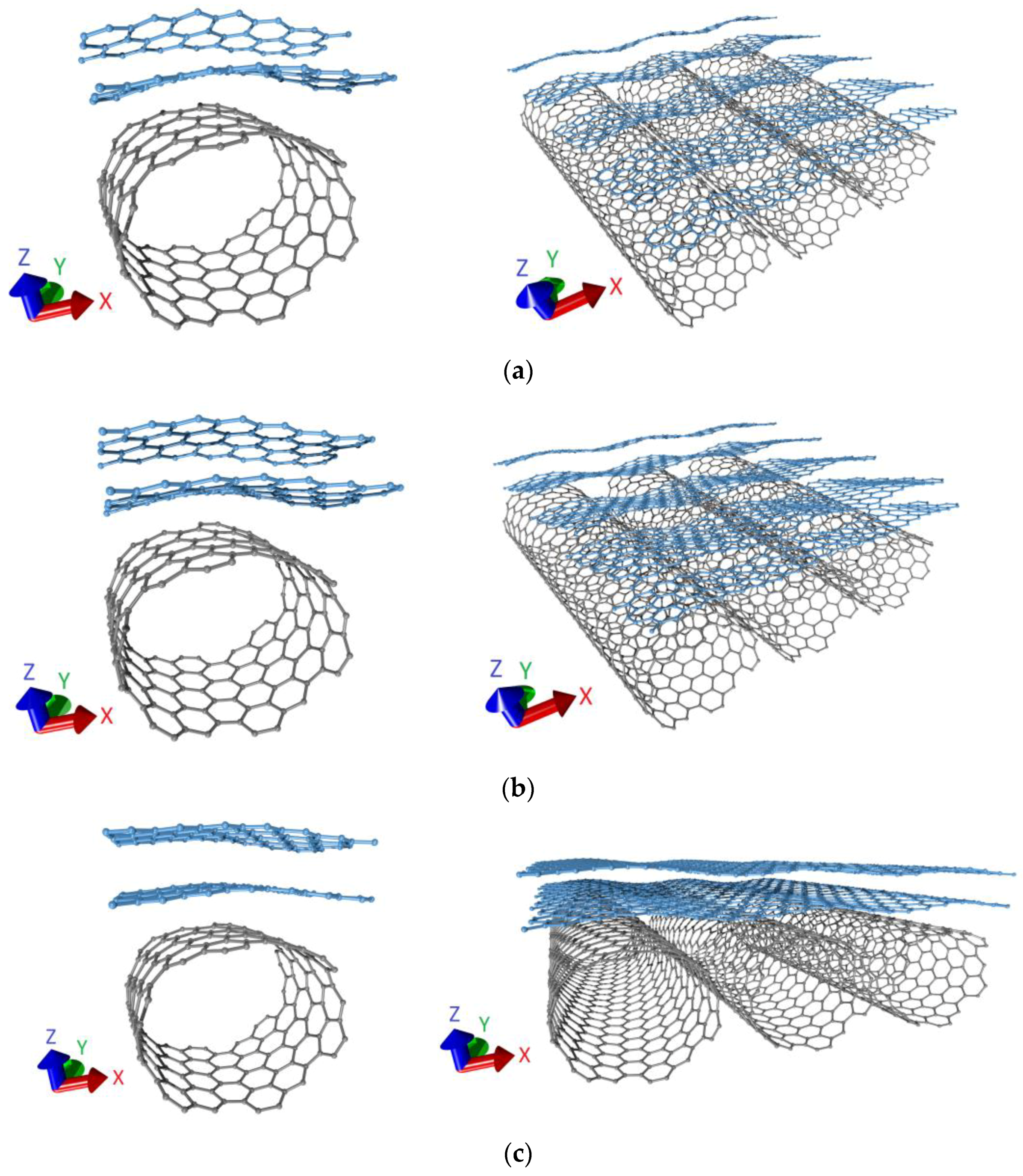
3.1. Atomic Structure of Supercells of Graphene-SWCNT (12,6) Hybrid

In this study, we considered three atomic models of hybrid 2D structures based on graphene and SWCNT. They are formed by AB-stacked bilayer graphene and (12,6) SWCNTs of ~1.2 nm in diameter. The AB-stacked graphene bilayer was located above the nanotube in a supercell, forming the so-called “islands” of increased carbon density in the hybrid structure, corresponding to the experimental data [39]. These models were selected based on the results of our previous study [40]. It was shown that the considered topological models are thermodynamically stable at room temperature [40]. The thermodynamic stability was estimated from the binding energy Eb, which was calculated as the difference between the hybrid film energy and the energies of the isolated graphene bilayer and SWCNT (12,6). The calculated values of Eb were negative for all considered atomic models, so the constructed supercells are favorable in terms of energy.
The difference between the atomic models consisted in the size of the graphene fragment along the Y axis (in the direction of the armchair of the graphene sheet) and the displacement of one graphene layer relative to the other along the Y axis. We considered atomistic models with a length of graphene fragment along the Y axis of two hexagons or 0.5 nm (model V1); three hexagons, or 0.71 nm (model V2); and four hexagons, or 0.92 nm (model V3). The displacement of one graphene layer relative to the other along the Y axis was 0.48 nm for model V1, 0.27 nm for model V2, and 0.06 nm for model V3. In all atomic models, the graphene layers were located at a distance of ~0.3 nm from each other along the Z axis (perpendicular to the nanotube axis). The distance between the bilayer graphene and the nanotube was also ~0.3 nm. Translation vectors of supercells of atomic models were the following: Lx = 1.71 nm and Ly = 1.13 nm for model V1; Lx = 1.70 nm and Ly = 1.11 nm for model V2; and Lx = 1.72 nm and Ly = 1.13 nm for model V3. Figure 1 shows the equilibrium configurations of supercells of models V1, V2, and V3. Expanded fragments of the studied atomic models obtained by multiple translations of supercells along the X and Y axes are also shown in the Figure 1.
To build atomic models of graphene-nanotube hybrid films, (12,6) SWCNTs of ~1.2 nm in diameter were chosen since they are high purity (over 90%) SWCNTs, which are often obtained in a real experiment [41]. The metallic conductivity type of (12,6) SWCNTs determines their prospects for use as electrodes in flexible electronic devices [42]. The bilayer graphene was used in atomic models of graphene-SWСNT hybrid films because multilayer graphene is more stable than monolayer graphene in real experiments.

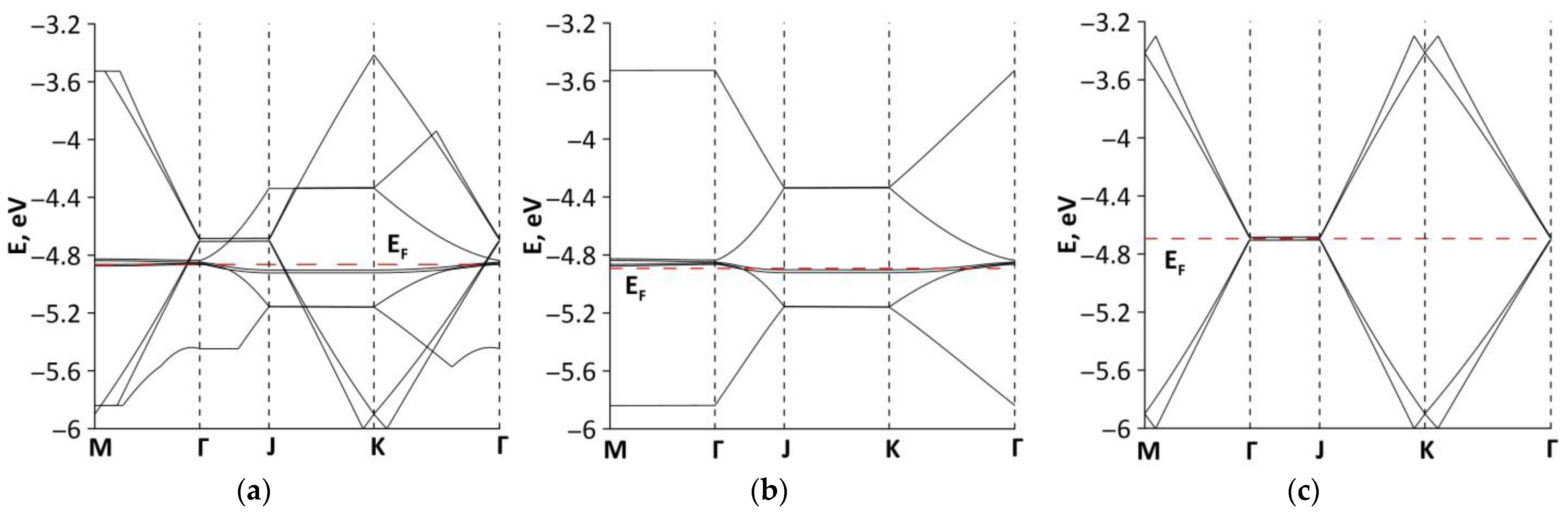
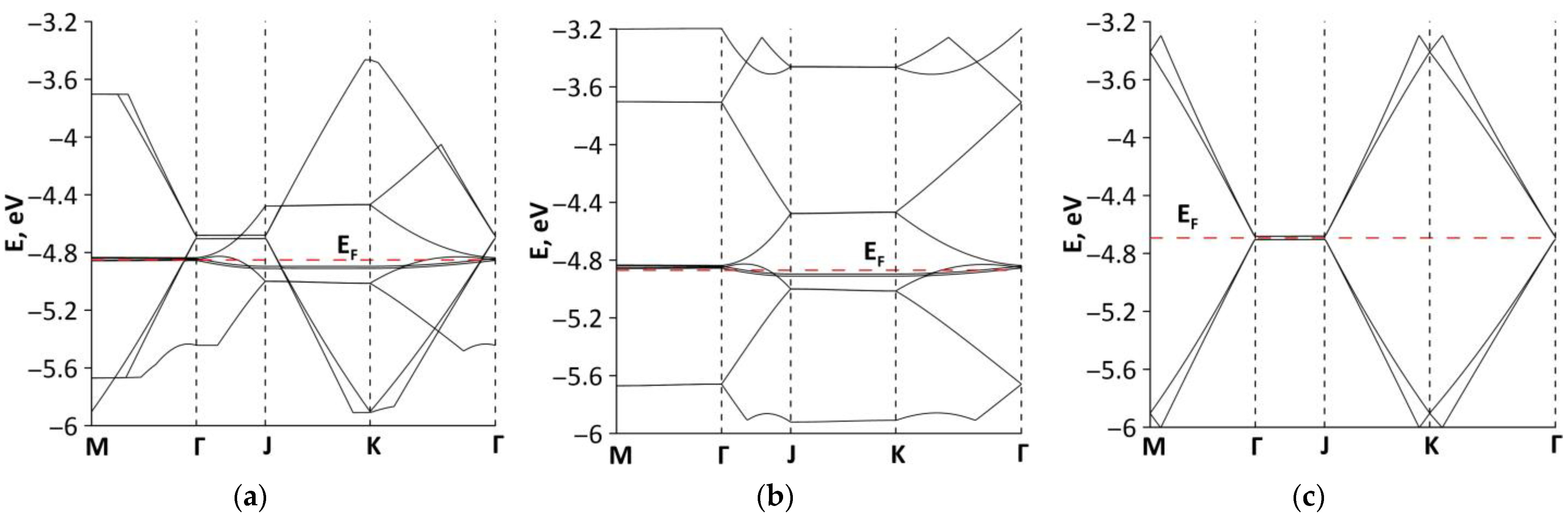
3.2. Electronic Structure of Graphene-SWCNT (12,6) Hybrid Films

To reveal the electronic structure features of graphene-SWСNT (12,6) hybrid films, we carried out calculations of the band structure in the basis of atomic p-orbitals. The first Brillouin zone was a rectangle. The band structure was sampled along a path M–Г–J–K–Г within the first Brillouin zone. Figure 2, Figure 3 and Figure 4 show band diagrams of models V1, V2, and V3 of graphene–SWCNT (12,6) hybrid films near the Fermi level EF, since it is the electronic states at the Fermi level that make the decisive contribution to the conductive properties of the material. To understand the patterns of the electronic structure formation for graphene-nanotube hybrids, these figures show fragments of the band structures of SWCNT (12,6) and AB-stacked bilayer graphene, which are part of hybrid film.
An analysis of band diagrams shows that bilayer graphene makes a decisive contribution to the formation of the energy subband profile near the valence band maximum (VBM) and the conduction band minimum (CBM) of graphene-SWCNT (12,6) hybrid. In the case of atomic models V1 and V2, the band diagrams of graphene-SWСNT (12,6) hybrid films and bilayer graphene fragments are similar. It can be noted that there is no energy gap in the band structure of models V1 and V2. The notable changes in the band diagram near the VBM and CBM are observed both for bilayer graphene and for graphene-SWСNT (12,6) hybrid film for the model V3. For a fragment of bilayer graphene, an energy gap of ~0.1 eV opens between the highly symmetrical points K and Г of the Brillouin zone. In the band structure of graphene-SWСNT (12,6) hybrid film, an energy gap of ~0.1 eV also appears between the highly symmetrical points K and Г of the Brillouin zone. The band diagrams of nanotube (12,6) in the supercell of models V1, V2, and V3 are similar, but the energy gap between the VBM and CBM of model V3 is larger than that of the V1 and V2. A possible reason for the differences in the values of the energy gap is related to the different orientation of the graphene bilayer with respect to the surface of the nanotube. In the case of models V1 and V2, a bilayer graphene fragment is oriented at an angle to the nanotube surface. In model V3, a bilayer graphene fragment is located strictly horizontally above the nanotube.

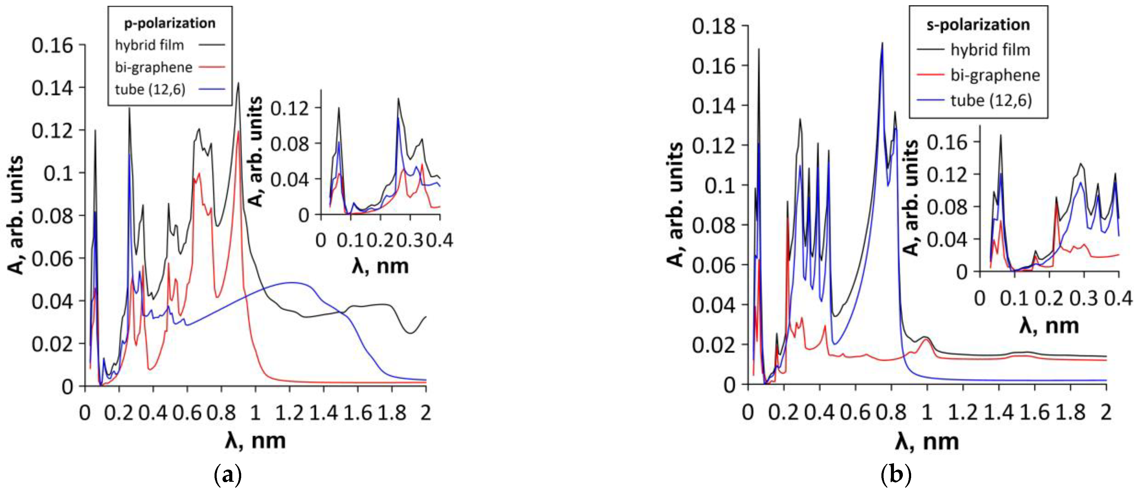
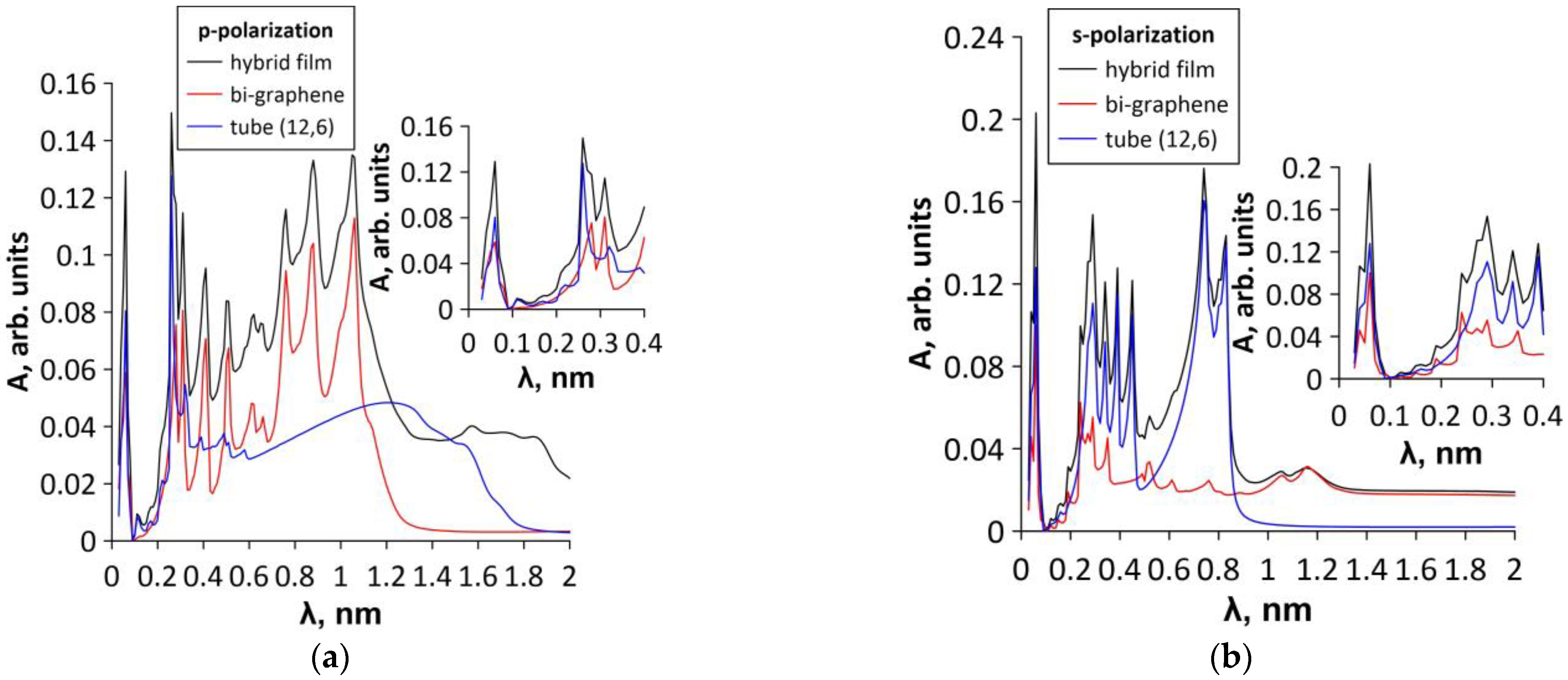
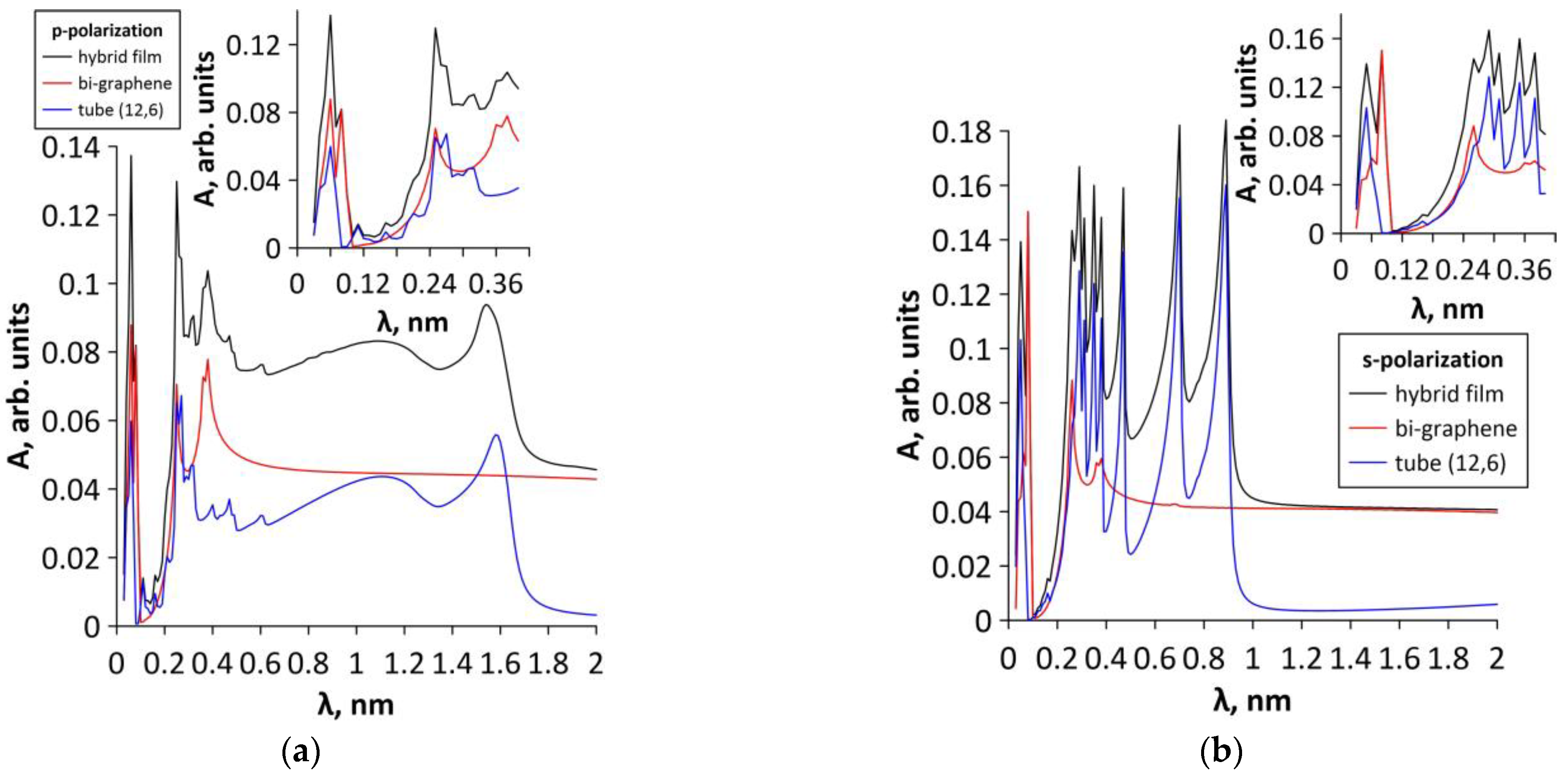
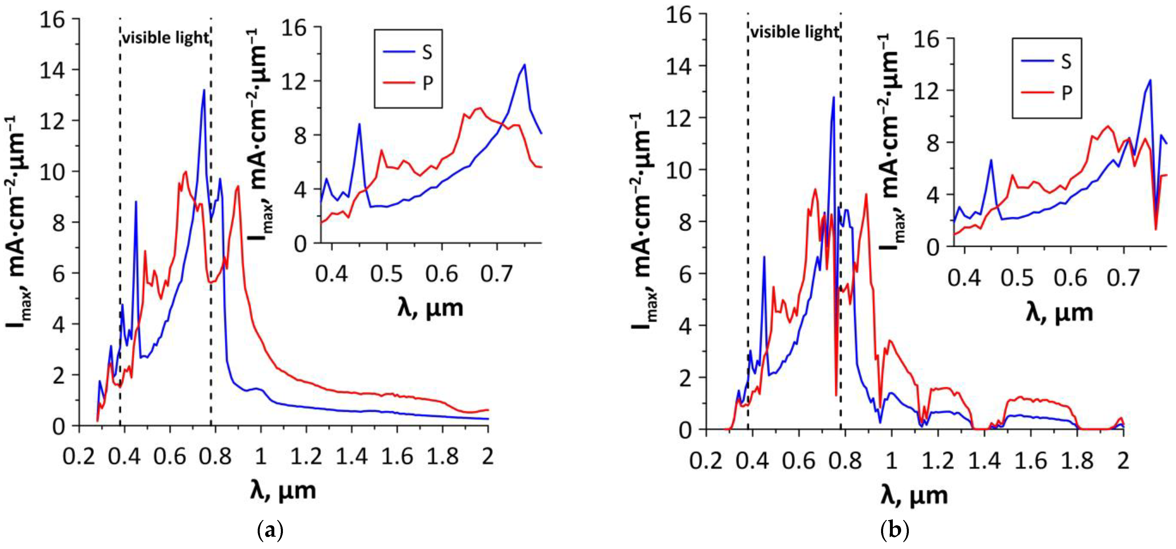
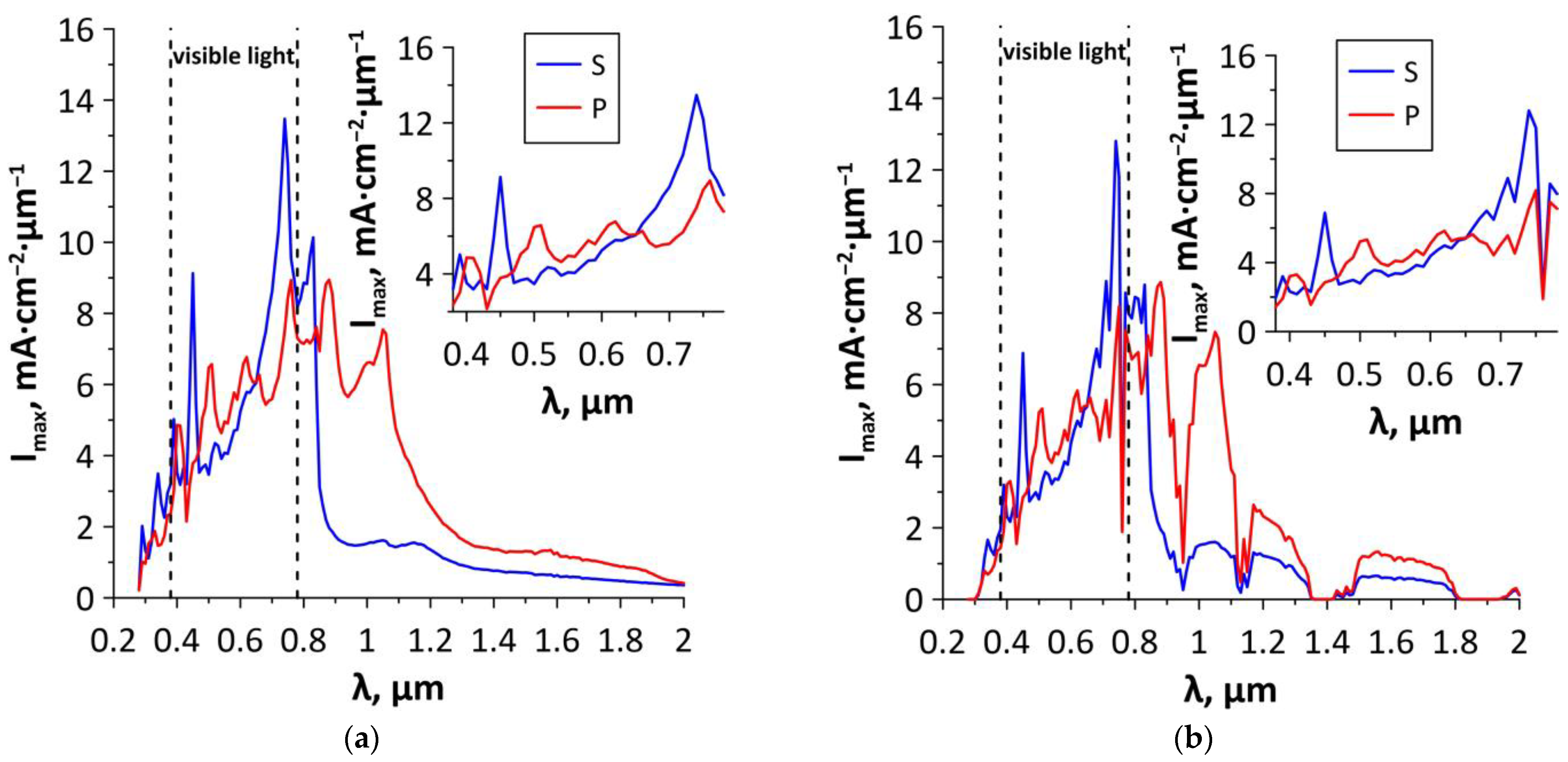
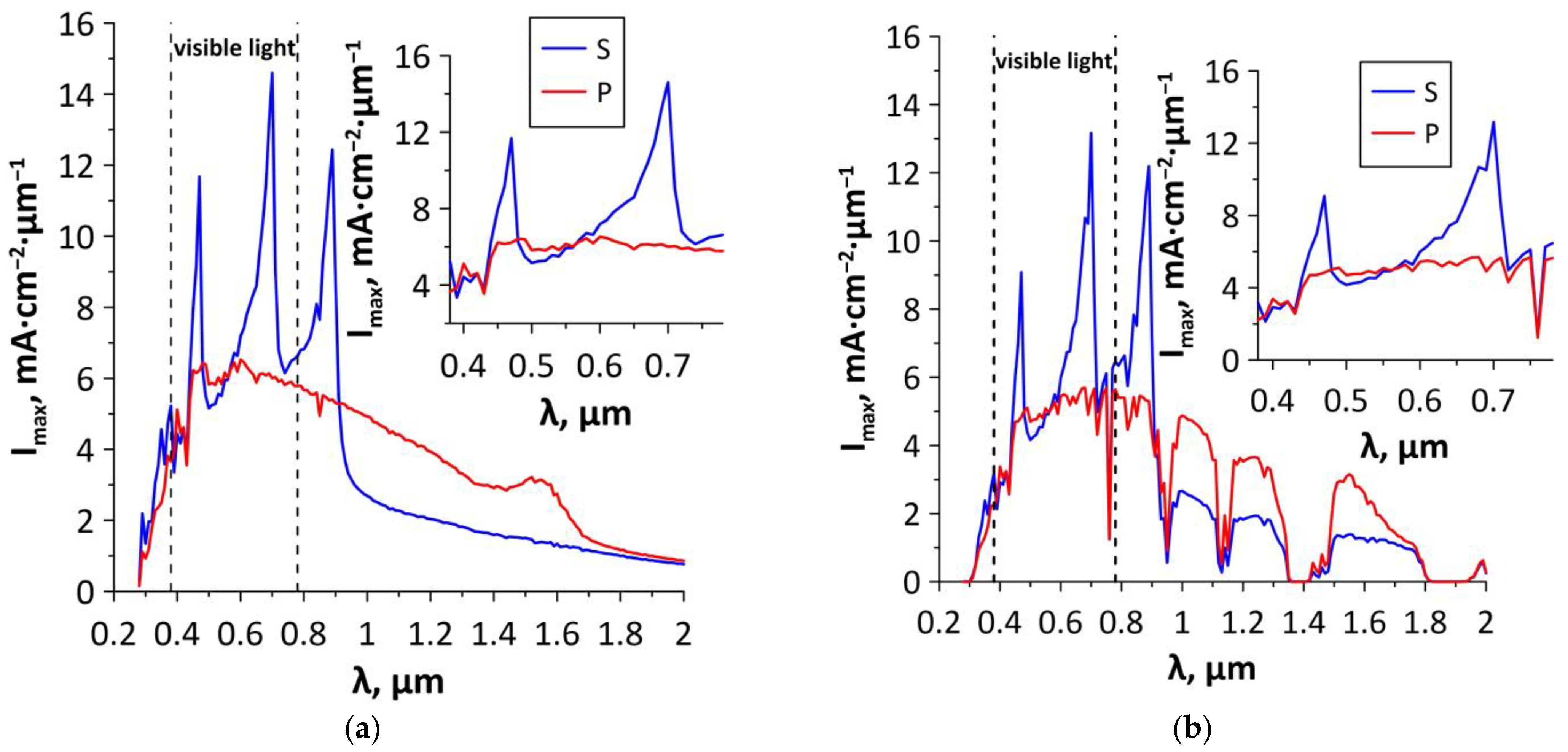
3.3. Optical and Optoelectronic Properties of Graphene-SWCNT (12,6) Hybrid Films

An analysis of optical properties was carried out on the basis of the results of calculating the absorption coefficient A in the wavelength range of the UV-, visible and near-IR radiation (0.02–2 μm). Two cases of electromagnetic radiation polarization are considered: along the X axis (p-polarization) and along the Y axis (s-polarization). Figure 5, Figure 6 and Figure 7 show the spectral profiles of the absorption coefficient A for the considered models V1, V2, and V3, respectively. For the p-polarized wave, the optical absorption profile of model V1 has two distinct peaks with a maximum absorption value of ~12% in the visible wavelength range, one maximum of ~14.3% in the near-IR range, and three maxima in the near-UV range with a maximum absorption value ~13.1%. The main contribution in the visible range is made by bilayer graphene, while in the IR range, the contribution of SWCNTs (12,6) dominates, which is especially noticeable in the range of 1–2 µm. In the UV range, the contribution of both SWCNTs (12,6) and bilayer graphene is noticeable; therefore, absorption is enhanced due to a synergistic effect. At the same time, the optical absorption profile for the V1 model with an s-polarized wave has a different form than for a p-polarized wave. The main contribution in the visible range is made by SWCNT (12,6): the optical absorption profile for graphene-SWCNT (12,6) hybrid film almost completely coincides with the absorption profile for SWCNTs (12,6). The maximum absorption value is ~17%. In the IR range, bilayer graphene makes the main contribution, since SWCNT (12,6) demonstrates almost complete transparency for this wavelength range. In the UV range, an increase in absorption is observed in comparison with individual bilayer graphene and SWCNTs (12,6), as for the p-polarized wave.
The absorption coefficient profile for model V2 in the case of a p-polarized wave is somewhat similar to the absorption coefficient profile for model V1. The IR range is rich in absorption peaks with a maximum value of about 13.8%. In the range from 1.2 μm to 2 μm, the contribution of (12,6) SWCNTs dominates, and bilayer graphene has an absorption coefficient of less than 1%. In the visible range, four absorption peaks are observed with the largest value of ~11.6%; here, bilayer graphene makes the main contribution. In the UV range, there is a peak characteristic of graphene and CNTs at a wavelength of ~0.256 μm. In the case of an s-polarized wave, the absorption coefficient profile of model V2 is similar to the absorption profile for the V1 model. Here, in the visible region, the (12,6) SWCNTs make the main contribution, and in the IR region, the bilayer graphene makes the main contribution, almost completely repeating the absorption coefficient profile of the graphene-SWCNT (12,6) hybrid film. In the UV range, there are many absorption peaks with a maximum value of about 15.7% due to the presence of (12,6) SWCNTs in the hybrid film. For the p-polarized wave, the absorption coefficient profile for model V3 differs significantly from the absorption coefficient profile of models V1 and V2. In practically all studied radiation ranges, the contribution of both bilayer graphene and (12,6) SWCNTs dominates. In the IR region, a peak with a height of ~9.5% is observed. In the UV region, as before, absorption is enhanced due to the addition of bilayer graphene and (12,6) SWCNTs peaks with a resulting absorption of ~13.9%. In the case of an s-polarized wave, model V3 shows one peak in the IR range, three peaks in the visible range, and three peaks in the UV range. The maximum absorption in this case is ~18.4%. The main contribution to the absorption in the visible range and partially in the IR range is made by (12,6) SWСNTs. The main contribution to the absorption in the IR range is made by bilayer graphene.
Let us turn to the analysis of the optoelectronic properties of the investigated graphene-SWCNT (12,6) hybrid films. The photocurrent spectra are calculated based on the obtained absorption spectra and solar radiation spectra on the earth’s surface (AM1.5) and outside the earth’s atmosphere (AM0). Solar radiation spectra AM0 and AM1.5 were taken from the website of the National Renewable Energy Laboratory [43], where the solar spectra are given in the wavelength range 280–2000 nm. The photocurrent spectra of models V1, V2, and V3 are shown in Figure 8, Figure 9 and Figure 10. The photocurrent values are shown in the figures for a surface area of 1 cm2. Table 1 shows the calculated integral values of the photocurrent for the entire solar radiation spectrum, the visible range of the solar spectrum 380–780 nm, and the maximum value of the photocurrent at a wavelength of 550 nm, which corresponds to the maximum power of solar radiation.
The photocurrent spectrum of model V1 wave without the atmosphere (AM0) has one maximum in the IR range at a wavelength of 0.9 μm for the p-polarized wave, and at a wavelength of 0.82 μm for the s-polarized wave. Starting from a wavelength of ~0.9 μm and more, sharp drop in photocurrent occurs both for the s-and p-polarized waves due to low absorption in this wavelength range. In the visible region of the spectrum in the case of a p-polarized wave, there are two photocurrent peaks at wavelengths of 0.49 μm, and 0.67 μm. The highest photocurrent value (9.9 mA∙cm−2∙μm−1) is achieved at a wavelength of 0.67 μm with a maximum integral photocurrent value of 2.47 mA/cm2. In the case of an s-polarized wave, a photocurrent minimum is observed at a wavelength of 0.47 μm and a sharp photocurrent peak of 13.2 mA∙cm−2∙μm−1 at a wavelength of 0.75 μm. Due to the peak in the visible range, the value of the maximum integrated photocurrent is 2.29 mA/cm2, which is somewhat less for the case of a p-polarized wave. In general, for the V1 model, the case of a p-polarized wave is preferable since, in the case of an s-polarized wave, the photocurrent generation is ~38% less. A similar picture is also observed when the earth’s atmosphere (AM1.5) is taken into account, where the generation of photocurrent is less intense (by ~37%) for the s-polarized wave than for the p-polarized wave.
In the IR range, the photocurrent spectrum of model V2 for solar spectrum AM0 has high peak of 10.13 mA∙cm−2∙μm−1 at 0.83 μm in the case of s-polarization, and two high peaks in the case of p-polarization (8.94 mA∙cm−2∙μm−1 at 0.88 μm and 7.54 mA∙cm−2∙μm−1 at 1.05 μm). In the presence of an atmosphere (AM1.5), solar radiation power minima do not affect this region. In the visible range, both the photocurrent spectra for AM0 and AM1.5 solar spectra have two high peaks at 0.45 μm and at 0.74 μm in the case of s-polarized wave as for model V1. In the case of s-polarized wave, there are no clear maxima of photocurrent generation, the spectral profile is quite indented. The integral value of the photocurrent for visible radiation is 2.46 mA/cm2 for the case of s-polarization versus 2.22 mA/cm2 for the case of p-polarization.
Model V3 showed the maximum efficiency of photocurrent generation in the entire considered wavelength range, both for p- and s-polarizations. The integral value of the photocurrent for the entire solar spectrum in the case of the p-polarized wave is 6.4 mA/cm2, and in the case of the s-polarized wave it is 6.07 mA/cm2. This indicator is the highest among the three considered models, both for the case of AM0 and AM1.5 solar spectra. Both for AM0 and AM1.5 solar spectra, the pronounced ability to generate the photocurrent of the model V3 is due to two peaks (11.67 mA∙cm−2∙μm−1 at 0.47 μm and 14.6 mA∙cm−2∙μm−1 at 0.7 μm) for a s-polarized wave. All of the above (for model V3) also applies to the integral value of the photocurrent for the visible radiation spectrum. Here, a p-polarized wave is capable of generating up to 2.86 mA/cm2 of photocurrent, but in the case of an s-polarized wave, the generation efficiency decreases to 2.33 mA/cm2.

4. Conclusions

A predictive study of the electronic structure, optical, and optoelectronic properties of graphene-SWСNT (12,6) hybrid films with an island-type topology was performed. The regularities of the band structure, the optical absorption coefficient spectrum, and the photocurrent spectrum in the UV, visible, and near-IR ranges were revealed for three atomic models of graphene-SWCNT films. It was found that bilayer graphene makes a decisive contribution to the energy subband profile near the VBM and CBM of a graphene-SWCNT (12,6) hybrid. The band structure of the graphene-SWСNT (12,6) hybrid for model V3 exhibits an energy gap of ~0.1 eV. The absorption coefficient profile for the V3 model in the case of a p-polarized wave differs significantly from the absorption coefficient profile for the models V1 and V2. In almost the entire studied radiation range, the contributions of both bilayer graphene and (12,6) SWCNTs dominate. Thus, when analyzing the values of the integral photocurrent both for the visible region and for the entire spectrum of solar radiation, the most effective implementation of graphene-SWCNT (12,6) hybrid film is model V3, where in the case of p-polarization the value of the integral photocurrent reaches 6.4 mA∙cm−2∙μm−1. The V1 model has the lowest efficiency in the IR region, where it demonstrated the almost complete absence of photocurrent generation. Model V2, on the contrary, is more susceptible to the IR range.

Author Contributions

Conceptualization, O.E.G. and M.M.S.; methodology, O.E.G. and M.M.S.; funding acquisition, O.E.G., M.M.S., P.V.B., and D.A.K.; investigation, O.E.G., D.A.K., P.V.B., and M.M.S.; validation, D.A.K.; visualization, P.V.B. and M.M.S.; writing—original draft preparation, D.A.K. and P.V.B.; writing—review and editing, O.E.G. and M.M.S. All authors have read and agreed to the published version of the manuscript.

Funding

The research was funded by the Council on grants of the President of the Russian Federation (project No. МК-2289.2021.1.2) and by the Ministry of Science and Higher Education of the Russian Federation (project No. FSRR-2023-0008).

Data Availability Statement

Not applicable.

Conflicts of Interest

The authors declare no conflict of interest.

References

  1. Zhang, F.; Yang, K.; Liu, G.; Chen, Y.; Wang, M.; Li, S.; Li, R. Recent advances on graphene: Synthesis, properties and applications. Compos. Part A Appl. Sci. Manuf. 2022, 160, 107051. [Google Scholar] [CrossRef]
  2. Rathinavel, S.; Priyadharshini, K.; Panda, D. A review on carbon nanotube: An overview of synthesis, properties, functionalization, characterization, and the application. Mater. Sci. Eng. B. 2021, 268, 115095. [Google Scholar] [CrossRef]
  3. Zhang, J.; Peng, H.; Zhang, H.; Maruyama, S.; Lin, L. The Roadmap of Graphene: From Fundamental Research to Broad Applications. Adv. Funct. Mater. 2022, 32, 2208378. [Google Scholar] [CrossRef]
  4. Venkataraman, A.; Amadi, E.V.; Chen, Y.; Papadopoulos, C. Carbon Nanotube Assembly and Integration for Applications. Nanoscale Res. Lett. 2019, 14, 220. [Google Scholar] [CrossRef]
  5. Lee, C.; Wei, X.D.; Kysar, J.W.; Hone, J. Measurement of the Elastic Properties and Intrinsic Strength of Monolayer Graphene. Science 2008, 321, 385–388. [Google Scholar] [CrossRef] [PubMed]
  6. Stankovich, S.; Dikin, D.A.; Piner, R.D.; Kohlhaas, K.A.; Kleinhammes, A.; Jia, Y.; Wu, Y.; Nguyen, S.T.; Ruoff, R.S. Synthesis of Graphene-Based Nanosheets via Chemical Reduction of Exfoliated Graphite Oxide. Carbon 2007, 45, 1558–1565. [Google Scholar] [CrossRef]
  7. Wilhite, P.; Vyas, A.A.; Tan, J.; Tan, J.; Yamada, T.; Wang, P.; Park, J.; Yang, C.Y. Metal–nanocarbon contacts. Semicond. Sci. Technol. 2014, 29, 054006. [Google Scholar] [CrossRef]
  8. Du, W.; Ahmed, Z.; Wang, Q.; Yu, C.; Feng, Z.; Li, G.; Zhang, M.; Zhou, C.; Senegor, R.; Yang, C.Y. Structures, properties, and applications of CNT-graphene heterostructures. 2D Mater. 2019, 6, 042005. [Google Scholar] [CrossRef]
  9. Fan, W.; Longsheng, Z.; Tianxi, L. Graphene-Carbon Nanotube Hybrids for Energy and Environmental Applications, 1st ed.; Springer: Singapore, 2017; pp. 21–51. [Google Scholar]
  10. Lv, R.; Cruz-Silva, E.; Terrones, M. Building Complex Hybrid Carbon Architectures by Covalent Interconnections: Graphene-Nanotube Hybrids and More. ACS Nano 2014, 8, 4061–4069. [Google Scholar] [CrossRef]
  11. Li, Y.G.; Zhou, W.; Wang, H.L.; Xie, L.M.; Liang, Y.Y.; Wei, F.; Idrobo, J.C.; Pennycook, S.J.; Dai, H.J. An Oxygen Reduction Electrocatalyst Based on Carbon Nanotube-Graphene Complexes. Nat. Nanotechnol. 2012, 7, 394–400. [Google Scholar] [CrossRef]
  12. Kim, S.H.; Song, W.; Jung, M.W.; Kang, M.A.; Kim, K.; Chang, S.J.; Lee, S.S.; Lim, J.; Hwang, J.; Myung, S.; et al. Carbon nanotube and graphene hybrid thin film for transparent electrodes and field effect transistors. Adv. Mater. 2014, 26, 4247–4252. [Google Scholar] [CrossRef]
  13. Shi, E.; Li, H.; Yang, L.; Hou, J.; Li, Y.; Li, L.; Cao, A.; Fang, Y. Carbon nanotube network embroidered graphene films for monolithic all-carbon electronics. Adv. Mater. 2015, 27, 682–688. [Google Scholar] [CrossRef] [PubMed]
  14. Kholmanov, I.N.; Magnuson, C.W.; Piner, R.; Kim, J.Y.; Aliev, A.E.; Tan, C.; Kim, T.Y.; Zakhidov, A.A.; Sberveglieri, G.; Baughman, R.H.; et al. Optical, electrical, and electromechanical properties of hybrid graphene/carbon nanotube films. Adv. Mater. 2015, 27, 3053–3059. [Google Scholar] [CrossRef]
  15. Etesami, M.; Nguyen, M.T.; Yonezawa, T.; Tuantranont, A.; Somwangthanaroj, A.; Kheawhom, S. 3D carbon nanotubes-graphene hybrids for energy conversion and storage applications. Chem. Eng. J. 2022, 446, 137190. [Google Scholar] [CrossRef]
  16. Zang, X.; Jiang, Y.; Sanghadasa, M.; Lin, L. Chemical vapor deposition of 3D graphene/carbon nanotubes networks for hybrid supercapacitors. Sens. Actuator A Phys. 2020, 304, 111886. [Google Scholar] [CrossRef]
  17. Yuan, G.-J.; Xie, J.-F.; Li, H.-H.; Shan, B.; Zhang, X.-X.; Liu, J.; Li, L.; Tian, Y.-Z. Thermally Reduced Graphene Oxide/Carbon Nanotube Composite Films for Thermal Packaging Applications. Materials 2020, 13, 317. [Google Scholar] [CrossRef] [PubMed]
  18. Advincula, P.A.; Beckham, J.L.; Choi, C.H.; Chen, W.; Han, Y.; Kosynkin, D.V.; Lathem, A.; Mayoral, A.; Yacaman, M.J.; Tour, J.M. Tunable Hybridized Morphologies Obtained through Flash Joule Heating of Carbon Nanotubes. ACS Nano 2023, 17, 2506–2516. [Google Scholar] [CrossRef] [PubMed]
  19. Li, Y.Y.; Ai, Q.Q.; Mao, L.N.; Guo, J.X.; Gong, T.X.; Lin, Y.; Wu, G.T.; Huang, W.; Zhang, X.S. Hybrid strategy of graphene/carbon nanotube hierarchical networks for highly sensitive, flexible wearable strain sensors. Sci. Rep. 2021, 11, 21006. [Google Scholar] [CrossRef]
  20. Zhang, Y.; Li, Y.; Sun, J.; You, Q.; Li, K.; Zhu, M.; Deng, T. A Micro Broadband Photodetector Based on Single Wall Carbon Nanotubes-Graphene Heterojunction. J. Light. Technol. 2022, 40, 149–155. [Google Scholar] [CrossRef]
  21. Zhang, Y.; Li, Y.; You, Q.; Sun, J.; Li, K.; Hong, H.; Kong, L.; Zhu, M.; Deng, T.; Liu, Z. A broadband 3D microtubular photodetector based on a single wall carbon nanotube–graphene heterojunction. Nanoscale 2023, 15, 1402–1411. [Google Scholar] [CrossRef]
  22. Alamri, M.; Liu, B.; Berrie, C.L.; Walsh, M.; Wu, J.Z. Probing the role of CNTs in Pt nanoparticle/CNT/graphene nanohybrids H2 sensors. Nano Express 2022, 3, 035004. [Google Scholar] [CrossRef]
  23. Zhao, W.; Ghaznavi, A.; Gao, Y.; Wu, M.; Xu, J. Synthesis of a Functionalized Carbon Nanotube Graphene Composite Enabling pH-Responsive Electrochemical Sensing for Biomedical Applications. ACS Appl. Electron. Mater. 2023, 5, 1224–1233. [Google Scholar] [CrossRef]
  24. Ho, Y.H.; Chiu, Y.H.; Lu, J.M.; Lin, M.F. Low-energy electronic structures of nanotube–Graphene hybrid carbon systems. Phys. E 2010, 42, 744–747. [Google Scholar] [CrossRef]
  25. Cook, B.G.; French, W.R.; Varga, K. Electron transport properties of CNT–graphene contacts. Appl. Phys. Lett. 2012, 101, 153501. [Google Scholar] [CrossRef]
  26. Akhukov, M.A.; Yuan, S.; Fasolino, A.; Katsnelson, M.I. Electronic, magnetic and transport properties of graphene ribbons terminated by nanotubes. New J. Phys. 2012, 14, 123012. [Google Scholar] [CrossRef]
  27. Ivanovskaya, V.V.; Zobelli, A.; Wagner, P.; Heggie, M.I.; Briddon, P.R.; Rayson, M.J.; Ewels, C.P. Low-Energy Termination of Graphene Edges via the Formation of Narrow Nanotube. Phys. Rev. Lett. 2011, 107, 065502. [Google Scholar] [CrossRef]
  28. Artyukh, A.A.; Chernozatonskii, L.A.; Sorokin, P.B. Mechanical and electronic properties of carbon nanotube–graphene compounds. Phys. Status Solidi B 2010, 247, 2927. [Google Scholar] [CrossRef]
  29. Slepchenkov, M.M.; Glukhova, O.E. Mechanical and Electroconductive Properties of Mono- and Bilayer Graphene–Carbon Nanotube Films. Coatings 2019, 9, 74. [Google Scholar] [CrossRef]
  30. Slepchenkov, M.M.; Mitrofanov, V.V.; Nefedov, I.S.; Glukhova, O.E. Electrical and Photovoltaic Properties of Layered Composite Films of Covalently Bonded Graphene and Single-Walled Carbon Nanotubes. Coatings 2020, 10, 324. [Google Scholar] [CrossRef]
  31. Elstner, M.; Seifert, G. Density functional tight binding. Phil. Trans. R. Soc. A 2014, 372, 20120483. [Google Scholar] [CrossRef]
  32. DFTB+ Density Functional based Tight Binding (and More). Available online: https://dftbplus.org/ (accessed on 12 May 2022).
  33. Mulliken, R.S. Electronic Population Analysis on LCAO–MO Molecular Wave Functions I. J. Chem. Phys. 1955, 23, 1833. [Google Scholar] [CrossRef]
  34. Marder, M. Condensed Matter Physics, 2nd ed.; John Wiley & Sons: Hoboken, NJ, USA, 2010; pp. 623–631. [Google Scholar]
  35. Calderín, L.; Karasiev, V.V.; Trickey, S.B. Kubo-Greenwood electrical conductivity formulation and implementation for projector augmented wave datasets. Comput. Phys. Commun. 2017, 221, 118–142. [Google Scholar] [CrossRef]
  36. Pedersen, T.G.; Pedersen, K.; Kriestensen, T.B. Optical matrix elements in tight-binding calculations. Phys. Rev. B 2001, 63, 201101(R). [Google Scholar] [CrossRef]
  37. Allen, P.B. Electron transport. In Conceptual Foundations of Materials, 2nd ed.; Louie, S.G., Cohen, M.L., Eds.; Elsevier Science: Amsterdam, The Netherlands, 2006; Volume 2, pp. 172–175. [Google Scholar]
  38. Glukhova, O.E.; Nefedov, I.S.; Shalin, A.S.; Slepchenkov, M.M. New 2D graphene hybrid composites as an effective base element of optical nanodevices. Beilstein J. Nanotechnol. 2018, 9, 1321–1327. [Google Scholar] [CrossRef] [PubMed]
  39. Kuang, J.; Dai, Z.; Liu, L.; Yang, Z.; Jinc, M.; Zhang, Z. Synergistic effects from graphene and carbon nanotubes endow ordered hierarchical structure foams with a combination of compressibility, super-elasticity and stability and potential application as pressure sensors. Nanoscale 2015, 7, 9252–9260. [Google Scholar] [CrossRef]
  40. Slepchenkov, M.M.; Barkov, P.V.; Glukhova, O.E. Hybrid Films Based on Bilayer Graphene and Single-Walled Carbon Nanotubes: Simulation of Atomic Structure and Study of Electrically Conductive Properties. Nanomaterials 2021, 11, 1934. [Google Scholar] [CrossRef]
  41. Zhang, S.; Kang, L.; Wang, X.; Tong, L.; Yang, L.; Wang, Z.; Qi, K.; Deng, S.; Li, Q.; Bai, X.; et al. Arrays of horizontal carbon nanotubes of controlled chirality grown using designed catalysts. Nature 2017, 543, 234–238. [Google Scholar] [CrossRef]
  42. Liu, B.; Wu, F.; Gui, H.; Zheng, M.; Zhou, C. Chirality-Controlled Synthesis and Applications of Single-Wall Carbon Nanotubes. ACS Nano 2017, 11, 31–53. [Google Scholar] [CrossRef]
  43. National Renewable Energy Laboratory (NREL). Available online: https://www.nrel.gov/ (accessed on 15 September 2022).
Figure 1. Supercells (left) and extended fragments (right) of AB-staked bilayer graphene-SWCNT (12,6) hybrid films: (a) model V1; (b) model V2; (с) model V3.
Carbon 09 00051 g001
Figure 2. Band diagrams near the Fermi level of the model V1 of graphene-SWCNT (12,6) hybrid films: (a) hybrid structure; (b) bilayer graphene; (c) SWCNT (12,6). The red dotted line shows the Fermi level.
Carbon 09 00051 g002
Figure 3. Band diagrams near the Fermi level of the model V2 of graphene-SWCNT (12,6) hybrid films: (a) hybrid structure; (b) bilayer graphene; (c) SWCNT (12,6). The red dotted line shows the Fermi level.
Carbon 09 00051 g003
Figure 4. Band diagrams near the Fermi level of the model V3 of graphene-SWCNT (12,6) hybrid films: (a) hybrid structure; (b) bilayer graphene; (c) SWCNT (12,6). The red dotted line shows the Fermi level.
Carbon 09 00051 g004
Figure 5. Profiles of the absorption coefficient A for model V1 of graphene-SWCNT (12,6) hybrid: (a) p-polarization (along the X axis) of electromagnetic wave; (b) s-polarization (along the Y axis) of electromagnetic wave. The insets to the figures show an enlarged fragment of the absorption spectrum for the UV range.
Carbon 09 00051 g005
Figure 6. Profiles of the absorption coefficient A for model V2 of graphene-SWCNT (12,6) hybrid: (a) p-polarization (along the X axis) of electromagnetic wave; (b) s-polarization (along the Y axis) of electromagnetic wave. The insets to the figures show an enlarged fragment of the absorption spectrum for the UV range.
Carbon 09 00051 g006
Figure 7. Profiles of the absorption coefficient A for model V3 of graphene-SWCNT (12,6) hybrid: (a) p-polarization (along the X axis) of electromagnetic wave; (b) s-polarization (along the Y axis) of electromagnetic wave. The insets to the figures show an enlarged fragment of the absorption spectrum for the UV range.
Carbon 09 00051 g007
Figure 8. The photocurrent spectra for model V1 of graphene-SWCNT (12,6) hybrid: (a) outside the earth’s atmosphere (AM0); (b) on the earth’s surface (AM1.5).
Carbon 09 00051 g008
Figure 9. The photocurrent spectra for model V2 of graphene-SWCNT (12,6) hybrid: (a) outside the earth’s atmosphere (AM0); (b) on the earth’s surface (AM1.5).
Carbon 09 00051 g009
Figure 10. The photocurrent spectra for topological model V3 of graphene-SWCNT (12,6) hybrid film: (a) outside the earth’s atmosphere (AM0); (b) on the earth’s surface (AM1.5).
Carbon 09 00051 g010
Table 1. Some optoelectronic characteristics of graphene-SWCNT (12,6) hybrid film at p-polarization (along the X axis) and s-polarization (along the Y axis) of electromagnetic wave.
Solar Spectrum AM0
The Integral Value of the Photocurrent for the Entire Solar Radiation Spectrum, mA/cm2Maximum Photocurrent at a Wavelength of 550 nm, mA cm−2 μm−1Integral Value of the
Photocurrent for the Visible Spectrum 380–780 nm, mA/cm2
12_6_ver_1_s 3.803.422.29
12_6_ver_1_p5.245.232.47
12_6_ver_2_s4.344.082.46
12_6_ver_2_p5.864.962.22
12_6_ver_3_s6.075.952.33
12_6_ver_3_p6.406.162.86
Solar Spectrum AM1.5
12_6_ver_1_s 2.982.831.84
12_6_ver_1_p4.094.332.02
12_6_ver_2_s3.383.372.00
12_6_ver_2_p4.564.101.80
12_6_ver_3_s4.674.912.34
12_6_ver_3_p4.755.091.89
Disclaimer/Publisher’s Note: The statements, opinions and data contained in all publications are solely those of the individual author(s) and contributor(s) and not of MDPI and/or the editor(s). MDPI and/or the editor(s) disclaim responsibility for any injury to people or property resulting from any ideas, methods, instructions or products referred to in the content.

