Article

Adsorption of Metal Atoms on SiC Monolayer

School of Automation and Information Engineering, Xi’an University of Technology, Xi’an 710048, China
*
Authors to whom correspondence should be addressed.
Inorganics 2023, 11(6), 240; https://doi.org/10.3390/inorganics11060240
Submission received: 15 May 2023 / Revised: 27 May 2023 / Accepted: 29 May 2023 / Published: 30 May 2023
(This article belongs to the Special Issue Advanced Inorganic Semiconductor Materials)

Abstract

:
The electronic, magnetic, and optical behaviors of metals (M = Ag, Al, Au, Bi, Ca, Co, Cr, Cu, Fe, Ga, K, Li, Mn, Na, Ni) adsorbed on the SiC monolayer have been calculated based on density functional theory (DFT). The binding energy results show that all the M-adsorbed SiC systems are stable. All the M-adsorbed SiC systems are magnetic with magnetic moments of 1.00 μB (Ag), 1.00 μB (Al), 1.00 μB (Au), 1.01 μB (Bi), 1.95 μB (Ca), 1.00 μB (Co), 4.26 μB (Cr), 1.00 μB (Cu), 2.00 μB (Fe), 1.00 μB (Ga), 0.99 μB (K), 1.00 μB (Li), 3.00 μB (Mn), and 1.00 μB (Na), respectively, except for the Ni-adsorbed SiC system. The Ag, Al, Au, Cr, Cu, Fe, Ga, Mn, and Na-adsorbed SiC systems become magnetic semiconductors, while Bi, Ca, Co, K, and Li-adsorbed SiC systems become semimetals. The Bader charge results show that there is a charge transfer between the metal atom and the SiC monolayer. The work function of the K-adsorbed SiC system is 2.43 eV, which is 47.9% lower than that of pristine SiC and can be used in electron-emitter devices. The Bi, Ca, Ga, and Mn-adsorbed SiC systems show new absorption peaks in the visible light range. These results indicate that M-adsorbed SiC systems have potential applications in the field of spintronic devices and solar energy conversion photovoltaic devices.

1. Introduction

Since the successful preparation of graphene [1], there has been a surge in research into two-dimensional (2D) materials, including 2D WS2 [2,3], GaN [4,5,6], BN [7,8], black phosphorus [9,10], ZnO [11,12], SiC [13,14], etc. SiC is a third-generation semiconductor material with a wide band gap, high electron saturation drift rate, high breakdown field strength, high thermal conductivity, high radiation resistance, etc. It has a wide range of applications in solar cells, high-frequency high-power devices, and high-temperature electronic devices. Two-dimensional SiC has the advantages of high electron mobility, chemical stability, and high catalytic activity and is often used to make photocatalysts [15]. Based on the first-principles approach, 2D SiC has been predicted to have a graphene-like honeycomb structure and can exist stably as a semiconductor material with a direct band gap of 2.52–2.87 eV [16,17]. Chabi et al. have successfully prepared SiC nanosheets with an average thickness of 2–3 nm through a catalytic carbon thermal reduction method and ultrasonic pretreatment process [18]. Two-dimensional SiC has great potential in the field of nanoelectronic devices, but there are some problems in photocatalysis. Two-dimensional SiC is only responsive to partially visible light [19], so it is necessary to reduce the band gap and improve the absorption efficiency of visible light. Current methods to effectively modulate the band structure include doping [20,21], stacking [22,23], adsorption [24,25], heterojunctions [26,27,28], etc.
The adsorption of metal atoms is one of the most important means to modulate the properties of 2D materials. The adsorption of different atoms on the surface of 2D materials can modulate the optical, electrical, and magnetic properties of 2D materials. Nie et al. have studied the adsorption of 3D transition metals on the SnO monolayer [29]. They found that 3D transition metal adsorption induced magnetism and achieved n-type and p-type doping. Guo et al. have modulated the electronic properties of the WSSe monolayer by adsorbing Fe, Co, and Ni atoms and developed its applications in gas sensors and single-atom catalysts [30]. Cui et al. have studied the adsorption of transition metals on the Pd2Se3 monolayer [31]. They found that the adsorption of transition metals improved light absorption in the ultraviolet, visible, and infrared regions. Xu et al. have predicted the magnetism of the SnSe2 monolayer after the adsorption of transition metals and found that the adsorption of Ti atoms can endow the SnSe2 monolayer with perpendicular magnetic anisotropy [32]. In this paper, the electronic structure, magnetic, and optical properties of 15 metal atoms adsorbed on SiC monolayer have been calculated using the first-principles approach. The influence of the M atoms on the properties of the SiC monolayer is analyzed according to the band structure, work function, and light absorption spectra, and the application prospects of M-adsorbed SiC systems in the field of spin devices and photovoltaic devices are explored.

2. Computational Details

The electronic, magnetic, and optical behaviors of M-adsorbed SiC systems have been investigated in the Vienna ab initio calculation simulation package (VASP) [33,34] using density functional theory (DFT) [35,36]. The electron-ion interactions are performed using the Perdew-Burke-Ernzerhof (PBE) form of the generalized gradient approximation (GGA) approach [37]. The exchange-correlation interactions are performed using the projector-enhanced wave (PAW) approach [38]. Dispersion corrections are considered by Grimme’s DFT-D3 method [39]. The plane wave cutoff energy is 400 eV, the Monkhorst-Pack scheme [40] grid in the Brillouin zone is 4 × 4 × 1, and the vacuum space is 20 Å. During structural relaxation, the convergences of the force and self-consistent energy are 1 × 10⁻² eV Å−1 and 1 × 10⁻⁵ eV, respectively. The optical properties are considered according to the frequency-dependent dielectric response theory, including the local field effects in the random-phase-approximation (RPA) method [41].

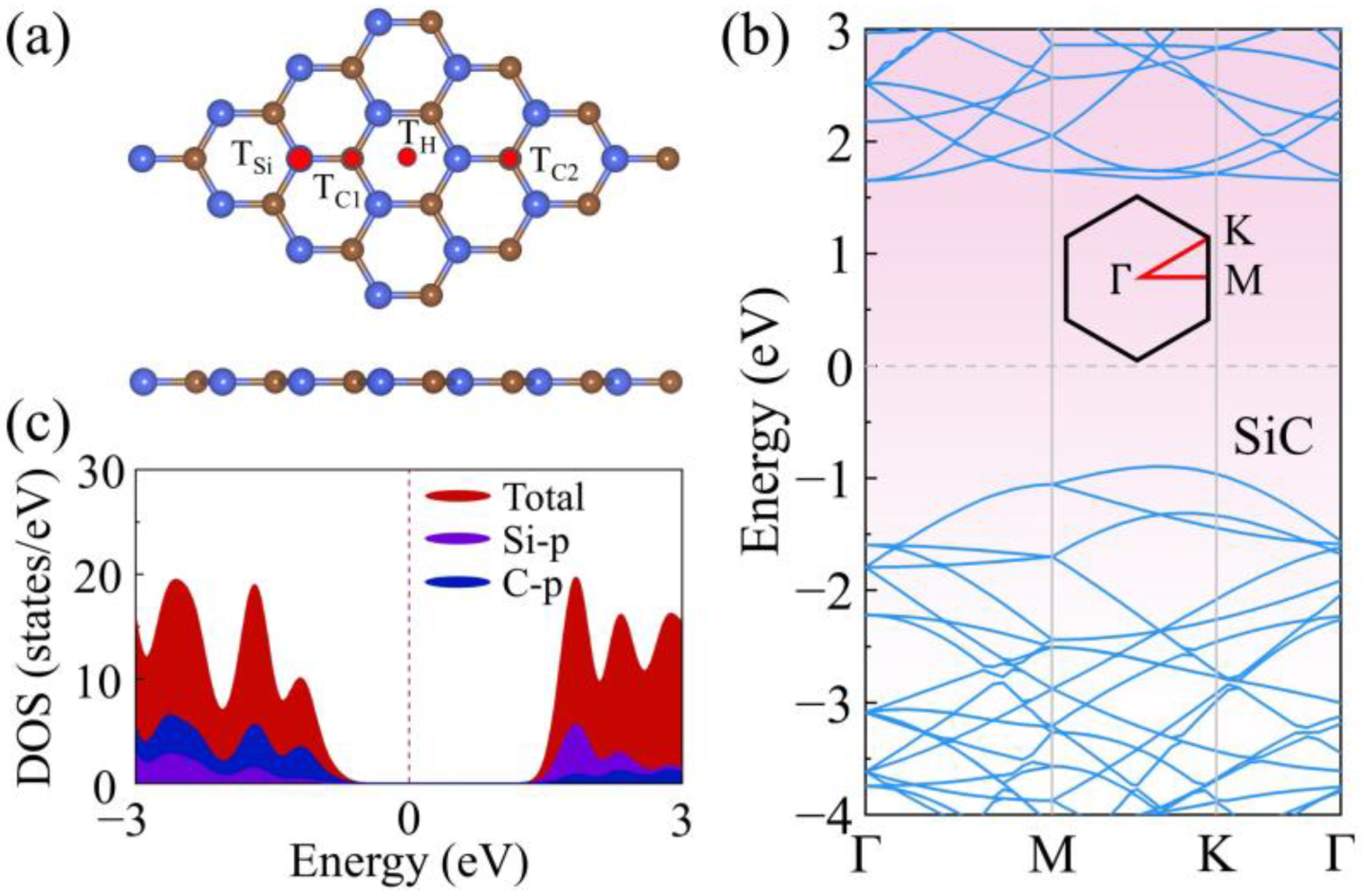
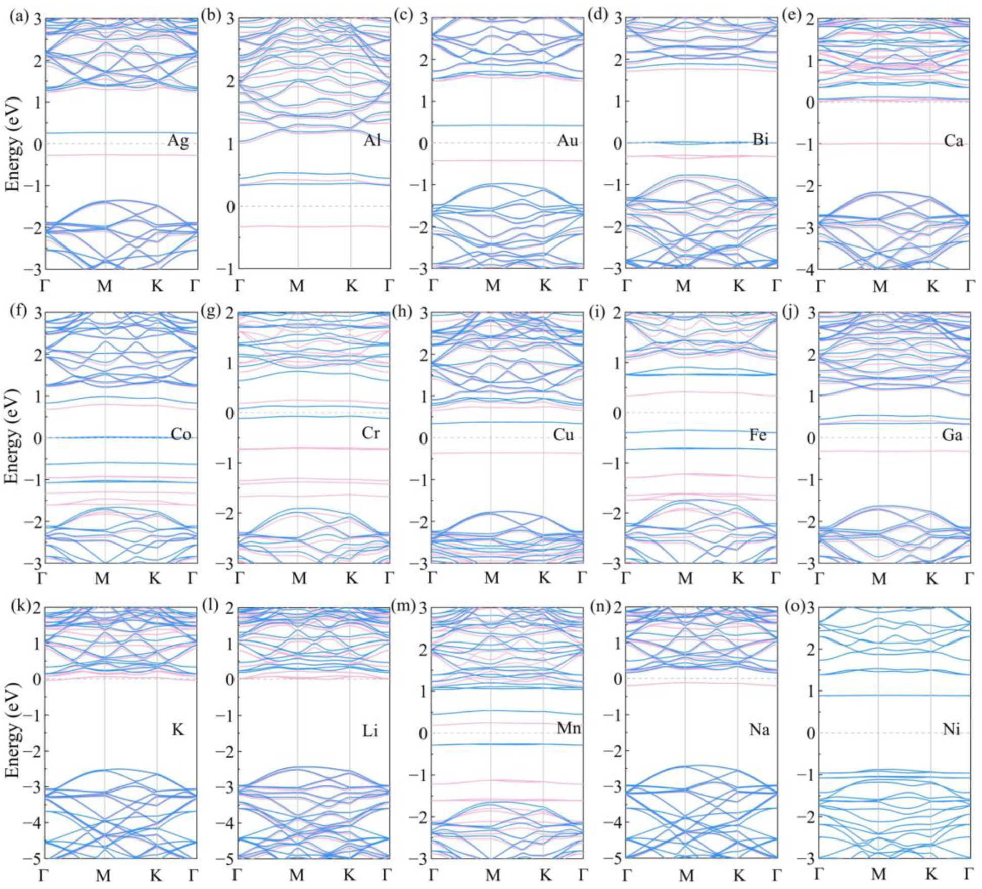
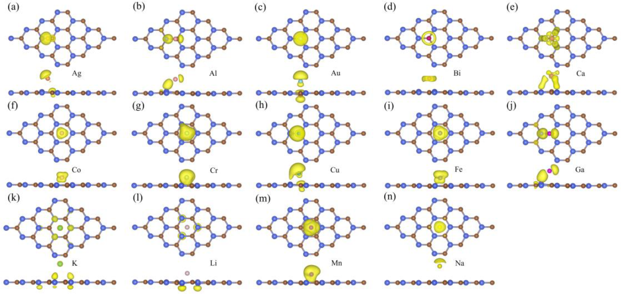
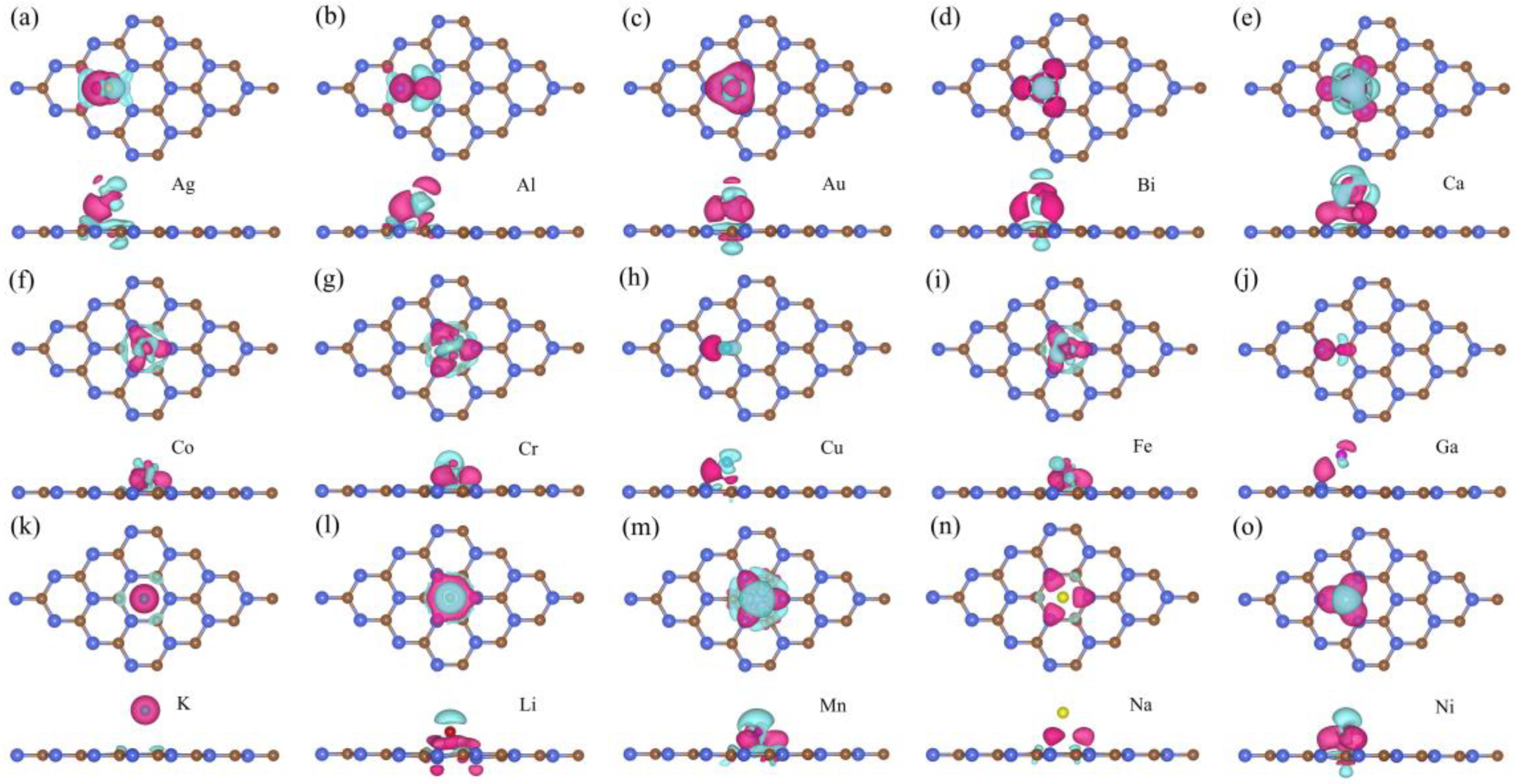
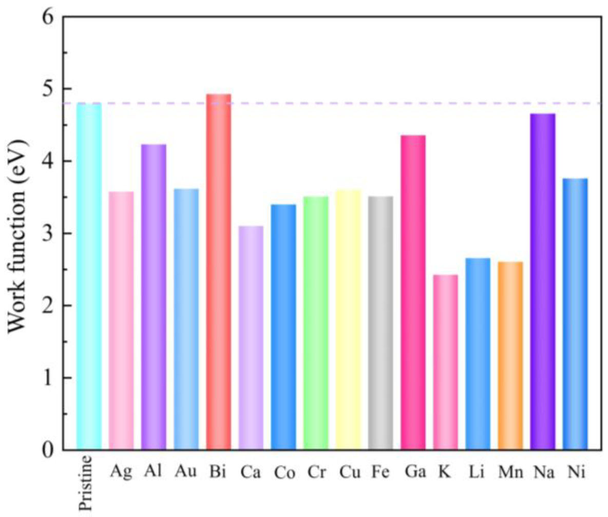
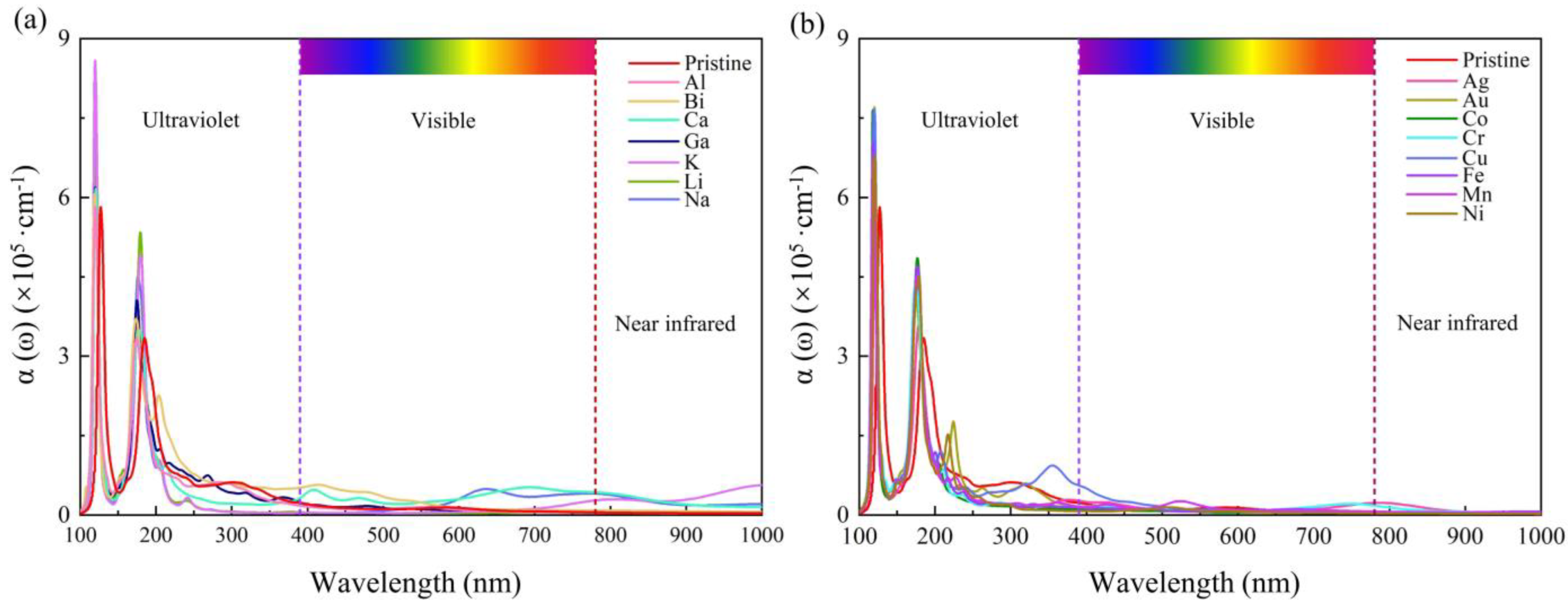
3. Results and Discussion

The pristine SiC has a graphene-like structure with an alternating arrangement of C and Si atoms, and its lattice parameter is 3.1 Å with a bond length of 1.78 Å. From the band structure and density of state (DOS) of Figure 1b,c, it can be seen that pristine SiC is a nonmagnet semiconductor with a direct bandgap of 2.5 eV, and the conduction band minimum (CBM) is mainly contributed by the hybridization of the p-state of Si and C, while the valence band maximum (VBM) is mainly contributed by the 2p-state of C. The VBM and CBM are not at the same high symmetry point, indicating that the pristine SiC is an indirect bandgap semiconductor. These results are consistent with previous reports [42], indicating that our computational method is reliable.
In order to study the stability of metal adsorption on the SiC system, we constructed four adsorption models for each type of metal, as shown in Figure 1a. The adsorption sites were located above a Si atom, above a C1 atom, above a C2 atom, and above the Si-C bond. Adsorption energy (Eads) was used to characterize the stability of the adsorption system, which can be calculated using the following formula:
Eads = EM-SiCESiCμM
where EM-SiC is the total energy of the M-adsorbed SiC systems, including the interaction energy between the metal atom and the SiC monolayer; ESiC is the energy of the pristine SiC monolayer; μM is the chemical potential of an isolated metal atom.
As listed in Table 1, the Eads of the M-adsorbed SiC systems are −0.193 eV (Ag), −1.683 eV (Al), −1.706 eV (Au), −1.135 eV (Bi), −0.111 eV (Ca), −2.785 eV (Co), −2.545 eV (Cr), −1.388 eV (Cu), −2.104 eV (Fe), −1.493 eV (Ga), −5.357 eV (K), −1.026 eV (Li), −0.956 eV (Mg), −0.301 eV (Na), and −3.845 eV (Ni), respectively. It can be seen that the Eads of all systems are negative, indicating that the systems are stable. Different metal adsorption has different adsorption sites that are the most stable. The most stable adsorption site for Ag is located at SC2, while for Co, Cr, K, Li, Mn, Na, and Ni, it is at SH. The most stable adsorption site for Al, Au, Bi, Ca, Cu, Fe, and Ga is at SC1. The interactions between different metals and the SiC monolayer are also different. The adsorption distances of the M-adsorbed SiC systems are 2.36 Å (Ag), 2.44 Å (Al), 2.04 Å (Au), 2.45 Å (Bi), 2.87 Å (Ca), 1.30 Å (Co), 1.42 Å (Cr), 2.06 Å (Cu), 1.36 Å (Fe), 2.54 Å (Ga), 3.07 Å (K), 1.61 Å (Li), 1.46 Å eV (Mg), 2.84 Å (Na), and 1.61 Å eV (Ni), respectively. Among them, Co, Cr, Fe, Li, Mn, and Ni-adsorbed SiC systems have smaller adsorption distances, indicating that the atoms of these systems have stronger interactions with the SiC monolayer. The subsequent calculations are based on the most stable structure.
In order to investigate the effect of metal adsorption on the electronic properties of SiC systems, we studied the band structures of different metal-adsorbed silicon carbide systems, as shown in Figure 2. It can be seen that, except for the Ni-adsorbed SiC system, the spin-up and spin-down of other systems do not overlap, indicating that these systems all exhibit magnetism. Among them, the adsorption of Ag, Al, Au, Cr, Cu, Fe, Ga, Mn, and Na atoms on SiC systems result in a magnetic semiconductor, and the bandgaps of 0.521 eV (Ag), 0.659 eV (Al), 0.837 eV (Au), 0.199 eV (Cr), 0.705 eV (Cu), 0.734 eV (Fe), 0.640 eV (Ga), 0.494 eV (Mn), and 0.442 eV (Na), respectively. However, the adsorption of Ni on the SiC system leads to a non-magnetic semiconductor with a bandgap of 1.754 eV. The band gaps of the systems after adsorption are all smaller than those of the unadsorbed systems. Interestingly, the Bi, Ca, Co, K, and Li-adsorbed SiC systems exhibit semimetallic characteristics, indicating that they can be used as sensitive components in magnetic materials, electrodes, or electronic devices. Furthermore, Figure 3 describes the spin-polarized charge density of these magnetic systems. In addition to the magnetic distribution of Li and K-adsorbed SiC systems mainly distributed on the SiC monolayer, it can be clearly seen that the magnetic distribution of other systems mainly lies on the adsorbed metal and the atoms underneath it. The magnetic moments of the M-adsorbed SiC systems are 1.00 μB (Ag), 1.00 μB (Al), 1.00 μB (Au), 1.01 μB (Bi), 1.95 μB (Ca), 1.00 μB (Co), 4.26 μB (Cr), 1.00 μB (Cu), 2.00 μB (Fe), 1.00 μB (Ga), 0.99 μB (K), 1.00 μB (Li), 3.00 μB (Mn), and 1.00 μB (Na), respectively. This indicates that the adsorption of metal atoms can modulate the band structure and magnetic properties of SiC monolayers, so the M-adsorbed SiC systems can be applied to the production of spintronic devices.
Charge transfer is an important parameter for describing the interaction between the substrate material and the adsorbed atoms. The charge density difference (CDD) can clearly see the charge transfer and distribution, and the CDD of M-adsorbed SiC systems can be calculated using the following formula:
Δρ = ρM-SiCρSiCρM
where Δρ is the CDD; ρM-SiC is the charge density of the M-adsorbed SiC systems; ρSiC is the charge density of the pristine SiC monolayer; and ρM is the charge density of an isolated metal atom. The CDD of M-adsorbed SiC systems is studied in Figure 4 of this section. It can be seen that there is a significant charge transfer between the metal atoms and the SiC monolayer. For the Ag, Au, Cu, K, and Ni-adsorbed SiC systems, the adsorbed atom is the acceptor, and the SiC monolayer is a donor. For other M-adsorbed SiC systems, the adsorbed atom is the donor, and the SiC monolayer is the acceptor. Bader charges [43,44,45] are used to accurately describe the amount of charge transfer. After calculation, the amount of charge transfer for various metals to the SiC monolayer are +0.446|e| (Ag), −0.588|e| (Al), +0.319|e| (Au), −0.109|e| (Bi), −0.766|e| (Ca), −0.110|e| (Co), −0.560|e| (Cr), +0.023|e| (Cu), −0.280|e| (Fe), −0.292|e| (Ga), +1.455|e| (K), −0.867|e| (Li), −0.468|e| (Mn), −0.391|e| (Na), and +0.045|e| (Ni), respectively.
The work function is a crucial parameter for evaluating the electron emission performance of optoelectronic materials, which can be calculated using the following formula:
Φ = EvacuumEFermi
where Φ, Evacuum, and EFermi represent work function, vacuum level, and Fermi level, respectively. We have studied the work functions of various metals-adsorbed SiC monolayers and presented the results in Figure 5. It can be seen that the work function of pristine SiC is 4.8 eV, and the work function of the M-adsorbed SiC systems fluctuates after adsorption. Interestingly, apart from Bi-adsorbed SiC, the work functions of all other M-adsorbed SiC systems are lower than that of the pristine SiC of 3.58 eV (Ag), 4.23 eV (Al), 3.62 eV (Au), 3.10 eV (Ca), 3.40 eV (Co), 3.51 eV (Cr), 3.60 eV (Cu), 3.51 eV (Fe), 4.35 eV (Ga), 2.43 eV (K), 2.66 eV (Li), 2.61 eV (Mn), 4.66 eV (Na), and 3.76 eV (Ni), respectively. The K-adsorbed SiC system has a minimum work function of 2.43 eV, which is 47.9% lower than that of the pristine SiC. This suggests that most metal adsorption systems can be employed in electron-emitter devices.
One of the important indicators for evaluating the performance of photoelectronic devices is light absorption. The optical properties of matter are represented by the transverse dielectric function ε(ω) [46,47].
ε(ω) = ε1(ω) + 2(ω)
where ε1(ω) and ε2(ω) are the real and imaginary parts of the dielectric function, and ω is the photon frequency. The ε2(ω) can be obtained by dipole transition amplitude from the valence band (occupied states) to the conduction band (unoccupied states), while the ε1(ω) can be obtained from the Kramers-Kronig relationship. In additional, the absorption coefficient α(ω) can be obtained from the ε1(ω) and ε2(ω) [48]:
α ( ω ) = 2 ω ε 1 2 ( ω ) + ε 2 2 ( ω ) ε 1 ( ω ) 2 1 2
Figure 6 shows the light absorption spectra of different metals adsorbed on the SiC monolayer. The pristine SiC mainly absorbs in the ultraviolet region and hardly absorbs in the visible light range, indicating that SiC can be used as a UV photodetector, but its application in the visible light range is limited. After metal adsorption, the absorption peak in the ultraviolet region is enhanced. The Bi, Ca, Ga, and Mn-adsorbed SiC systems show new absorption peaks in the visible light range. The Cu-adsorbed SiC system shows a strong absorption peak at 352.1 nm. These indicate that the systems can be used for solar energy conversion photovoltaic devices.

4. Conclusions

The electronic, magnetic, and optical behaviors of the metals (M = Ag, Al, Au, Bi, Ca, Co, Cr, Cu, Fe, Ga, K, Li, Mn, Na, Ni) adsorbed SiC systems have been calculated based on the first-principles. The binding energy results show that the most stable adsorption sites are SC2 for Ag atoms, SH for Co, Cr, K, Li, Mn, Na, and Ni atoms, and SC1 for Al, Au, Bi, Ca, Cu, Fe, and Ga atoms. All the M-adsorbed SiC systems are magnetic except for the Ni-adsorbed SiC system. The magnetic distribution of Li and K-adsorbed SiC systems is mainly distributed on the SiC monolayer, while the magnetic distribution of the other systems mainly lies on the adsorbed metal and the atoms underneath it. The band gap is smaller in the M-adsorbed SiC systems compared to the pristine SiC. The Ag, Al, Au, Cr, Cu, Fe, Ga, Mn, and Na-adsorbed SiC systems are magnetic semiconductors with band gaps of 0.521 eV (Ag), 0.659 eV (Al), 0.837 eV (Au), 0.199 eV (Cr), 0.705 eV (Cu), 0.734 eV (Fe), 0.640 eV (Ga), 0.494 eV (Mn), and 0.442 eV (Na), while SiC becomes semimetal after adsorption of Bi, Ca, Co, K, and Li atoms. The Bader charge results show that the adsorbed atom is more readily charged in the Ag, Au, Cu, K, and Ni-adsorbed SiC systems, while the SiC monolayer is more readily charged in the other M-adsorbed SiC systems. The work function of the K-adsorbed SiC system is 2.43 eV, which is 47.9% lower than the work function of pristine SiC and can be used in an electron emitter device. After metal atom adsorption, the absorption peak of the M-adsorbed SiC systems in the UV region is enhanced, and new absorption peaks in the visible range appeared for the Bi, Ca, Ga, and Mn-adsorbed SiC systems. These results show that the M-adsorbed SiC systems are expected to be used in spintronic devices and solar energy conversion photovoltaic devices.

Author Contributions

Conceptualization, L.J. and Z.C.; methodology, Z.C.; software, Z.C.; validation, L.J., Y.D. and Z.C.; investigation, Y.D.; resources, Z.C.; data curation, Y.D.; writing—original draft preparation, Y.D.; writing—review and editing, L.J. and Z.C. All authors have read and agreed to the published version of the manuscript.

Funding

This work was supported by the Key Research and Development Project of Shaanxi Province of China (No.2022QCY-LL-27).

Data Availability Statement

Not applicable.

Conflicts of Interest

The authors declare no conflict of interest.

References

  1. Novoselov, K.S.; Geim, A.K.; Morozov, S.V.; Jiang, D.; Zhang, Y.; Dubonos, S.V.; Grigorieva, I.V.; Firsov, A.A. Electric field effect in atomically thin carbon films. Science 2004, 306, 666–669. [Google Scholar] [CrossRef]
  2. Cui, Z.; Yang, K.; Shen, Y.; Yuan, Z.; Dong, Y.; Yuan, P.; Li, E. Toxic gas molecules adsorbed on intrinsic and defective WS2: Gas sensing and detection. Appl. Surf. Sci. 2023, 613, 155978. [Google Scholar] [CrossRef]
  3. Xia, S.; Wang, Y.; Shi, H.; Diao, Y.; Kan, C. Structural and electronic properties of nanoclusters (Xn, X = Au, Ag, Al; n = 1–4) adsorption on GaN/WS2 van der Waals heterojunction: A first principle study. Appl. Surf. Sci. 2022, 605, 154716. [Google Scholar] [CrossRef]
  4. Sanders, N.; Bayerl, D.; Shi, G.; Mengle, K.A.; Kioupakis, E. Electronic and optical properties of two-dimensional GaN from first-principles. Nano Lett. 2017, 17, 7345–7349. [Google Scholar] [CrossRef] [PubMed]
  5. Li, H.; Dai, J.; Li, J.; Zhang, S.; Zhou, J.; Zhang, L.; Chu, W.; Chen, D.; Zhao, H.; Yang, J. Electronic structures and magnetic properties of GaN sheets and nanoribbons. J. Phys. Chem. C 2010, 114, 11390–11394. [Google Scholar] [CrossRef]
  6. Dong, Y.; Li, E.; Cui, Z.; Shen, Y.; Ma, D.; Wang, F.; Yuan, Z.; Yang, K. Electronic properties and photon scattering of buckled and planar few-layer 2D GaN. Vacuum 2023, 210, 111861. [Google Scholar] [CrossRef]
  7. Tang, Q.; Bao, J.; Li, Y.; Zhou, Z.; Chen, Z. Tuning band gaps of BN nanosheets and nanoribbons via interfacial dihalogen bonding and external electric field. Nanoscale 2014, 6, 8624–8634. [Google Scholar] [CrossRef] [PubMed]
  8. Wang, C.; Wang, S.; Li, S.; Zhao, P.; Xing, S.; Zhuo, R.; Liang, J. Effects of strain and Al doping on monolayer h-BN: First-principles calculations. Phys. E 2023, 146, 115546. [Google Scholar] [CrossRef]
  9. Ling, X.; Wang, H.; Huang, S.; Xia, F.; Dresselhaus, M.S. The renaissance of black phosphorus. Proc. Nat. Acad. Sci. USA 2015, 112, 4523–4530. [Google Scholar] [CrossRef] [PubMed]
  10. Han, R.; Feng, S.; Sun, D.-M.; Cheng, H.-M. Properties and photodetector applications of two-dimensional black arsenic phosphorus and black phosphorus. Sci. China Inform. Sci. 2021, 64, 140402. [Google Scholar] [CrossRef]
  11. Wang, S.; Ren, C.; Tian, H.; Yu, J.; Sun, M. MoS2/ZnO van der Waals heterostructure as a high-efficiency water splitting photocatalyst: A first-principles study. Phys. Chem. Chem. Phys. 2018, 20, 13394–13399. [Google Scholar] [CrossRef]
  12. Xia, S.; Diao, Y.; Kan, C. Electronic and optical properties of two-dimensional GaN/ZnO heterojunction tuned by different stacking configurations. J. Colloid Interface Sci. 2022, 607, 913–921. [Google Scholar] [CrossRef]
  13. Zhang, L.; Cui, Z. Electronic, Magnetic, and Optical Performances of Non-Metals Doped Silicon Carbide. Front. Chem. 2022, 10, 898174. [Google Scholar] [CrossRef] [PubMed]
  14. Li, S.; Sun, M.; Chou, J.-P.; Wei, J.; Xing, H.; Hu, A. First-principles calculations of the electronic properties of SiC-based bilayer and trilayer heterostructures. Phys. Chem. Chem. Phys. 2018, 20, 24726–24734. [Google Scholar] [CrossRef]
  15. Zhan, J.; Yao, X.; Li, W.; Zhang, X. Tensile mechanical properties study of SiC/graphene composites based on molecular dynamics. Comp. Mater. Sci. 2017, 131, 266–274. [Google Scholar] [CrossRef]
  16. Yan, W.-J.; Xie, Q.; Qin, X.-M.; Zhang, C.-H.; Zhang, Z.-Z.; Zhou, S.-Y. First-principle analysis of photoelectric properties of silicon-carbon materials with graphene-like honeycomb structure. Comp. Mater. Sci. 2017, 126, 336–343. [Google Scholar] [CrossRef]
  17. Shi, Z.; Zhang, Z.; Kutana, A.; Yakobson, B.I. Predicting two-dimensional silicon carbide monolayers. ACS Nano 2015, 9, 9802–9809. [Google Scholar] [CrossRef] [PubMed]
  18. Chabi, S.; Chang, H.; Xia, Y.; Zhu, Y. From graphene to silicon carbide: Ultrathin silicon carbide flakes. Nanotechnology 2016, 27, 075602. [Google Scholar] [CrossRef] [PubMed]
  19. Lin, S. Light-emitting two-dimensional ultrathin silicon carbide. J. Phys. Chem. C 2012, 116, 3951–3955. [Google Scholar] [CrossRef]
  20. Zhao, Q.; Xiong, Z.; Qin, Z.; Chen, L.; Wu, N.; Li, X. Tuning magnetism of monolayer GaN by vacancy and nonmagnetic chemical doping. J. Phys. Chem. Solids 2016, 91, 1–6. [Google Scholar] [CrossRef]
  21. Zhao, Q.; Xiong, Z.; Luo, L.; Sun, Z.; Qin, Z.; Chen, L.; Wu, N. Design of a new two-dimensional diluted magnetic semiconductor: Mn-doped GaN monolayer. Appl. Surf. Sci. 2017, 396, 480–483. [Google Scholar] [CrossRef]
  22. Chernozatonskii, L.A.; Katin, K.P.; Kochaev, A.I.; Maslov, M.M. Moiré and non-twisted sp3-hybridized structures based on hexagonal boron nitride bilayers: Ab initio insight into infrared and Raman spectra, bands structures and mechanical properties. Appl. Surf. Sci. 2022, 606, 154909. [Google Scholar] [CrossRef]
  23. Cai, X.; Deng, S.; Li, L.; Hao, L. A first-principles theoretical study of the electronic and optical properties of twisted bilayer GaN structures. J. Comput. Electron. 2020, 19, 910–916. [Google Scholar] [CrossRef]
  24. Mu, Y. Chemical functionalization of GaN monolayer by adatom adsorption. J. Phys. Chem. C 2015, 119, 20911–20916. [Google Scholar] [CrossRef]
  25. Tang, W.; Sun, M.; Yu, J.; Chou, J.-P. Magnetism in non-metal atoms adsorbed graphene-like gallium nitride monolayers. Appl. Surf. Sci. 2018, 427, 609–612. [Google Scholar] [CrossRef]
  26. Islam, S.; Lee, K.; Verma, J.; Protasenko, V.; Rouvimov, S.; Bharadwaj, S.; Xing, H.; Jena, D. MBE-grown 232–270 nm deep-UV LEDs using monolayer thin binary GaN/AlN quantum heterostructures. Appl. Phys. Lett. 2017, 110, 041108. [Google Scholar] [CrossRef]
  27. Cui, Z.; Ren, K.; Zhao, Y.; Wang, X.; Shu, H.; Yu, J.; Tang, W.; Sun, M. Electronic and optical properties of van der Waals heterostructures of g-GaN and transition metal dichalcogenides. Appl. Surf. Sci. 2019, 492, 513–519. [Google Scholar] [CrossRef]
  28. Ren, K.; Wang, S.; Luo, Y.; Xu, Y.; Sun, M.; Yu, J.; Tang, W. Strain-enhanced properties of van der Waals heterostructure based on blue phosphorus and g-GaN as a visible-light-driven photocatalyst for water splitting. RSC Adv. 2019, 9, 4816–4823. [Google Scholar] [CrossRef]
  29. Nie, K.; Wang, X.; Mi, W. Electronic structure and magnetic properties of 3d transition-metal atom adsorbed SnO monolayers. Appl. Surf. Sci. 2019, 493, 404–410. [Google Scholar] [CrossRef]
  30. Guo, J.-X.; Wu, S.-Y.; Zhong, S.-Y.; Zhang, G.-J.; Shen, G.-Q.; Yu, X.-Y. Janus WSSe monolayer adsorbed with transition-metal atoms (Fe, Co and Ni): Excellent performance for gas sensing and CO catalytic oxidation. Appl. Surf. Sci. 2021, 565, 150558. [Google Scholar] [CrossRef]
  31. Cui, Z.; Zhang, S.; Wang, L.; Yang, K. Optoelectronic and magnetic properties of transition metals adsorbed Pd2Se3 monolayer. Micro Nanostruct. 2022, 167, 207260. [Google Scholar] [CrossRef]
  32. Xu, B.; Chen, C.; Liu, X.; Ma, S.; Zhang, J.; Wang, Y.; Li, J.; Gu, Z.; Yi, L. Magnetic properties and electronic structure of 3d transition-metal atom adsorbed two-dimensional SnSe2. J. Magn. Magn. Mater. 2022, 562, 169817. [Google Scholar] [CrossRef]
  33. Kresse, G.; Furthmüller, J. Efficient iterative schemes for ab initio total-energy calculations using a plane-wave basis set. Phys. Rev. B 1996, 54, 11169. [Google Scholar] [CrossRef]
  34. Hafner, J. Ab-initio simulations of materials using VASP: Density-functional theory and beyond. J. Comput. Chem. 2008, 29, 2044–2078. [Google Scholar] [CrossRef]
  35. Hohenberg, P.; Kohn, W. Inhomogeneous Electron Gas. Phys. Rev. 1964, 136, B864–B871. [Google Scholar] [CrossRef]
  36. Kohn, W.; Sham, L.J. Self-Consistent Equations Including Exchange and Correlation Effects. Phys. Rev. 1965, 140, A1133–A1138. [Google Scholar] [CrossRef]
  37. Perdew, J.P.; Burke, K.; Ernzerhof, M. Generalized gradient approximation made simple. Phys. Rev. Lett. 1996, 77, 3865. [Google Scholar] [CrossRef]
  38. Kresse, G.; Joubert, D. From ultrasoft pseudopotentials to the projector augmented-wave method. Phys. Rev. B 1999, 59, 1758. [Google Scholar] [CrossRef]
  39. Grimme, S.; Antony, J.; Ehrlich, S.; Krieg, H. A consistent and accurate ab initio parametrization of density functional dispersion correction (DFT-D) for the 94 elements H-Pu. J. Chem. Phys. 2010, 132, 154104. [Google Scholar] [CrossRef]
  40. Monkhorst, H.J.; Pack, J.D. Special points for Brillouin-zone integrations. Phys. Rev. B 1976, 13, 5188. [Google Scholar] [CrossRef]
  41. Hybertsen, M.S.; Louie, S.G. Electron correlation in semiconductors and insulators: Band gaps and quasiparticle energies. Phys. Rev. B 1986, 34, 5390. [Google Scholar] [CrossRef] [PubMed]
  42. Zhao, Z.; Yong, Y.; Zhou, Q.; Kuang, Y.; Li, X. Gas-sensing properties of the SiC monolayer and bilayer: A density functional theory study. ACS Omega 2020, 5, 12364–12373. [Google Scholar] [CrossRef] [PubMed]
  43. Henkelman, G.; Arnaldsson, A.; Jónsson, H. A fast and robust algorithm for Bader decomposition of charge density. Comp. Mater. Sci. 2006, 36, 354–360. [Google Scholar] [CrossRef]
  44. Sanville, E.; Kenny, S.D.; Smith, R.; Henkelman, G. Improved grid-based algorithm for Bader charge allocation. J. Comput. Chem. 2007, 28, 899–908. [Google Scholar] [CrossRef]
  45. Tang, W.; Sanville, E.; Henkelman, G. A grid-based Bader analysis algorithm without lattice bias. J. Phys. Condens. Matter 2009, 21, 084204. [Google Scholar] [CrossRef]
  46. Ehrenreich, H.; Cohen, M.H. Self-consistent field approach to the many-electron problem. Phys. Rev. 1959, 115, 786. [Google Scholar] [CrossRef]
  47. Toll, J.S. Causality and the dispersion relation: Logical foundations. Phys. Rev. 1956, 104, 1760. [Google Scholar] [CrossRef]
  48. Fox, M.; Bertsch, G.F. Optical properties of solids. Am. Assoc. Phys. Teach. 2002, 70, 1269–1270. [Google Scholar] [CrossRef]
Figure 1. The (a) crystal structure, (b) band structure, and (c) DOS of pristine SiC monolayer. The Fermi level is shifted to zero. The blue ball represents the Si atom, and the brown ball represents the C atom.
Inorganics 11 00240 g001
Figure 2. The band structures of (a) Ag, (b) Al, (c) Au, (d) Bi, (e) Ca, (f) Co, (g) Cr, (h) Cu, (i) Fe, (j) Ga, (k) K, (l) Li, (m) Mn, (n) Na, and (o) Ni atoms adsorbed on SiC. The pink lines represent the spin-up band structure, and the blue lines represent the spin-down band structure. The Fermi level is shifted to zero.
Inorganics 11 00240 g002
Figure 3. The spin-polarized charge density of (a) Ag, (b) Al, (c) Au, (d) Bi, (e) Ca, (f) Co, (g) Cr, (h) Cu, (i) Fe, (j) Ga, (k) K, (l) Li, (m) Mn, and (n) Na atoms adsorbed on SiC. The yellow region represents the spin-up magnetic state, and the green region represents the spin-down magnetic state.
Inorganics 11 00240 g003
Figure 4. The CDD of (a) Ag, (b) Al, (c) Au, (d) Bi, (e) Ca, (f) Co, (g) Cr, (h) Cu, (i) Fe, (j) Ga, (k) K, (l) Li, (m) Mn, (n) Na, and (o) Ni atoms adsorbed on SiC monolayer. The fuchsia region represents the charge accumulation, and the cyan region represents the charge dissipation.
Inorganics 11 00240 g004
Figure 5. The work function of pristine and M-adsorbed SiC systems.
Inorganics 11 00240 g005
Figure 6. Light absorption spectra of pristine and M-adsorbed SiC systems: (a) non-transition metal adsorbed SiC monolayer and (b) transition metal adsorbed SiC monolayer.
Inorganics 11 00240 g006
Table 1. The adsorption position (Sx: x = H, Si, C1, C2), absorption energy (Ead), adsorption height (D), band gap (Eg), total magnetic moments (M), and charge transfer (C) for M-adsorbed SiC systems.
Adsorption StyleSxEad (eV)D (Å)Eg (eV)M (μB)C (e)
AgSC2−0.1932.360.5211.00+0.446
AlSC1−1.6832.440.6591.00−0.588
AuSC1−1.7062.040.8371.00+0.319
BiSC1−1.1352.4501.01−0.109
CaSC1−0.1112.8701.95−0.766
CoSH−2.7851.3001.00−0.110
CrSH−2.5451.420.1994.26−0.560
CuSC1−1.3882.060.7051.00+0.023
FeSC1−2.1041.360.7342.00−0.280
GaSC1−1.4932.540.6401.00−0.292
KSH−5.3573.0700.99+1.455
LiSH−1.0261.6101.00−0.867
MnSH−0.9561.460.4943.00−0.468
NaSH−0.3012.840.4421.00−0.391
NiSH−3.8451.611.7540+0.045
Disclaimer/Publisher’s Note: The statements, opinions and data contained in all publications are solely those of the individual author(s) and contributor(s) and not of MDPI and/or the editor(s). MDPI and/or the editor(s) disclaim responsibility for any injury to people or property resulting from any ideas, methods, instructions or products referred to in the content.

