Article

High-Performance Electro-Optical Mach–Zehnder Modulators in a Silicon Nitride–Lithium Niobate Thin-Film Hybrid Platform

1
College of Intelligent Manufacturing, Zibo Vocational Institute, Zibo 255314, China
2
College of New Materials and New Energies, Shenzhen Technology University, Shenzhen 518118, China
3
School of Microelectronics, Shandong University, Jinan 250100, China
4
Hesense R&D, Hesense Group, Qingdao 266100, China
*
Author to whom correspondence should be addressed.
Photonics 2022, 9(7), 500; https://doi.org/10.3390/photonics9070500
Submission received: 20 June 2022 / Revised: 7 July 2022 / Accepted: 14 July 2022 / Published: 19 July 2022
(This article belongs to the Section Optoelectronics and Optical Materials)

Abstract

:
We analyzed a Mach–Zehnder electro-optical modulator based on a silicon nitride strip–loaded waveguide on 0.5 μm thick x-cut lithium niobate thin film. The optical and radio frequency parameters for two different modulator structures (Type I: packaged with 2 μm thick SiO2 and Type II: unpackaged) were simulated, calculated, and optimized. The Optical parameters included the single-mode conditions, effective indices, the separation distance between the electrode edge and the Si3N4-strip-loaded edge, optical power distribution, bending loss, optical field distribution, and half-wave voltage. The radio frequency parameters included the characteristic impedance, attenuation constant, radio frequency effective index, and −3 dB modulation bandwidth. According to the numerical simulation and theoretical analysis, the half-wave voltage product and the −3 dB modulation bandwidth were, respectively, 2.85 V·cm and 0.4 THz for Type I modulator, and 2.33 V·cm and 1.26 THz for Type II modulator, with a device length of 3 mm.

1. Introduction

In recent years, a lithium niobate thin film on a low-refractive-index SiO2 layer (lithium niobate-on-insulator (LNOI)) [1] has become commercially available. This film offers a high-refractive-index contrast between LN and SiO2, good optical confinement, and strong light guidance [2]. Due to the small size and high energy density in the waveguide, the electro-optical (E-O) and nonlinear optical effects are enhanced. Compared with traditional LN modulators, the devices based on LNOI have larger confinement for the light, resulting in smaller footprints and higher modulation efficiency [3,4]. The waveguide devices in LNOI are usually prepared using dry etching [5]. However, a waveguide that is directly etched can have a significant sidewall angle [6,7] that limits the minimum separation distance between the waveguide edge and the electrode edge, resulting in difficulties in producing devices based on strongly coupled waveguides.
Silicon nitride (Si3N4) has widely been employed in photonic integrated circuits because it is easy to implement and process. A Si3N4 ridge waveguide loading strip on an LNOI (Si3N4-strip-loaded LNOI) can effectively form a composite strip waveguide [8,9,10]. Since the process is only performed for the Si3N4 layer, this prepared waveguide structure avoids the difficulty of etching the direct LN [11,12]. A Si3N4-strip-loaded LNOI structure can be designed to confine most of the energy in the LN layer [13]. Therefore, the roughness of the sidewalls of a Si3N4-strip-loaded waveguide has less effect on the transmission losses than that of an etched LN ridge waveguide [14]. More importantly, these types of hybrid structures can take advantage of the properties of different materials to form heterogeneous photonic devices. Compared with silicon, Si3N4 does not suffer from two-photon absorption, and it has lower material loss [15]. Furthermore, silicon thin film is usually conductive and will screen the modulation field from x-cut LN devices with transverse electric (TE) polarization [16,17]. Si3N4-strip-loaded LNOI has been successfully demonstrated for use in E-O [10], second-harmonic generation [18], and integrated platforms [19,20,21]. However, few reports in the literature involve the systematic simulation of E-O Mach–Zehnder modulators (MZMs) in a silicon nitride–lithium niobate thin film hybrid platform. Our work has focused on E-O modulators based on a Si3N4-strip-loaded waveguide on LNOI in order to obtain low half-wave voltages and large modulation bandwidths.
In this paper, Si3N4-strip-loaded E-O MZMs in 0.5 μm thick x-cut LNOI are presented. The dimensions of the Si3N4-strip-loaded and coplanar waveguide electrode were optimized to achieve ultra-compact routing and high-performance modulation for single-mode operation with transverse electric (TE) polarization. We evaluated the performance of the analyzed modulator based on the separation distance between the electrode edge and the Si3N4-strip-loaded edge, the bending radius, the half-wave voltage product (Vπ·L), the characteristic impedance, the attenuation constant, the radio frequency (RF) effective index, and the modulation bandwidth. For the modulators that were packaged with 2 μm thick SiO2 (Type I) and unpackaged (Type II), the half-wave voltage-length products were 2.85 and 2.33 V·cm, and the modulation bandwidths with a length of 3 mm were 0.4 and 1.26 THz, respectively. The realization of a Si3N4 composite strip waveguide could have good prospects for fabricating more advanced and complicated integrated optical devices and circuits based on LNOI.

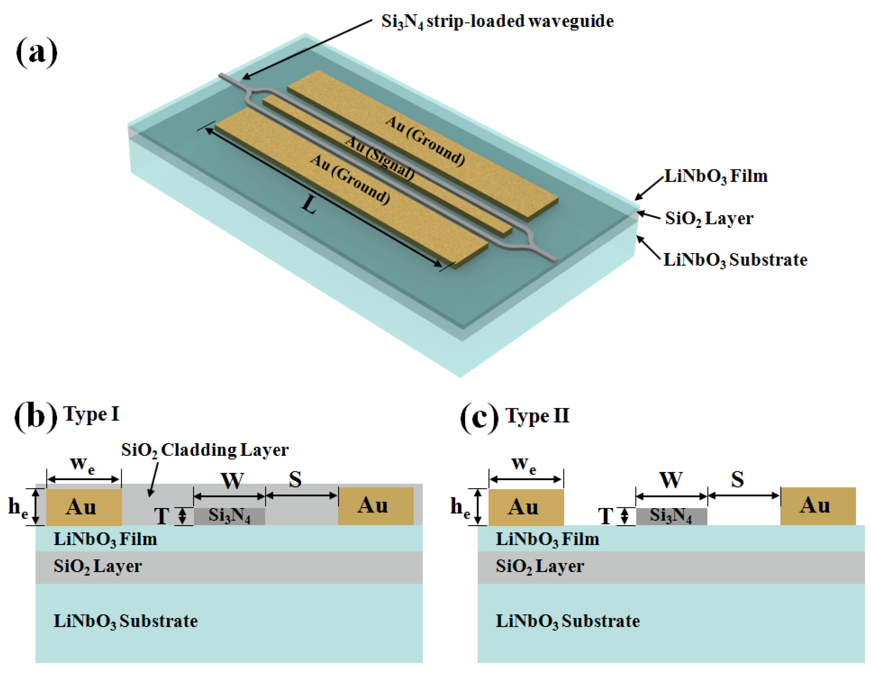
2. Device Description and Methods

The structure of an MZM consists of optical-routing waveguides and coplanar waveguide electrodes. A schematic for this structure is shown in Figure 1a. Two different MZM structures were designed in this research, Type I and Type II, as shown in Figure 1b,c. The LNOI consisted of a 0.5 μm thick x-cut LN thin film bonded to 2 μm thick SiO2 cladding deposited on an LN substrate [2]. The crystal orientation of the LN thin film was chosen to utilize the highest E-O coefficient of LN, r33 = 31 pm/V, at λ = 1.55 µm [22], for the TE mode. To provide lateral optical confinement, a Si3N4-strip-loaded waveguide was located at the top of the LN thin film. Coplanar waveguide electrodes were configured in ground-signal-ground form, and two LN waveguides were located in two gaps between the ground and signal metals. To produce a large E-O modulation bandwidth, the coplanar waveguide electrodes were operated in a traveling wave manner and optimized for impedance matching, as well as velocity matching for the microwave and optical signals. Table 1 shows the refractive indices and dielectric constants of the materials in the simulation at a wavelength of 1.55 µm.
Based on a full-vectorial finite-difference method (FVFDM) [23,24], mode calculation was performed using the commercial software Lumerical: Mode Solutions. The basic principle of the FVFDM was to surround the optical waveguide with a rectangular computing window, discretely dividing the computing window into a grid with equal or unequal spacing, with the selected points on the grid as nodes. The difference quotient of the electric field or magnetic field component of the adjacent node was used to replace the differential quotient of the waveguide equation. In this way, the eigenvalue equation of the matrix could be obtained. By solving the eigenvalue equation, the mode field distribution and the corresponding propagation constant of the eigenmode could be obtained. Based on a finite element method (FEM), the electric field distribution and the RF parameters were simulated using the commercial software COMSOL Multiphysics [25] and a high-frequency structure simulator (HFSS) [26], respectively. The FEM in COMSOL utilized well-known mathematical equations and energy minimization in triangular elements to determine the solutions for the voltage and electric field distributions given specific input models, relevant parameters, and boundary conditions. The principle of the FEM in HFSS was to divide the object into small tetrahedra for calculation, then form a network of all the small tetrahedral elements, and finally obtain the solution of the model using its connection. The HFSS also had an adaptive solution function, which meant that the software analyzed the results and determined the parts with large errors.

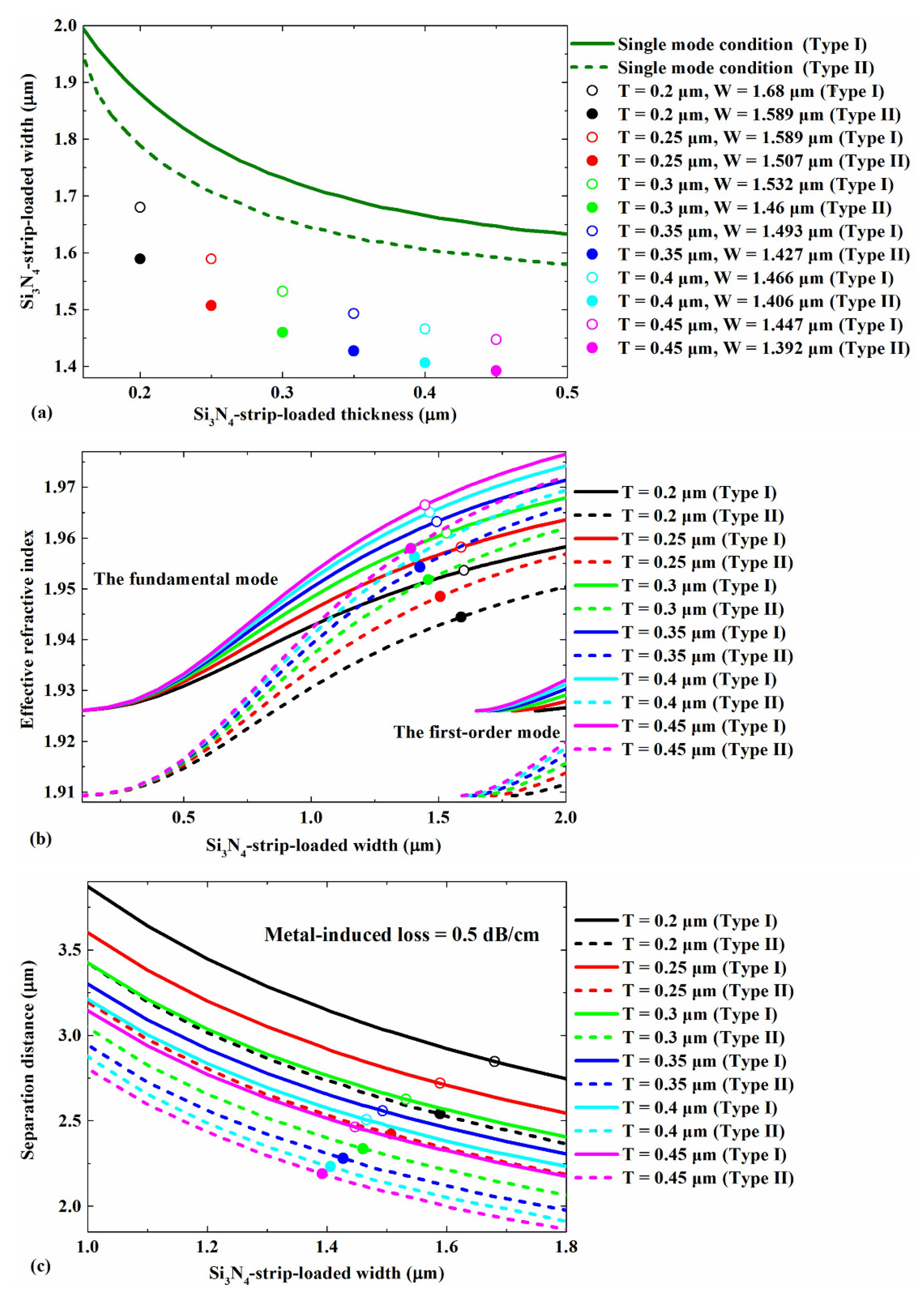
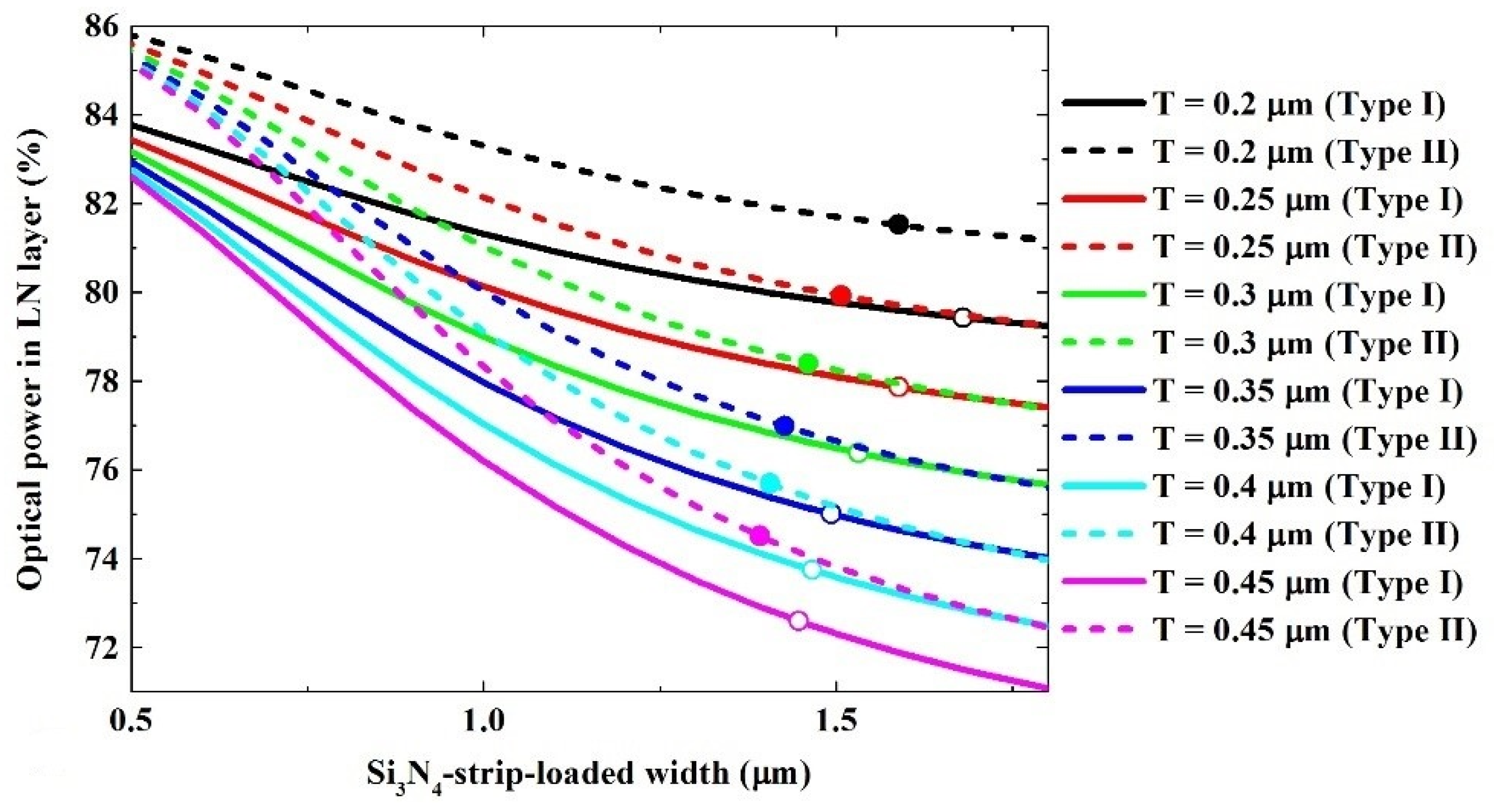
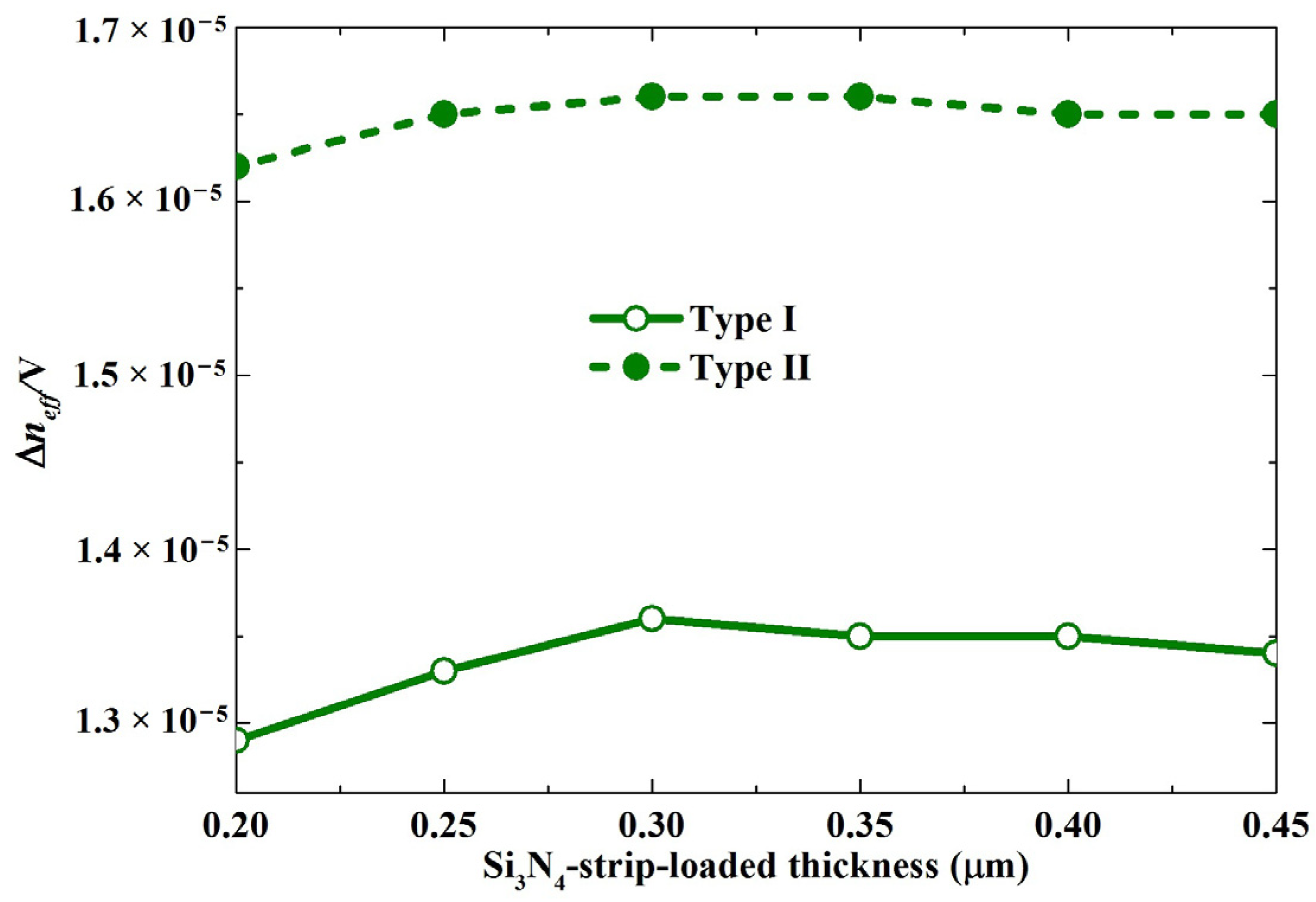
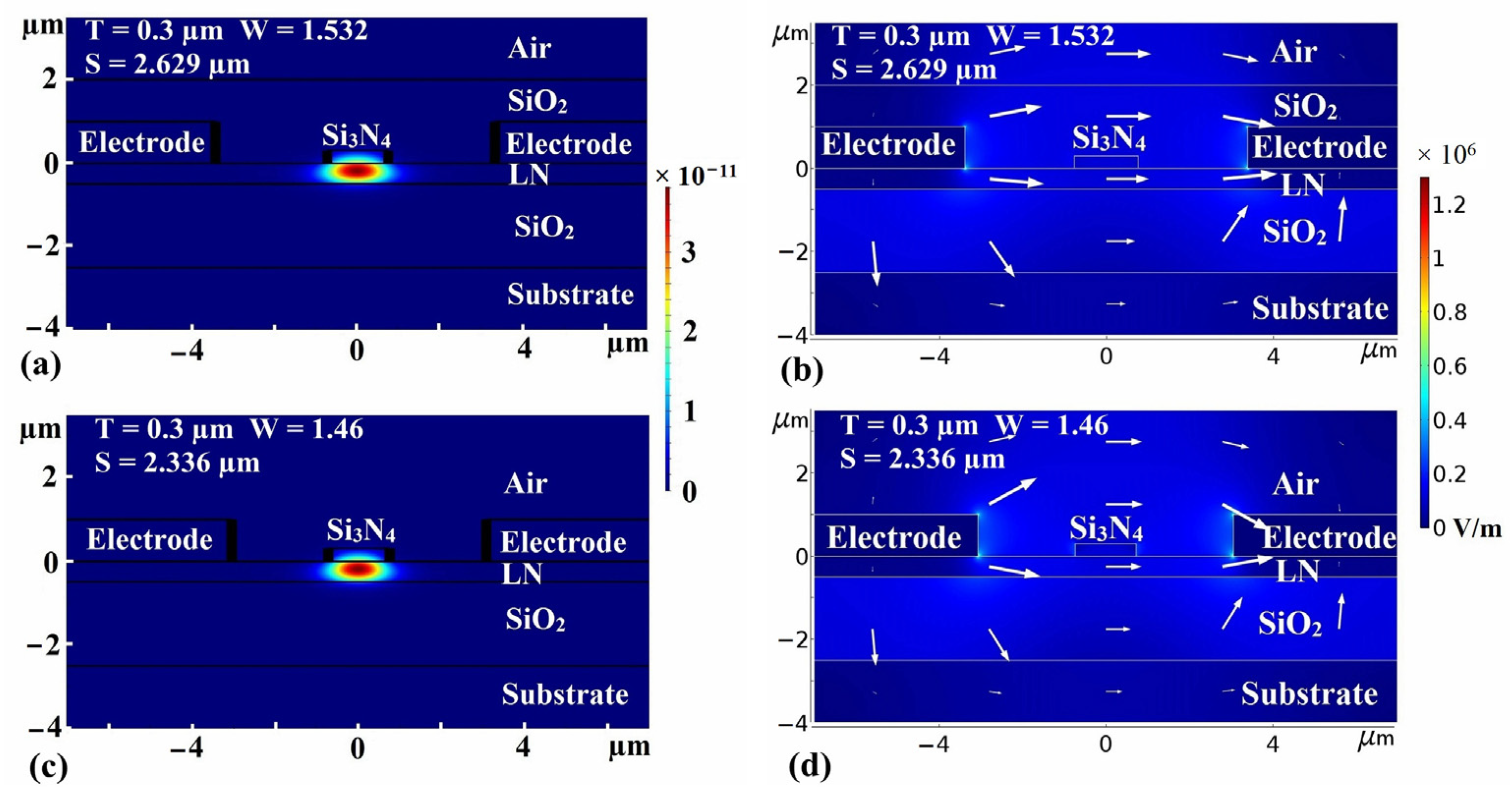
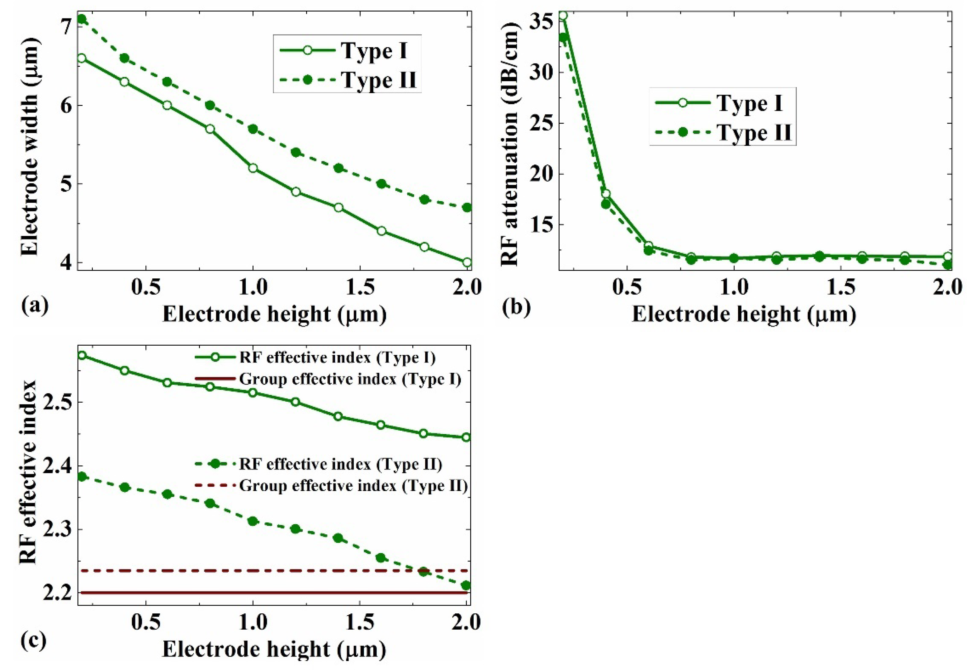
3. Results and Discussion

In this work, we optimized the Si3N4-strip-loaded dimensions based on four aspects: single-mode conditions, the effective refractive index, the separation distance between the electrode edge, and the Si3N4-strip-loaded edge, and the optical power confinement in the LN layer. The single-mode conditions were first investigated because of their advantages: (i) There was no energy transformation between modes. (ii) The signal distortion caused by several modes of transmission at different speeds could be avoided [27]. Figure 2a shows the cutoff dimension of the Si3N4-strip-loaded waveguide for the TE mode between the single- and multi-mode conditions. The cutoff width and thickness of the Si3N4-strip-loaded waveguide for the fundamental mode were both zero. No matter how small the thickness and the width of the Si3N4-strip-loaded waveguide were, there was always a waveguide mode [28]. Waveguides of all widths and thicknesses under the curves satisfied the single-mode conditions. For example, for a 0.3 μm thick Si3N4-strip-loaded Type I, the cutoff width of the achieved single-mode operation was 1.732 μm. The cutoff thickness decreased with the increase in the Si3N4-strip-loaded width. At the same Si3N4-strip-loaded thickness, the cutoff width of Type I was larger than that of Type II. Considering the single-mode conditions, the effective refractive index, and separation distance, six combinations of widths and thicknesses of the Si3N4-strip-loaded waveguide were selected for both the Type I and Type II structures in subsequent simulations, marked in Figure 2 as circles.
The effective refractive indices of the TE fundamental and first-order modes in the Si3N4-strip-loaded waveguides as a function of the width for different thicknesses of the Si3N4-strip-loaded waveguides are presented in Figure 2b. The effective refractive index increased with the increasing width and thickness of the Si3N4-strip-loaded LNOI. At the same Si3N4-strip-loaded width and thickness, the effective refractive index of Type I with the single-mode operation was larger than that of Type II. To ensure that only one electric field intensity peak was supported in the Si3N4-strip-loaded waveguide, the width of the Si3N4-strip-loaded waveguides should be less than the value of the first-order mode. The hollow circles in the figure correspond to the effective refractive index of six combinations of widths and thicknesses of the Si3N4-strip-loaded waveguide for Type I, and the solid circles correspond to the effective refractive index of six combinations of widths and thicknesses of Si3N4-strip-loaded waveguide for Type II.
To obtain a large electric field strength and a low electrode-induced loss in the optical waveguide, an appropriate separation distance between the electrode edge and the Si3N4-strip-loaded edge was selected. The target electrode-induced loss was 0.5 dB/cm in this simulation. The separation distances as a function of the width for different thicknesses of the Si3N4-strip-loaded waveguides are shown in Figure 2c. The separation distance decreased with the increasing width and thickness of the Si3N4-strip-loaded LNOI. At the same Si3N4-strip-loaded width and thickness, the separation distance of Type I was larger than that of Type II. The hollow circles in the figure correspond to the separation distances of the six combinations of widths and thicknesses of the Si3N4-strip-loaded waveguide for Type I, and the solid circles correspond to the separation distance of six combinations of widths and thicknesses of the Si3N4-strip-loaded waveguide for Type II.
The optical power distribution of the Si3N4-strip-loaded LNOI was mainly divided into four parts. The layers from the top to the bottom were the SiO2 layer (Type I) or air layer (Type II), the Si3N4-strip-loaded, the LN layer, and the SiO2 cladding layer. As much optical power as possible is required to be concentrated in the LN layer in E-O applications. Figure 3 shows the optical power in the LN layer, with the thickness and width of the Si3N4-strip-loaded waveguide as the parameters. The optical power in the LN layer decreased with the increasing width and thickness of the Si3N4-strip-loaded waveguide. At the same Si3N4-strip-loaded width and thickness, the optical power in the LN layer of Type I was less than that of Type II. The hollow circles in the figure correspond to the optical power in the LN layer for six combinations of widths and thicknesses of the Si3N4-strip-loaded waveguide for Type I, and the solid circles correspond to the optical power in the LN layer of six combinations of the widths and thicknesses of Si3N4-strip-loaded waveguide for Type II.
Using the distribution of the electrostatic field, the distribution of the refractive index of the LN waveguide was calculated. The effective refractive index change (Δneff) of the TE mode of a single waveguide was the difference between the effective refractive index with and without the voltage. Figure 4 shows the effective refractive index change for six combinations of the Si3N4-strip-loaded widths and thicknesses for the unit voltage. For an increasing Si3N4-strip-loaded thickness and a decreasing Si3N4-strip-loaded width combination, the Δneff/V increased at first but then decreased after reaching the peak at a thickness of 0.3 μm. For the combination of the same thickness of Si3N4-strip-loaded waveguide, the Δneff/V of Type I was smaller than that of Type II. The selection of these parameters was insensitive of Δneff/V.
The single-mode operation, the appropriate optical power in the LN layer, tight waveguide separation, and large Δneff/V enabled an ultra-compact, high-efficiency, and low-loss E-O MZM. Considering the above factors in the subsequent simulations, the thicknesses and widths of the Si3N4-strip-loaded waveguides and the separation distance in Type I and Type II structures are shown in Table 2.
Since the circular arcs in each arm of the structure involved bending waveguides, the relationship between the bending loss and the bending radius is shown in Figure 5. The bending loss decreased exponentially with the bending radius. A small bending radius was necessary for the ultra-compact MZM. The bending losses of Type I was larger than those of Type II. The bending losses of Type I and Type II were both 0.1 dB/cm when the bending radii were 316 and 244 µm.
The distributions of the electric field and the optical mode were simulated. The optical mode distributions of Type I and Type II are shown in Figure 6a,c. Most of the optical power of Type I and Type II was confined within the LN layer. A voltage of 1 V was applied between electrodes. The distribution of the electrostatic field is shown in Figure 6b,d. The electric field intensities in the center of the LN layer below the Si3N4-strip-loaded waveguide for Type I and Type II were 121,103 and 127,997 V/m, respectively. The electric field in the LN layer of Type I was less than that of Type II.
In the E-O MZM (Figure 1), two light beams of equal intensity and phase traveled across two arm waveguides, and finally, the beams combined to form an interference pattern of dark and light fringes. For the two arms, opposite electric fields were applied to modify the refractive index of the LN layer, thus changing the phase of the wave propagating through those arms. The resulting diffraction pattern depended on the difference in the effective refractive index of the two arms. The intensity (I) of the sinusoidal interference signal depended on the interaction length in the optical-modulating waveguide (L) and the change in the effective refractive index Δneff [29,30].
I [ 1 + V cos Δ ϕ ] ,
where Δϕ is the phase shift between the guided modes of the two arms, which is correlated directly to L and Δneff, and V is the change in applied voltage. The phase shift is given by the following equation:
Δ ϕ = 2 π λ Δ n e f f L = V V π π 2 .
where Vπ is the half-wave voltage. For the Type I and Type II devices, when the thickness of the Si3N4-strip-loaded combination was 0.3 µm, the Δneff/V values were 1.36 × 10⁻⁵ and 1.66 × 10⁻⁵ V−1, and the half-wave voltage-length products were calculated as 2.85 and 2.33 V·cm.
HFSS was chosen as the preferred tool for an accurate and high-frequency dependent analysis. HFSS allowed for the geometric definition and analysis of structures in a three-dimensional environment. Perfect electric walls were defined for the signal trace and the ground plane in HFSS. The dielectric was given a permittivity, permeability, and a loss tangent.
The performance of the traveling wave modulator was related to the characteristic impedance of the RF coplanar waveguide electrode, the loss of the RF signal, and the velocity matching of the optical modes and the RF signal. The best modulation efficiency was obtained when the propagation velocity difference between the RF signal and the optical wave was the smallest (velocity-matching condition). This meant that the difference between the RF effective index and the group effective index was smaller [31]. We analyzed the characteristic impedance of the coplanar waveguide electrode structure for different signal electrode dimensions. For each signal electrode thickness, the width of the signal electrode was first adjusted to ensure that the characteristic impedance of the coplanar waveguide electrode was 50 Ω at a frequency of 100 GHz. The relationship between the signal electrode height and width is shown in Figure 7a. A thin signal electrode would require a wide signal electrode to achieve characteristic impedance matching. At the same signal electrode height, the signal electrode width of Type I was smaller than that of Type II because the dielectric constant of SiO2 was larger than that of air. Then, for each combination of the width and height of the signal electrode, the RF effective mode index and the RF attenuation of the electrodes were further analyzed, as shown in Figure 7b,c. For the RF attenuation, thick and narrow signal electrode combination facilitated the low-loss RF signal. When the electrode thickness was larger than 0.8 µm, the decrease in the RF attenuation was saturated, which was also the preferred region for metal thickness in order to achieve the ultimate performance. The group effective indices of the Si3N4-strip-loaded LNOI waveguide for the optical mode are marked in Figure 7c. The group effective index was obviously smaller than the RF effective index for Type I, and the propagation speed of the optical and RF signals was well-matched for Type II. This was because the dielectric constant of the SiO2 was much higher than that of air, so the RF effective index of Type I was significantly higher than that of Type II. In subsequent simulations, considering the RF attenuation and velocity-matching between the RF signal and the optical mode, the signal electrode height was set at 1.8 μm, and the electrode widths for Type I and Type II were set to 4.4 and 4.8 μm, respectively.
The RF electrode–optic frequency response m(ω) could be modeled as [32]:
m ( ω ) = R L + R G R L Z i n Z i n + Z G ( Z L + Z 0 ) F ( u + ) + ( Z L Z 0 ) F ( u ) ( Z L + Z 0 ) e γ m L + ( Z L Z 0 ) e γ m L ,
where RL and RG are the load and generator resistances, respectively. In the expression, Zin is the modulator input impedance:
Z i n = Z 0 Z L + Z 0 tanh ( γ m L ) Z 0 + Z L tanh ( γ m L ) ,
where ZG and ZL are the generator and load impedances, Z0 is the characteristic impedance, F ( u ± ) = ( 1 e u ± ) / u ± , where u ± = ± α m L + j ω ( ± n m n g ) L / c 0 , and γ m = α m + j ω n m / c 0 is the propagation constant. In this expression, nm and αm are the RF effective mode index and RF attenuation. The units of αm are Np/cm, with 1 Np/cm equal to 8.68 dB/cm. c0 is the speed of light in a vacuum. We assumed RL = RG = ZG = ZL = 50 Ω.
The overall modulation frequency response of a traveling wave modulator could be calculated with the characteristic impedance, RF attenuation, RF effective index, and group effective index [30,33]. Figure 8a shows the characteristic impedance of the MZM at frequencies in the range of 0–1.3 THz. The characteristic impedance curves of Type I and Type II were highly coincident, ranging from 47.5 Ω to 56 Ω. Figure 8b shows the RF attenuation. At frequencies from 0 to 1.3 THz, the RF attenuation curves of Type I and Type II were very similar, ranging from 4 dB/cm to 47 dB/cm. Figure 8c shows the RF effective index at frequencies in the range of 0–1.3 THz. The group effective indices of the optical mode are marked in Figure 8c for comparison. For the Type I device, the group effective index was always obviously smaller than the RF effective index at the frequencies in the range of 0–1.3 THz. For the Type II device, the group effective index was smaller than the RF effective index at the frequencies in the range of 0–0.1 THz, but the propagation speed of the optical and RF signals was well-matched at the frequencies in the range of 0.1–1.3 THz. Figure 8d shows the E-O frequency response at the frequencies in the range of 0–1.3 THz. The modeled bandwidths (−3 dB) with the interaction lengths of 3, 5, and 10 mm for Type I were 0.083, 0.214, and 0.4 THz, and those for Type II were 0.23, 0.79, and 1.26 THz, respectively.
Table 3 shows the comparison of the performance of the present device with state-of-the-art devices, including the interaction length, half-wave voltage length product, −3 dB E-O bandwidth, and waveguide width. The E-O bandwidth of the Type II device with a length of 3 mm extended to 1200 GHz, the highest bandwidth for an LN modulator.

4. Conclusions

We demonstrated an E-O MZM configuration with high-performance modulation in a Si3N4-strip-loaded 0.5 μm thick x-cut LNOI. The widths and thicknesses of the Si3N4-strip-loaded waveguides of Type I and Type II were optimized. The optimized values of Vπ·L for Type I and Type II were calculated to be 2.85 and 2.33 V·cm, respectively. The widths and heights of the coplanar waveguide electrodes for Type I and Type II were optimized. The −3 dB E-O modulation bandwidths for Type I and Type II with a device length of 3 mm were calculated to be 0.4 and 1.26 THz, respectively. The process of this design, which did not require etching or sawing of LN, was based on a current silicon nitride ultra-low-loss passive optical waveguide.

Author Contributions

Conceptualization, H.H. and B.X.; methodology, H.H.; software, H.H. and B.X.; validation, H.H., F.Y., C.L., Z.W., Y.J., G.C.; S.R., and B.X.; formal analysis, S.R. and B.X.; investigation, H.H. and B.X.; resources, B.X.; data curation, B.X.; writing—original draft preparation, H.H.; writing—review and editing, H.H. and B.X.; visualization, H.H.; supervision, B.X.; project administration, B.X.; funding acquisition, B.X. All authors have read and agreed to the published version of the manuscript.

Funding

This research was funded by the National Natural Science Foundation of China, grant numbers 12105190 and 61935014; and Shenzhen Science and Technology Planning, grant number JCYJ20190813103207106 to H.H and B.X.

Institutional Review Board Statement

Not applicable.

Informed Consent Statement

Not applicable.

Data Availability Statement

Not applicable.

Conflicts of Interest

The authors declare no conflict of interest.

References

  1. Poberaj, G.; Hu, H.; Sohler, W.; Günter, P. Lithium niobate on insulator (LNOI) for micro-photonic devices. Laser Photonics Rev. 2012, 6, 488–503. [Google Scholar] [CrossRef]
  2. Han, H.; Cai, L.; Hu, H. Optical and structural properties of Single-crystal lithium niobate thin film. Opt. Mater. 2015, 42, 47–51. [Google Scholar] [CrossRef]
  3. Wang, C.; Zhang, M.; Chen, X.; Bertrand, M.; Shams-Ansari, A.; Chandrasekhar, S.; Winzer, P.; Lončar, M. Integrated lithium niobate electro-optic modulators operating at CMOS-compatible voltages. Nature 2018, 562, 101–104. [Google Scholar] [CrossRef] [PubMed]
  4. Xu, M.; He, M.; Zhang, H.; Jian, J.; Pan, Y.; Liu, X.; Chen, L.; Meng, X.; Chen, H.; Li, Z.; et al. High-performance coherent optical modulators based on thin-film lithium niobate platform. Nat. Commun. 2020, 11, 3911. [Google Scholar] [CrossRef] [PubMed]
  5. Hu, H.; Ricken, R.; Sohler, W. Lithium niobate photonic wires. Opt. Express 2009, 17, 24261–24268. [Google Scholar] [CrossRef]
  6. Krasnokutska, I.; Tambasco, J.-L.J.; Li, X.; Peruzzo, A. Ultra-low loss photonic circuits in Lithium Niobate on Insulator. Opt. Express 2017, 26, 897–904. [Google Scholar] [CrossRef] [Green Version]
  7. Guarino, A.; Poberaj, G.; Rezzonico, D.; Degl’innocenti, R.; Günter, P. Electro-optically tunable microring resonators in lithium niobate. Nat. Photon. 2007, 1, 407–410. [Google Scholar] [CrossRef]
  8. Ahmed, A.N.R.; Shi, S.; Zablocki, M.; Yao, P.; Prather, D.W. Tunable hybrid silicon nitride and thin-film lithium niobate electro-optic microresonator. Opt. Lett. 2019, 44, 618–621. [Google Scholar] [CrossRef] [Green Version]
  9. Ahmed, A.N.R.; Nelan, S.; Shi, S.; Yao, P.; Mercante, A.; Prather, D.W. Subvolt electro-optical modulator on thin-film lithium niobate and silicon nitride hybrid platform. Opt. Lett. 2020, 45, 1112–1115. [Google Scholar] [CrossRef]
  10. Jin, S.; Xu, L.; Zhang, H.; Li, Y. LiNbO3 thin-film modulators using silicon nitride surface ridge waveguides. IEEE Photonics Technol. Lett. 2016, 28, 736–739. [Google Scholar] [CrossRef]
  11. Liu, D.; Feng, L.; Jia, Y.; Ma, H. Heterogeneous integration of LN and Si3N4 waveguides using an optical interlayer coupler. Opt. Commun. 2018, 436, 1–6. [Google Scholar] [CrossRef]
  12. Ahmed, A.N.R.; Mercante, A.; Shi, S.; Yao, P.; Prather, D.W. Vertical mode transition in hybrid lithium niobate and silicon nitride-based photonic integrated circuit structures. Opt. Lett. 2018, 43, 4140–4143. [Google Scholar] [CrossRef] [Green Version]
  13. Qiu, W.; Bernal, M.P.; Ndao, A.; Guyot, C.; Hameed, N.M.; Courjal, N.; Maillotte, H.; Baida, F.I. Analysis of ultra-compact waveguide modes in thin film lithium niobate. Appl. Phys. B 2015, 118, 261–267. [Google Scholar] [CrossRef]
  14. Wang, Y.; Chen, Z.; Hu, H. Analysis of waveguides on lithium niobate thin films. Crystals 2018, 8, 191. [Google Scholar] [CrossRef] [Green Version]
  15. Sarma, A.K.; Saha, M.; Biswas, A. Effect of two-photon absorption on soliton propagation and soliton-soliton interaction in a silicon waveguide. Opt. Eng. 2010, 49, 211–223. [Google Scholar] [CrossRef]
  16. Cao, L.; Aboketaf, A.; Wang, Z.; Preble, S. Hybrid amorphous silicon (a-Si:H)–LiNbO3 electro-optic modulator. Opt. Commun. 2014, 330, 40–44. [Google Scholar] [CrossRef]
  17. Chiles, J.; Fathpour, S. Mid-infrared integrated waveguide modulators based on silicon-on-lithium-niobate photonics. Optica 2014, 1, 350–355. [Google Scholar] [CrossRef]
  18. Rao, A.; Malinowski, M.; Honardoost, A.; Talukder, J.R.; Rabiei, P.; Delfyett, P.; Fathpour, S. Secondharmonic generation in periodically-poled thin film lithium niobate wafer-bonded on silicon. Opt. Express 2016, 24, 29941–29947. [Google Scholar] [CrossRef] [Green Version]
  19. Chang, L.; Pfeiffer, M.H.P.; Volet, N.; Zervas, M.; Peters, J.D.; Manganelli, C.L.; Stanton, E.J.; Li, Y.; Kippenberg, T.J.; Bowers, J.E. Heterogeneous integration of lithium niobate and silicon nitride waveguides for wafer-scale photonic integrated circuits on silicon. Opt. Lett. 2017, 42, 803–806. [Google Scholar] [CrossRef]
  20. Boes, A.; Corcoran, B.; Chang, L.; Bowers, J.; Mitchell, A. Status and potential of lithium niobate on insulator (LNOI) for photonic integrated circuits. Laser Photonics Rev. 2018, 12, 1700256. [Google Scholar] [CrossRef]
  21. Huffman, T.; Brodnik, G.M.; Pinho, C.; Gundavarapu, S.; Baney, D.; Blumenthal, D.J. Integrated resonators in ultra-Low loss Si3N4/SiO2 for multifunction applications. IEEE J. Sel. Top. Quant. 2018, 24, 1. [Google Scholar] [CrossRef]
  22. Wong, K.K. Properties of Lithium Niobate, 1st ed.; INSPEC: London, UK, 2002; pp. 115–128. [Google Scholar]
  23. Dai, D.; Zhen, S. Numerical analysis of silicon-on-insulator ridge nanowires by using a full-vectorial finite-difference method mode solver. J. Opt. Soc. Am. B 2007, 24, 2853–2859. [Google Scholar] [CrossRef]
  24. Zhu, Z.; Brown, T.G. Full-vectorial finite-difference analysis of microstructure optical fibers. Opt. Express 2002, 10, 853–864. [Google Scholar] [CrossRef] [PubMed]
  25. Afrouzi, H.N.; Abdul-Malek, Z.; Mashak, S.V.; Naderipour, A. Three-dimensional potential and electric field distributions in hv cable insulation containing multiple cavities. Adv. Mat. Res. 2014, 845, 372–377. [Google Scholar]
  26. Rahman, B.; Fernandez, F.A. Review of finite element methods for microwave and optical waveguides. Proc. IEEE 1991, 79, 1442–1448. [Google Scholar] [CrossRef]
  27. Lvescan, S.; Vonsovici, A. The single-mode condition for semiconductor rib waveguides with large cross section. J. Lightwave Technol. 1998, 16, 1851–1853. [Google Scholar]
  28. Uchida, N. Optical waveguide loaded with high refractive-index strip film. Appl. Opt. 1976, 15, 179–182. [Google Scholar] [CrossRef]
  29. Sieger, M.; Balluff, F.; Wang, X.; Kim, S.S.; Leidner, L.; Gauglitz, G.; Mizaikoff, B. On-chip integrated mid-infrared GaAs/AlGaAs Mach-Zehnder interferometer. Anal. Chem. 2013, 85, 3050–3052. [Google Scholar] [CrossRef]
  30. Wang, J.; Xu, S.; Chen, J.; Zou, W. A heterogeneous silicon on lithium niobate modulator for ultra-compact and high-performance photonic integrated circuits. IEEE Photonics J. 2021, 1, 99. [Google Scholar] [CrossRef]
  31. García-Granda, M.; Hu, H.; Rodríguez-García, J.; Sohler, W. Design and fabrication of novel ridge guide modulators in lithium niobate. J. Lightwave Technol. 2010, 27, 5690–5697. [Google Scholar] [CrossRef]
  32. Ghion, G. Semiconductor Devices for High-Speed Optoelectronics, 1st ed.; Cambridge University: New York, NY, USA, 2009; pp. 375–391. [Google Scholar]
  33. He, M.; Xu, M.; Ren, Y.; Jian, J.; Ruan, Z.; Xu, Y.; Gao, S.; Sun, S.; Wen, X.; Zhou, L.; et al. High-performance hybrid silicon and lithium niobate Mach–Zehnder modulators for 100 Gbit s−1 and beyond. Nat. Photonics 2019, 13, 359–364. [Google Scholar] [CrossRef]
  34. Rao, A.; Patil, A.; Rabiei, P.; Honardoost, A.; Desalvo, R.; Paolella, A.; Fathpour, S. High-performance and linear thin-film lithium niobate Mach–Zehnder modulators on silicon up to 50 GHz. Opt. Lett. 2016, 41, 5700–5703. [Google Scholar] [CrossRef] [PubMed]
  35. Zhang, P.; Huang, H.; Jiang, Y.; Han, X.; Xiao, H.; Frigg, A.; Nguyen, T.G.; Boes, A.; Ren, G.; Su, Y.; et al. High-speed electro-optic modulator based on silicon nitride loaded lithium niobate on an insulator platform. Opt. Lett. 2021, 46, 5986–5989. [Google Scholar] [CrossRef] [PubMed]
  36. Honardoost, A.; Juneghani, F.A.; Safian, R.; Fathpour, S. Towards subterahertz bandwidth ultracompact lithium niobate electrooptic modulators. Opt. Express 2019, 27, 6495–6501. [Google Scholar] [CrossRef]
  37. Boynton, N.; Cai, H.; Gehl, M.; Arterburn, S.; Dallo, C.; Pomerene, A.; Starbuck, A.; Hood, D.; Trotter, D.C.; Friedmann, T.; et al. A heterogeneously integrated silicon photonic/lithium niobate travelling wave electro-optic modulator. Opt. Express 2020, 28, 1868–1884. [Google Scholar] [CrossRef] [PubMed]
  38. Weigel, P.O.; Zhao, J.; Fang, K.; Al-Rubaye, H.; Trotter, D.; Hood, D.; Mudrick, J.; Dallo, C.; Pomerene, A.T.; Starbuck, A.L.; et al. Bonded thin film lithium niobate modulator on a silicon photonics platform exceeding 100 GHz 3-dB electrical modulation bandwidth. Opt. Express 2018, 26, 23728–23739. [Google Scholar] [CrossRef] [PubMed] [Green Version]
Figure 1. (a) Schematic of the Si3N4-strip-loaded MZM in LNOI. The cross-section schematics of the MZMs of (b) Type I (packaged with 2 µm thick SiO2) and (c) Type II (unpackaged).
Photonics 09 00500 g001
Figure 2. (a) Cutoff dimensions for TE mode between the single- and multi-mode conditions; (b) effective indices of the TE fundamental mode and (c) separation distance between the electrode edge and the Si3N4-strip-loaded edge as a function of the width for different thicknesses of the Si3N4-strip-loaded waveguides. The modes were calculated at λ = 1.55 µm.
Photonics 09 00500 g002
Figure 3. Optical power distributions in the LN layer of the TE fundamental mode as a function of width for different Si3N4-strip-loaded thicknesses. The modes were calculated at λ = 1.55 µm.
Photonics 09 00500 g003
Figure 4. Effective refractive index change for six combinations of the Si3N4-strip-loaded widths and thicknesses for unit voltage. The modes were calculated at λ = 1.55 µm.
Photonics 09 00500 g004
Figure 5. Dependence of the bending loss on the radius of the bending waveguide. The modes were calculated at λ = 1.55 µm.
Photonics 09 00500 g005
Figure 6. Optical field distribution of (a) Type I and (c) Type II. Electrostatic field distribution of (b) Type I and (d) Type II after a 1 V voltage was applied to the electrodes.
Photonics 09 00500 g006
Figure 7. The relationship between the signal electrode height and (a) width, (b) RF attenuation, and (c) RF effective mode index of the coplanar waveguide electrode. The real part of the characteristic impedance was kept at 50 Ω.
Photonics 09 00500 g007
Figure 8. (a) Characteristic impedance, (b) RF attenuation, (c) RF effective mode index nm, and (d) modulation response variation as RF frequency.
Photonics 09 00500 g008
Table 1. Refractive indices (λ = 1.55 µm) and dielectric constants of the materials in simulation.
MaterialRefractive IndexDielectric Constant
Ordinary Refractive
Index (no)
Extraordinary
Refractive Index (ne)
LN [22]2.2112.13828.4
SiO21.4453.9
Si3N41.9897.5
Table 2. The parameters of the dimensions of the Si3N4-strip-loaded waveguides and the separation distance.
TypeThickness (µm)Width (µm)Separation Distance (µm)
Type I0.31.5322.629
Type II0.31.462.336
Table 3. Comparison of the modulator performance of LNOI-based modulator.
StructureExperimental
or Theoretical
Interaction
Length (mm)
Vπ·L
(V·cm)
Bandwidth
(GHz)
References
SiNx-LNOIExperimental1238[10]
SiN-LNOIExperimental83.133[34]
Si3N4-LNOIExperimental7.82.2480[35]
SiN-LNOITheoretical33.6420[36]
LNOI-SiNxExperimental56.6730.6[37]
LN ridgeExperimental102.380[3]
LN ridgeExperimental32.2>70[33]
Si-LNOIExperimental56.7>100[38]
Si-LNOITheoretical51.76350[30]
Si3N4-LNOI (Type I)Theoretical32.85400This work
Si3N4-LNOI (Type I)Theoretical102.8583This work
Si3N4-LNOI (Type II)Theoretical32.331260This work
Si3N4-LNOI (Type II) 102.33230This work
Publisher’s Note: MDPI stays neutral with regard to jurisdictional claims in published maps and institutional affiliations.

