Article

Low-Cost 3D-Printed Electromagnetically Driven Large-Area 1-DOF Optical Scanners

1
Graduate Institute of Photonics and Optoelectronics, National Taiwan University, Taipei 10617, Taiwan
2
Department of Electrical Engineering, National Taiwan University, Taipei 10617, Taiwan
*
Author to whom correspondence should be addressed.
Photonics 2022, 9(7), 484; https://doi.org/10.3390/photonics9070484
Submission received: 13 May 2022 / Revised: 5 July 2022 / Accepted: 6 July 2022 / Published: 11 July 2022

Abstract

:
In this paper, we demonstrate 3D-printed 1-DOF (one torsional axis; 1 degree of freedom) optical scanners with large mirror areas (up to 20 × 20 mm2). Each device consists of an aluminum-coated square silicon substrate serving as the mirror, two miniature permanent magnets, an electromagnet, and a 3D-printed structure including the mirror frame, torsion springs, and base. One device can reach a static half optical scan angle of 14.8 deg., i.e., a full optical scan angle of 29.6 deg., at 12 VDC; this particular device exhibits a mechanical resonance frequency of 84 Hz. These scanners can be a potential, low-cost alternative to the expensive conventional galvanometer scanners.

1. Introduction

Optical scanners have been frequently found in various types of optical systems. Among them, the galvanometer scanners [1,2] are perhaps most popular thanks to their commercial availability and reasonable pricing; outstanding efforts have also been put into analyzing and optimizing the scanning functions [2,3]. They can be found widely in the market [4,5,6]. Their sizes fall within the range from a few millimeters to a few centimeters. Some of them can even reach an optical scan angle of 40 degrees [4]. They are commonly seen in early optical coherence tomography (OCT) systems, either to direct the light beam to the sample [7], or to generate the necessary optical pathlength difference for depth scanning [8]. Other applications include laser scanning microscopy, LiDAR, etc. [9,10]. Although affordable, the cost ranges from a few thousand US dollars to more than ten US dollars [5]; therefore, galvanometer scanners are usually not considered as a low-cost option. Particularly, at the developing phase of a system or experiment that involves galvanometer scanners, the required specifications of the scanners may still be unclear. The price tags of the galvanometer scanners prevent researchers from moving rapidly forwards for a practical trial; contrarily, they spend much effort carefully designing “on paper” in advance just to make sure they get the right scanners later for their systems. This philosophy exists in most research groups in academia and industry, and somewhat slow down the technology development progress.
Riding on the shoulders of the MEMS fabrication technologies, various MEMS optical scanners have been developed. The common driving mechanisms of MEMS scanners include electrostatic actuation [11,12], electromagnetic actuation [13,14], electrothermal actuation [15,16], and piezoelectric actuation [17]. Many electrostatic micromirrors require undesirable high voltages that sometimes approach a hundred volts [18]; electrothermal actuation and electromagnetic actuation both lead to direct heating of the mirror, which can potentially change the mirror parameters such as the curvature; piezoelectric material is less popular in semiconductor fabrication business. Despite these shortcomings, MEMS scanners (mostly micromirrors) make it feasible to accomplish system miniaturization and portability. The fabrication normally requires cleanroom usage and the extremely expensive and heavy equipment such as the etching and deposition machines. Their costs can be lowered by using wafer-level fabrication processes for mass production. However, this is only possible with mature products of high demand; in other words, academia or business developing new products mostly still suffers the high cost per device resulting from the cleanroom microfabrication process. Moreover, the typical sizes of MEMS scanners are between a few hundred microns and a few millimeters, which makes them unsuitable for handling light beams with large cross sections; this limits the number of resolvable spots [19] in a laser scanning system such as the laser scanning microscope and laser scanning projector.
Prism scanners belong to another category which has drawn a great deal of attention [20,21,22]. Distinct from mirrors, prims are transparent optical components whereby the light paths do not need to be folded, making it easier to design and construct the optical systems. Beautiful scan patterns were previously presented using rotational Risley prisms [20]. The only concern about prism scanners is the prisms’ bulky sizes, which make fast scanning somewhat challenging.
In this paper, we demonstrate 3D-printed optical scanners with large mirror areas (up to 20 × 20 mm2). The main mechanical structure of the device is fabricated by FDM (fused deposition modeling) 3D printing; an aluminum-coated silicon chip is mounted on the top to serve as the reflecting surface. Each scanner is equipped with miniature permanent magnets and driven by an electromagnet; both the permanent magnets and electromagnet are off the shelf with extremely low prices. No electric current is delivered to the mirror so there is no issue of heating the mirror. The devices presented in this paper exhibit low driving voltages and are positioned to be an extremely low-cost alternative to the expensive conventional galvanometer scanners. The estimated cost per device is less than ten US dollars. Furthermore, thanks to the rapid prototyping of 3D printing, the turnaround time to complete fabrication and delivery is <1 week.

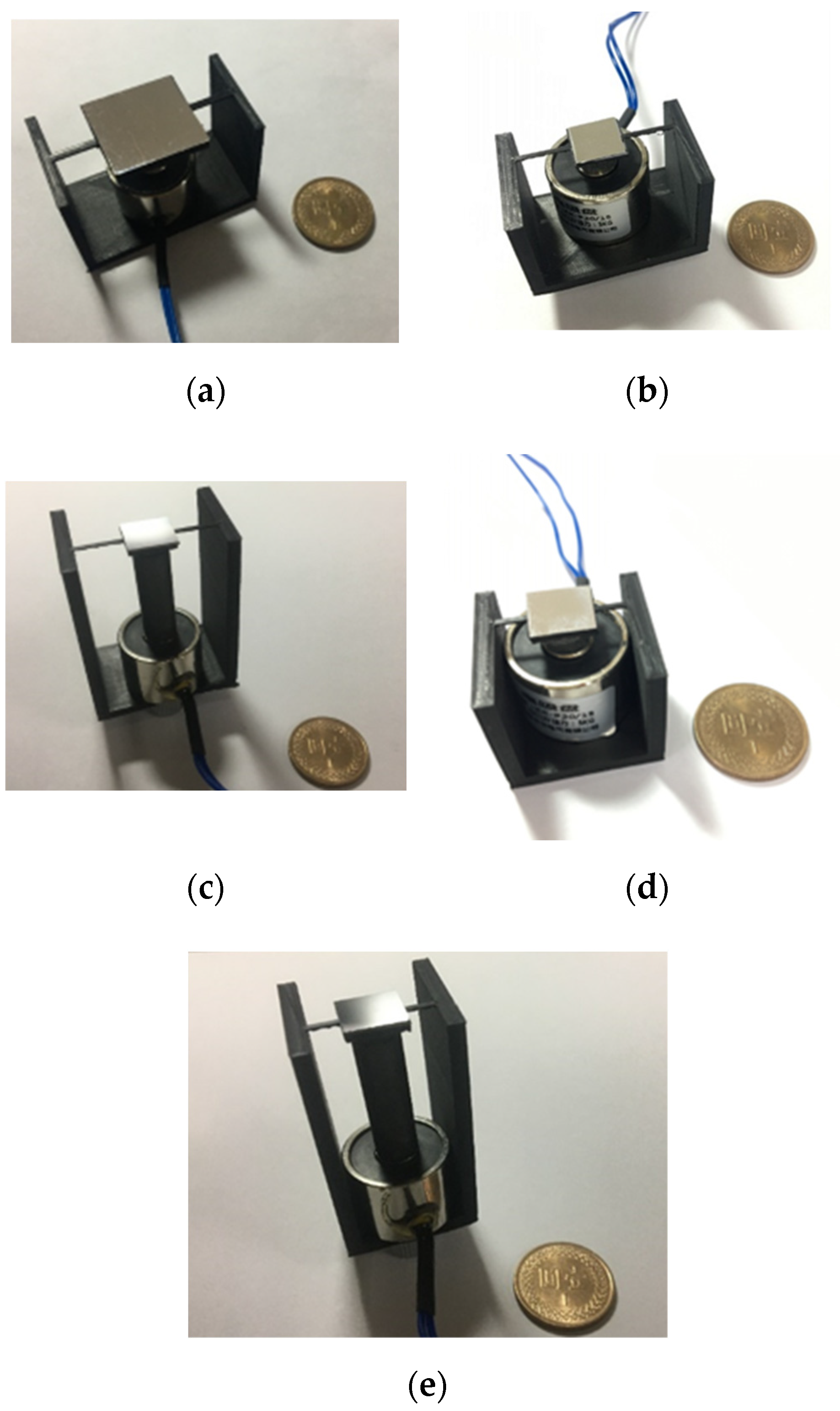
2. Device Design and Fabrication

We propose using FDM (fused deposition modeling) 3D printing to fabricate our devices. FDM 3D printing possesses the advantages of low cost, high speed, and large area printing. Compared to other printing techniques such as stereolithography (SLA) 3D printing and selective laser sintering (SLS) 3D printing, it is more environment-friendly because it avoids the use of the photocurable resin and polymer powder. The printed material is polylactic acid (PLA), which is low-cost and environment-friendly; the printer used in this study is Ultimaker 2+.
Each device consists of an aluminum-coated square silicon substrate serving as the mirror, two miniature permanent magnets, an electromagnet, and a 3D-printed structure including the mirror frame, torsion springs, and base; if needed, a soft iron core can be used to extend the magnetic field produced by the electromagnet. As shown in Figure 1, the exploded view drawing of the device, the two miniature permanent magnets are attached beneath the mirror frame, oriented in opposite directions. When an electric current is sent through the electromagnet, attracting and repelling forces and, therefore, a torque are generated to rotate the mirror. The magnetic flux density generated by the electromagnet is 200 G at 5 V.
The two practical arrangements are shown in Figure 2, one without the soft iron core for extension (type I) and the other with it (type II). For type I devices, the electromagnet generates a magnetic field to directly attract or repel the miniature permanent magnets (oriented in opposite directions) under the mirror frame to drive the mirror to rotate. For type II devices, a soft iron core is connected to the electromagnet to make the magnetic field extend upward along the soft iron core. In this way, the distance between the electromagnet and the miniature permanent magnets can be increased.
The main structure of the device is made by FDM 3D printing. An aluminum-coated silicon chip (slice) is mounted on the frame to serve as the mirror. Then, the miniature permanent magnets are attached to the back of the mirror frame, and the electromagnet is placed on the base.
In our study, five different designs are employed. Their schematic 3D drawings (not to scale) and designed dimensions can be found in Table 1. Table 2 summarizes the specifications of all of the designs. Figure 3 shows the photos of the actual fabricated devices.

3. Device Characterization and Results

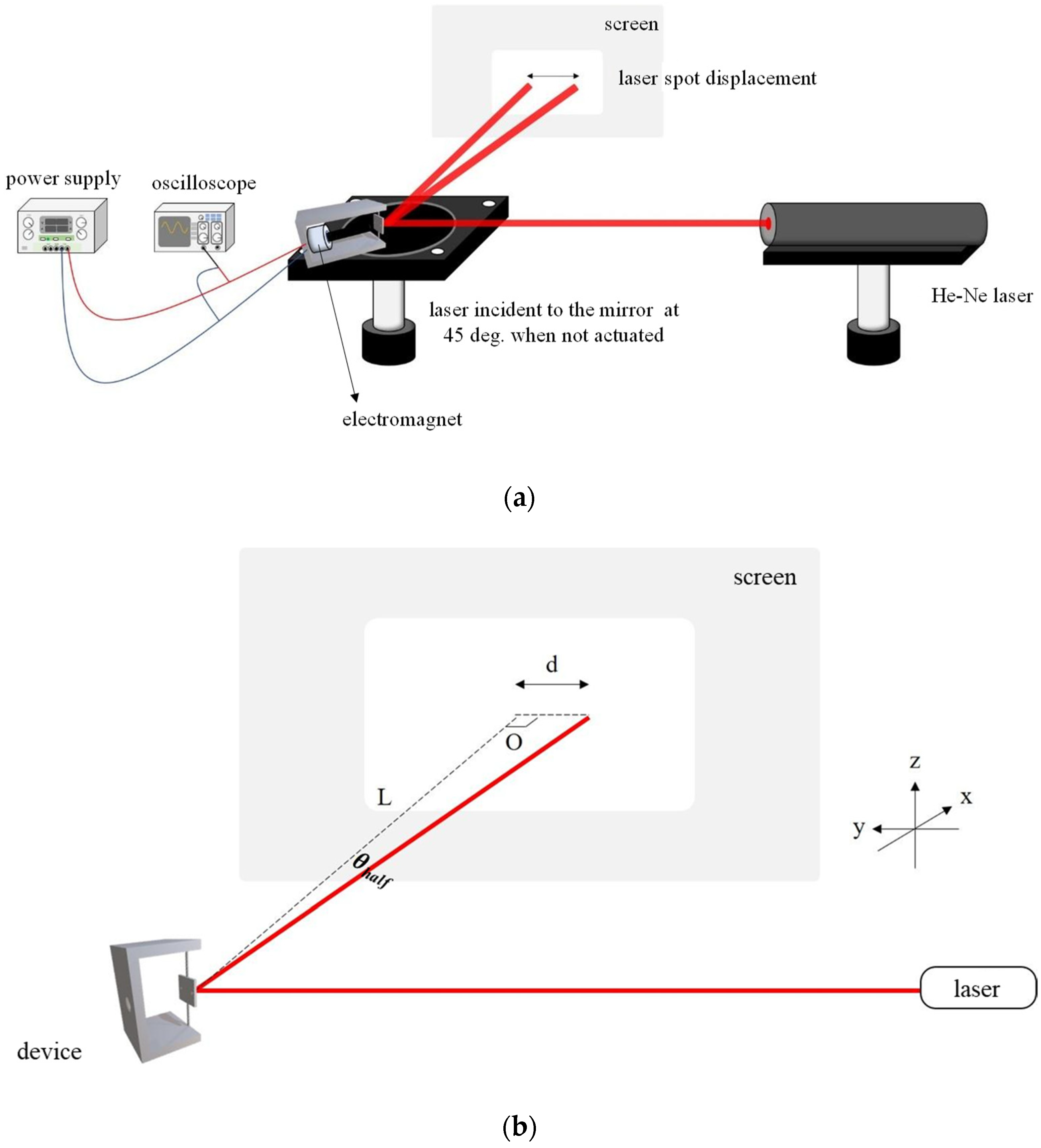
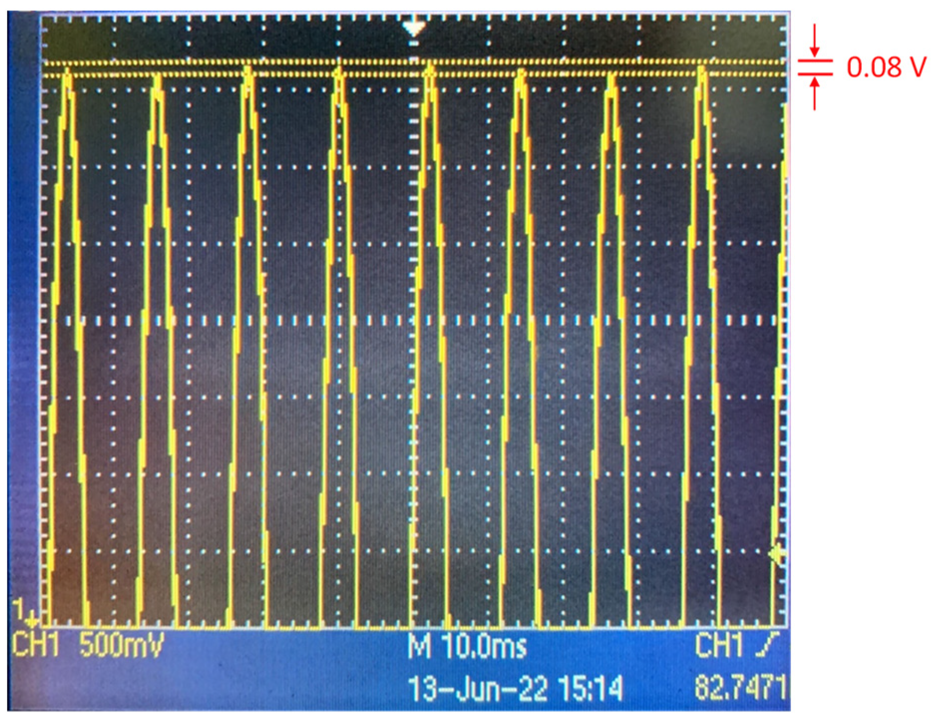
3.1. Experiment Setup and Characterization

The device characterization mainly focuses on measuring the scan angles of all of the designs. Specifically, for each design we will experimentally find out the static optical deflection angles at different applied dc voltages, i.e., the dc characteristic. The scanner will also be driven with a sinusoidal voltage for dynamic characterization; the frequency of the sinusoidal waveform will be tuned and the scan range at each frequency will be recorded; this measurement can lead to the discovery of the frequency response and resonance frequency.
Figure 4a is the schematic drawing of the experimental setup used to obtain the dc characteristic. A 632.8 nm HeNe laser is incident on the mirror and reflected toward a screen. The power supply provides a dc voltage which is applied to the electromagnet while the oscilloscope measures the exact voltage drop across the electromagnet. When the voltage is tuned, the reflected laser spot on the screen moves and the displacement d is recorded. As shown in Figure 4b, given the distance L between the scanner and screen, the optical deflection angle at a certain voltage is then tan−1(d/L), which is considered as the optical half angle θhalf. Flipping the voltage polarity overturns the polarity of the electromagnet, and rotates the mirror toward the opposite direction; therefore, in the ideal case the full scan range of the scanner is twice the maximum optical half angle, i.e., 2θhalf, max.
The measurement setup for dynamic characterization is similar to that for dc characterization, as shown in Figure 5a, with the replacement of the power supply by a function generator. With a sinusoidal voltage applied to the electromagnet, the electromagnet’s polarity flips periodically; this enables the mirror to swing to the two extremes alternately. As shown in Figure 5b, θfull = 2 θhalf = 2tan−1(d/2L) is the full optical scan range at a certain voltage amplitude and frequency. To find the frequency response of the device, the frequency of the sinusoidal waveform is swept manually while keeping the amplitude across the electromagnet constant, and the full optical scan ranges at several frequencies are recorded.

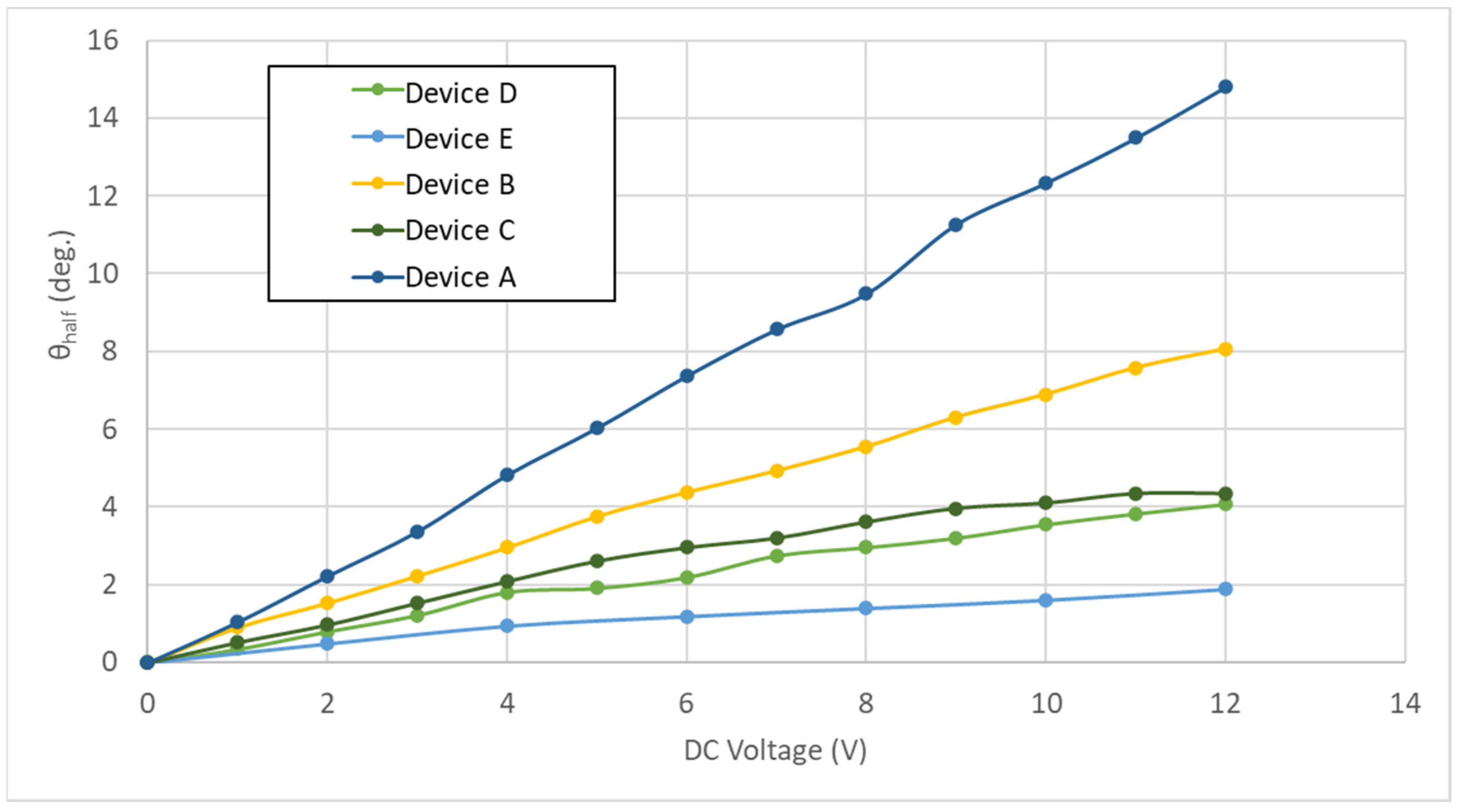
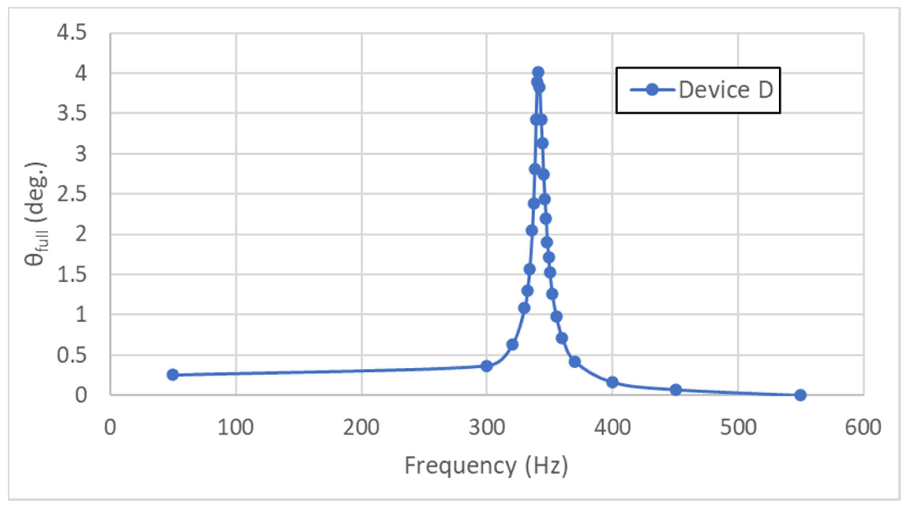
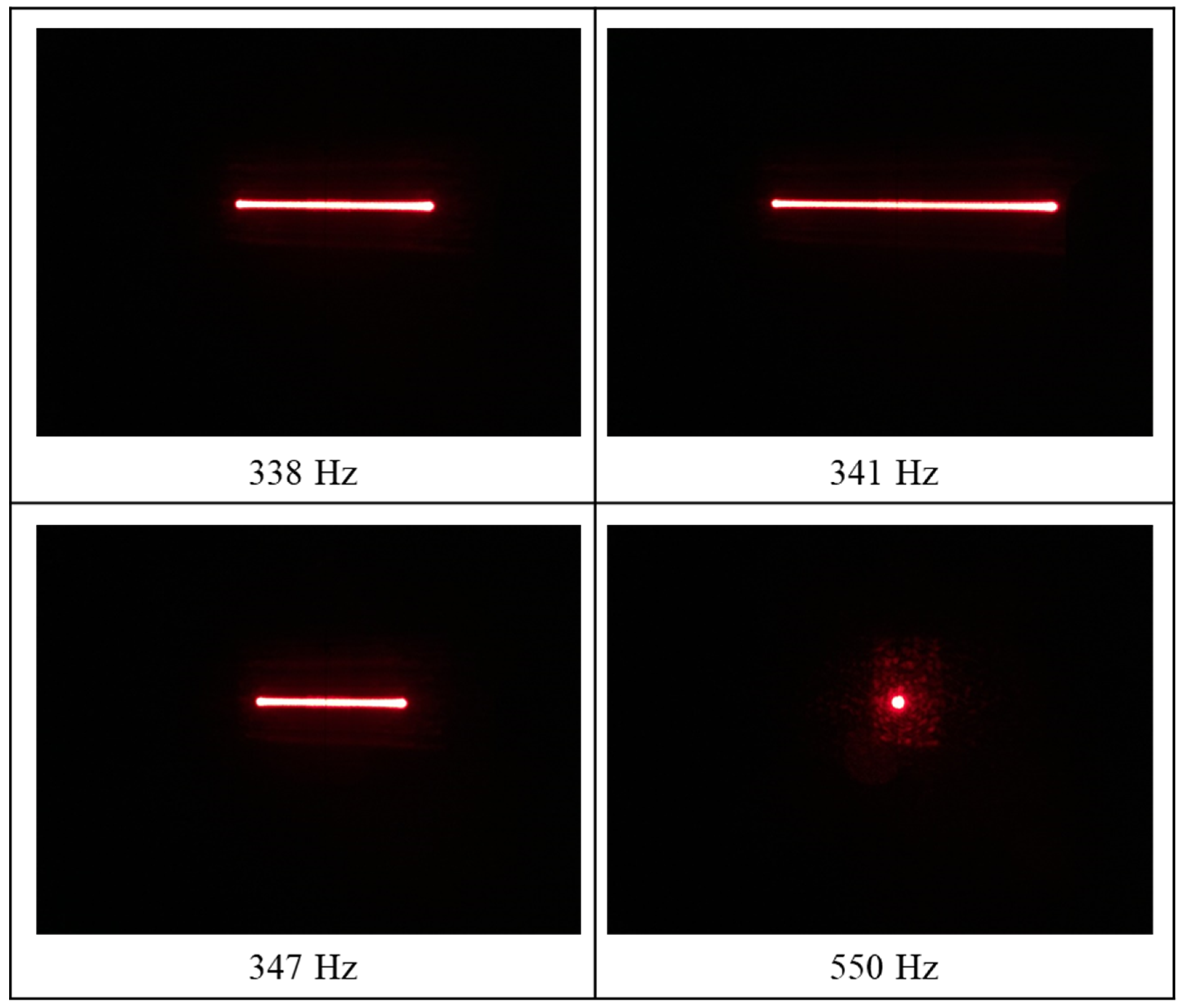
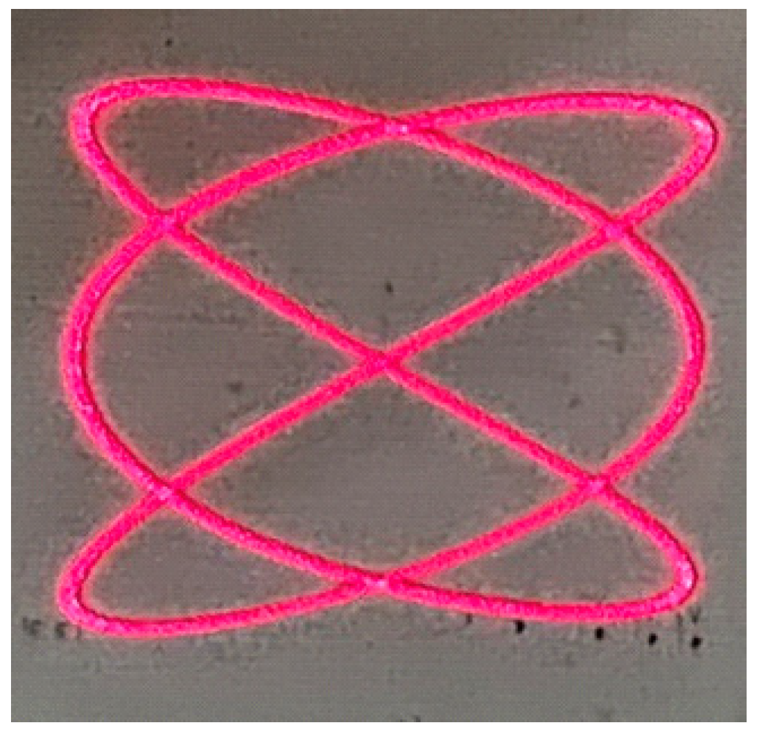
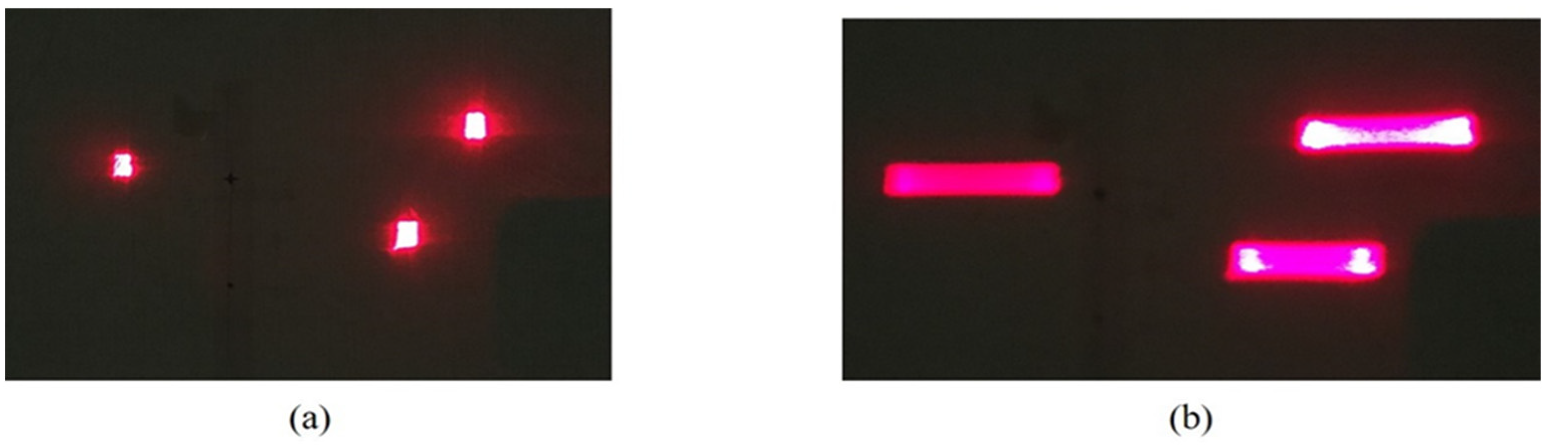
3.2. Experiment Results

Figure 6 shows the static characteristics, optical half angle vs. voltage, of all of the devices. Among all of the devices, Device A has the largest mirror size (20 × 20 mm2) and does not have the soft iron core for extension; it exhibits the largest optical deflection angle. At a 12 V dc voltage, the optical half angle θhalf is as large as 14.8 degrees, which means the full scan range of this scanner is 29.6 degrees under quasi-static operation. This is a considerable angular range for a mirror-type beam scanner.
Figure 7 is the frequency response of Device D. The peak-to-peak voltage is kept a constant when the frequency is swept. Based on the frequency response curve, when the driving frequency is 341 Hz, the full optical scan range θfull reaches the maximum; 341 Hz is then the resonance frequency of the device.
Figure 8 shows the traces of the reflected light spot on the screen of Device D at several selected frequencies, including the resonance frequency 341 Hz. It can be seen that the longest trace does occur at the resonance frequency. No rotation around the orthogonal axis is observed.
Table 3 lists the measured mirror frame thickness, spring size, and torsional resonance frequency of each device, as well as the estimated mirror mass (including the silicon slice, coated aluminum, and permanent magnets), estimated torsion and bending spring constants, and predicted torsional and bending resonance frequencies. When calculating the spring constants and mirror mass and predicting the resonance frequencies, we take the measured dimensions instead of the designed values.
As expected, the resonance frequency is mainly related to the mirror geometry and torsion springs. Whether the electromagnet has an iron core for extension or not should not affect the resonance frequency.
The predicted torsion spring constant kt and resonance frequency ft are calculated using the following equations:
k t = 2 K × G L
f t = 1 2 π k t I
where G is the shear modulus of PLA, L is the length of the spring, I is the rotational moment of inertia of the mirror, and K is the shape factor of the spring’s cross section which can be expressed as
K a b 3 [ 16 3 3.36 b a ( 1 b 4 12 a 4 ) ]
where a is half of the spring width, and b is half of the spring thickness [23].
The predicted bending spring constant kb and resonance frequency fb are calculated with:
k b = 32 E a b 3 L 3
f b = 1 2 π k b m
where E is the Young’s modulus of PLA, and m is the mass of the mirror. The Young’s modulus and mass density of PLA chosen for our calculation are 1.36 GPa and 1240 kg/m3, respectively. We will present a further discussion regarding the calculation in the next section.

4. Discussion

The PLA’s Young’s modulus can vary within a wide range [24]. Apparently, the modulus of our device is on the lower side. We assume 1.36 GPa as the Young’s modulus, and the difference between the prediction and actual performance of the torsion mode is smaller than 10%. With the Young’s modulus and mass density set to 1.36 GPa and 1240 kg/m3, respectively, and with the measured spring dimensions and mirror frame’s thickness, we are able to calculate/estimate/predict the resonance frequencies of the bending modes, torsional and bending spring constants, and mass, which are all included in Table 3 above.
In Devices A, D, and E, the bending mode exhibits a frequency far higher than that of the torsion mode, so coupling should be insignificant. In Devices B and C, the difference between the bending and torsion mode frequencies is not as large, but it is still greater than the measured resonance mode width of the torsion mode; therefore, coupling should also be negligible. Furthermore, the two permanent magnets of each mirror are oriented in opposite directions so the net force on the mirror should be minimized, if not zero, making it hard to excite the bending mode significantly. In summary, coupling should be insignificant, and it is unlikely to excite a substantial bending motion. We did verify this experimentally. In our experiments (referring to Figure 5 which shows the setup to find the resonance), we found that d increased with L as expected at any tested frequency, which would not have been possible if the out-of-plane motion, instead of rotation, had been excited; an out-of-plane motion would have resulted in a lateral shift of the laser beam instead of a deflection angle. Moreover, a significant out-of-plane motion would cause the laser beam to miss the mirror, which was never observed during the experiments.
Regarding the effect of any possible misalignment of the permanent magnets, if we take Device A as an example, misalignments of 0.5 mm of the permanent magnets may result in an estimated 7% change in the static angle. In Devices B–E, such misalignments of the permanent magnets may result in an estimated 14% change in the static angle.
Another concern is the consistency between prints, and we can infer from the measured resonance frequencies. Devices B and C have the same mirror frame design, while Devices D and E share the same mirror frame design. As shown in Table 3, the measured resonant frequencies of Devices B and C are 229 and 227 Hz, respectively, i.e., <0.9% difference; the measured resonant frequencies of Devices D and E are 341 and 348 Hz, respectively, i.e., 2% difference. This demonstrates decent consistency between prints.
In terms of device lifetime, the parameters of the printed material can indeed change with time because of environmental factors, such as humidity and temperature. One of our future plans is to perform a long-term monitoring of the devices to study the effect of those factors. From a different point of view, our low-cost devices can be disposable had they become unusable due to those long-term effects from the environmental factors; the rapid prototyping nature of 3D printing can provide fast delivery of a new device.
Our goal is to propose an extremely low-cost scanner solution. The 3D printer costed about 4000 USD, and our estimated material cost per scanner is merely <10 USD (PLA: <0.4 USD; silicon slice + aluminum coating: <2.5 USD; electromagnet: <6.5 USD; permanent magnets: <0.2 USD); no other charge was incurred.
Closed-loop control has been a popular approach for improving scanner performance [25]. However, since we position our work as an extremely low-cost scanner solution, we intentionally avoid the closed-loop control to keep the cost low. We have tested a scanner with a modified but similar design under open-loop operation using a PSD (position sensing detector); the results show good angular repeatability with an error of only ~1.6% (Figure 9).
A scanner can be dedicated to either quasi-static scanning or dynamic scanning. The static characterization demonstrated in Section 3 has proven the ability of our scanners to perform quasi-static scanning. Dynamic scanning includes raster scanning [14], spiral scanning [26], Lissajous scanning [27], etc. Our scanners exhibit static optical full angles of >4 deg.; Devices A and B can even reach 29 deg. and 16 deg., respectively. Moreover, all of the measured resonance frequencies are greater than 60 Hz. Therefore, our devices can serve as the slow-axis scanner for raster scanning with a 60 Hz frame rate. As for Lissajous scanning, using a pair of our revised scanners with minor modification (mainly to increase the mirror area), we are able to generate a nice Lissajous pattern (Figure 10). The frequencies of the x and y scans are 70 and 58 Hz, respectively.
Lastly, an expanded laser beam is shined on a 1 × 3 scanner array (Device B ×2; Device C ×1). The three scanners are intentionally oriented along slightly different directions so that the reflected beams from the scanners can be separated. Figure 11a shows the reflected spots on a screen when no mirror is driven; in Figure 11b the traces of the reflected spots under a driving frequency of 217 Hz are presented. This type of scanner array can potentially be used for simultaneous multiple-beam steering.

5. Conclusions

In this paper, we have presented the designs and experimental results of 3D-printed 1-DOF optical scanners with large mirror areas (up to 20 × 20 mm2). Five different designs have been studied. Each device consists of an aluminum-coated square silicon substrate serving as the mirror, two miniature permanent magnets, an electromagnet, and a 3D-printed structure including the mirror frame, torsion springs, and base. The scanner with a 20 × 20 mm2 mirror area and a measured resonance frequency 84 Hz reaches a static half optical scan angle of 14.8 deg., i.e., a full optical scan angle of 29.6 deg., at 12 V. These scanners can be an extremely low-cost alternative to the conventional expensive galvanometer scanners. Although we have not achieved the 40 deg. seen in some galvanometer scanners, 29.6 deg. at a low voltage of 12 V and operation without needing an amplifier and closed-loop control are definitely attractive. Specifically, the cost of each scanner is <10 USD, which is an overwhelming margin against many competing devices. A short turnaround time of <1 week to complete fabrication and delivery is also appealing.
We have shown good angular repeatability of the scanner and also presented a Lissajous scanning pattern. A 1 × 3 scanner array has also been assembled, and multiple-beam steering implemented by this array has been demonstrated.

Author Contributions

Conceptualization, J.-c.T.; experiment, C.-K.S., Y.-N.H., G.-Y.L., W.-A.T., Y.-W.C., P.-H.Y.; writing, C.-K.S. and J.-c.T. All authors have read and agreed to the published version of the manuscript.

Funding

This research was supported by the Ministry of Science and Technology of Taiwan under Grant MOST 109-2221-E-002-019 and Grant MOST 110-2221-E-002-076.

Data Availability Statement

Data supporting the results reported in this paper may be obtained from the authors upon reasonable request.

Conflicts of Interest

The authors declare no conflict of interest.

References

  1. Aylward, R.P. Advances and technologies of galvanometer-based optical scanners. In Proceedings of the SPIE’S International Symposium on Optical Science, Engineering, and Instrumentation, Denver, CO, USA, 18–23 July 1999. [Google Scholar]
  2. Duma, V.-F. Laser scanners with oscillatory elements: Design and optimization of 1D and 2D scanning functions. Appl. Math. Model. 2018, 67, 456–476. [Google Scholar] [CrossRef]
  3. Li, Y. Single-mirror beam steering system: Analysis and synthesis of high-order conic-section scan patterns. Appl. Opt. 2008, 47, 386–398. [Google Scholar] [CrossRef] [PubMed]
  4. Novanta Photonics. 62xxK and 83xxK Series, Galvanometers. Available online: https://novantaphotonics.com/product/62xxk-and-83xxk-series-galvanometers/ (accessed on 22 June 2022).
  5. Thorlabs. Galvanometers. Available online: https://www.thorlabs.com/navigation.cfm?guide_id=2269 (accessed on 22 June 2022).
  6. Scanlab. Galvanometer Scanners. Available online: https://www.scanlab.de/en/products/galvanometer-scanners (accessed on 22 June 2022).
  7. Salimi, M.H.; Villiger, M.; Tabatabaei, N. New Model for Understanding the Relationship between Tissue Composition and Photothermal Optical Coherence Tomography Signals. In Proc. SPIE 11655, Label-Free Biomedical Imaging and Sensing (LBIS) 2021; SPIE Proceedings: Bellingham, WA, USA, 2021. [Google Scholar] [CrossRef]
  8. Luo, Y.; Arauz, L.J.; Castillo, J.E.; Barton, J.K.; Kostuk, R.K. Parallel optical coherence tomography system. Appl. Opt. 2007, 46, 8291–8297. [Google Scholar] [CrossRef] [PubMed] [Green Version]
  9. Cui, M.; Lin, J.; Cheng, Z.; Gan, W. Jitter suppression for resonant galvo based high-throughput laser scanning systems. Opt. Express 2020, 28, 26414–26420. [Google Scholar] [CrossRef]
  10. Li, Y.; Cui, T.; Li, Q.; Zhang, B.; Bai, Y.; Wang, C. A study of correction method to the pincushion distortion based on dual galvanometer LiDAR scanning system. Optik 2019, 181, 555–561. [Google Scholar] [CrossRef]
  11. Wang, Q.; Wang, W.; Zhuang, X.; Zhou, C.; Fan, B. Development of an Electrostatic Comb-Driven MEMS Scanning Mirror for Two-Dimensional Raster Scanning. Micromachines 2021, 12, 378. [Google Scholar] [CrossRef] [PubMed]
  12. Strathman, M.; Liu, Y.; Keeler, E.G.; Song, M.; Baran, U.; Xi, J.; Sun, M.T.; Wang, R.; Li, X.; Lin, L.Y. MEMS scanning micromirror for optical coherence tomography. Biomed. Optics Express 2015, 6, 211–224. [Google Scholar] [CrossRef] [PubMed] [Green Version]
  13. Gorecki, C.; Bargiel, S. MEMS Scanning Mirrors for Optical Coherence Tomography. Photonics 2020, 8, 6. [Google Scholar] [CrossRef]
  14. Yalcinkaya, A.D.; Urey, H.; Brown, D.; Montague, T.; Sprague, R. Two-Axis Electromagnetic Microscanner for High Resolution Displays. J. Microelectromech. Syst. 2006, 15, 786–794. [Google Scholar] [CrossRef]
  15. Tanguy, Q.A.A.; Gaiffe, O.; Passilly, N.; Cote, J.-M.; Cabodevila, G.; Bargiel, S.; Lutz, P.; Xie, H.; Gorecki, C. Real-time Lissajous imaging with a low-voltage 2-axis MEMS scanner based on electrothermal actuation. Opt. Express 2020, 28, 8512–8527. [Google Scholar] [CrossRef] [PubMed]
  16. Hashimoto, M.; Taguchi, Y. Design and Fabrication of a Kirigami-Inspired Electrothermal MEMS Scanner with Large Dis-placement. Micromachines 2020, 11, 362. [Google Scholar] [CrossRef] [PubMed] [Green Version]
  17. Senger, F.; Albers, J.; Hofmann, U.; Piechotta, G.; Giese, T.; Heinrich, F.; von Wantoch, T.; Gu-Stoppel, S. A bi-axial vacu-um-packaged piezoelectric MEMS mirror for smart headlights. In MOEMS and Miniaturized Systems XIX; SPIE Proceedings: Bellingham, WA, USA, 2020; Volume 1129305. [Google Scholar]
  18. Kim, J.; Lee, H.; Kim, B.; Jeon, J.; Yoon, J.; Yoon, E. A high fill-factor micro-mirror stacked on a crossbar torsion spring for electrostatically-actuated two-axis operation in large-scale optical switch. In Proceedings of the Sixteenth Annual International Conference on Micro Electro Mechanical Systems, Kyoto, Japan, 23–23 January 2003. [Google Scholar] [CrossRef]
  19. Conant, R.A.; Nee, J.T.; Lau, K.Y.; Muller, R.S. A flat high-frequency scanning micromirror. In Proceedings of the Technical Digest 2000 Solid-State Sensor & Actuator Workshop, Hilton Head Island, SC, USA, 4–8 June 2000; pp. 6–9. [Google Scholar]
  20. Duma, V.-F.; Dimb, A.-L. Exact Scan Patterns of Rotational Risley Prisms Obtained with a Graphical Method: Multi-Parameter Analysis and Design. Appl. Sci. 2021, 11, 8451. [Google Scholar] [CrossRef]
  21. Li, A.; Yi, W.; Zuo, Q.; Sun, W. Performance characterization of scanning beam steered by tilting double prisms. Opt. Express 2016, 24, 23543. [Google Scholar] [CrossRef]
  22. Li, Y. Third-order theory of the Risley-prism-based beam steering system. Appl. Opt. 2011, 50, 679–686. [Google Scholar] [CrossRef] [PubMed]
  23. Urey, H. Torsional MEMS scanner design for high-resolution scanning display systems. In Optical Scanning; SPIE Proceedings: Bellingham, WA, USA, 2002; Volume 4773, pp. 27–38. [Google Scholar] [CrossRef] [Green Version]
  24. Farah, S.; Anderson, D.G.; Langer, R. Physical and mechanical properties of PLA, and their functions in widespread applications—A comprehensive review. Adv. Drug Delivery Rev. 2016, 107, 367–392. [Google Scholar] [CrossRef] [PubMed] [Green Version]
  25. Hayakawa, T.; Watanabe, T.; Senoo, T.; Ishikawa, M. Gain-compensated sinusoidal scanning of a galvanometer mirror in proportional-integral-differential control using the pre-emphasis technique for motion-blur compensation. Appl. Opt. 2016, 55, 5640–5646. [Google Scholar] [CrossRef] [PubMed]
  26. Carrasco-Zevallos, O.M.; Viehland, C.; Keller, B.; McNabb, R.P.; Kuo, A.N.; Izatt, J.A. Constant linear velocity spiral scanning for near video rate 4D OCT ophthalmic and surgical imaging with isotropic transverse sampling. Biomed. Opt. Express 2018, 9, 5052–5070. [Google Scholar] [CrossRef] [PubMed]
  27. Hwang, K.; Seo, Y.-H.; Ahn, J.; Kim, P.; Jeong, K.-H. Frequency selection rule for high definition and high frame rate Lissajous scanning. Sci. Rep. 2017, 7, 14075. [Google Scholar] [CrossRef] [PubMed]
Figure 1. Exploded view drawing of the device.
Photonics 09 00484 g001
Figure 2. Two practical arrangements: (a) Type I without the soft iron core for extension; (b) Type II with the soft iron core for extension.
Photonics 09 00484 g002
Figure 3. The photos of the fabricated devices: (a) Device A (b) Device B (c) Device C (d) Device D (e) Device E.
Photonics 09 00484 g003
Figure 4. dc characterization: (a) experimental setup; (b) the optical half angle (θhalf) can be found using the given L and measured d.
Photonics 09 00484 g004
Figure 5. Dynamic characterization: (a) experimental setup; (b) the full optical scan range [θfull = 2 θhalf = 2tan−1(d/2L)] at a certain voltage amplitude and frequency can be found using the given L and measured d; the frequency response can be obtained by sweeping the frequency of the function generator.
Photonics 09 00484 g005
Figure 6. Static characteristics: optical half angle θhalf vs. dc voltage for different devices.
Photonics 09 00484 g006
Figure 7. The frequency response of Device D.
Photonics 09 00484 g007
Figure 8. Traces of the reflected light spot on the screen of Device D at several selected frequencies, including the resonance frequency 341 Hz.
Photonics 09 00484 g008
Figure 9. PSD output of the scanner angular repeatability test. The output voltage amplitude is ~5 V with variation of <0.08 V, i.e., ~1.6%.
Photonics 09 00484 g009
Figure 10. Lissajous scanning with the frequencies of the x and y scans being 70 and 58 Hz, respectively.
Photonics 09 00484 g010
Figure 11. (a) Reflected spots on a screen from a 1 × 3 scanner array when no mirror is driven; (b) Traces of the reflected spots under a driving frequency of 217 Hz.
Photonics 09 00484 g011
Table 1. Schematic 3D drawings and designed dimensions of the five different designed devices.
Oblique Top ViewSide ViewBottom View
(Beneath the Mirror)
A (Type I) Photonics 09 00484 i001 Photonics 09 00484 i002 Photonics 09 00484 i003
B (Type I) Photonics 09 00484 i004 Photonics 09 00484 i005 Photonics 09 00484 i006
C (Type II) Photonics 09 00484 i007 Photonics 09 00484 i008 Photonics 09 00484 i009
D (Type I) Photonics 09 00484 i010 Photonics 09 00484 i011 Photonics 09 00484 i012
E (Type II) Photonics 09 00484 i013 Photonics 09 00484 i014 Photonics 09 00484 i015
Table 2. Specifications of the designed devices.
A (Type I)B (Type I)C (Type II)D (Type I)E (Type II)
Mirror frame size (mm3)20 × 20 × 310 × 10 × 110 × 10 × 110 × 10 × 110 × 10 × 1
Torsion spring size (mm3)10 × 1.5 × 110 × 1 × 0.510 × 1 × 0.55 × 1 × 0.55 × 1 × 0.5
Table 3. Estimated and measured parameters of each device.
DevicesMeasured Mirror Frame Thickness (mm)Measured Spring Size (mm3, Length × Width × Thickness)Est. Mirror Mass (g)Est. Torsion Spring Const. (N m/rad)Est. Bending Spring Const. (N/m)Predicted Torsional Resonance Freq. (Hz)Predicted Bending Resonance Freq. (Hz)Measured
Torsional
Resonance Freq. (Hz)
Device A2.579.82 × 1.6 × 0.992.583.24 × 10−2446091.25209.1984
Device B1.139.97 × 1.01 × 0.650.2795.56 × 10−3761.2243.94263.02229
Device C1.129.83 × 1.1 × 0.620.2785.76 × 10−3750.6248.66261.77227
Device D1.164.9 × 1.02 × 0.590.2719.1 × 10−34844316.42673.05341
Device E1.154.87 × 1.02 × 0.620.28110.34 × 10−35724331718.07348
Publisher’s Note: MDPI stays neutral with regard to jurisdictional claims in published maps and institutional affiliations.

