Advances in Mid-Infrared Single-Photon Detection

 , ,
, ,
Abstract
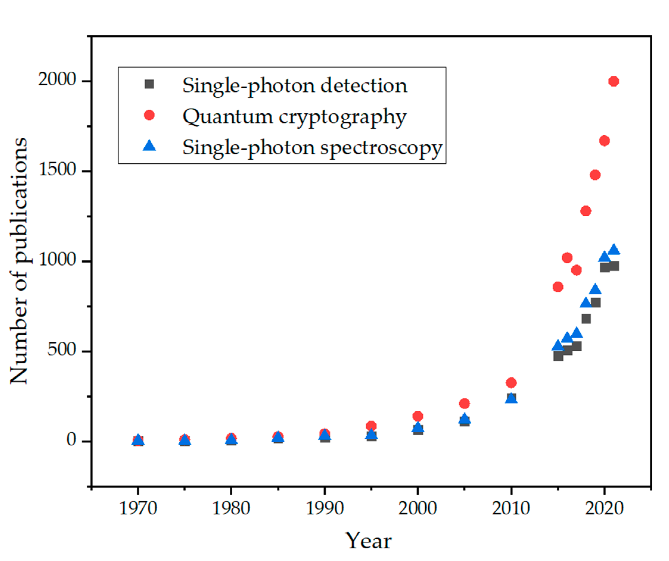
:1. Introduction
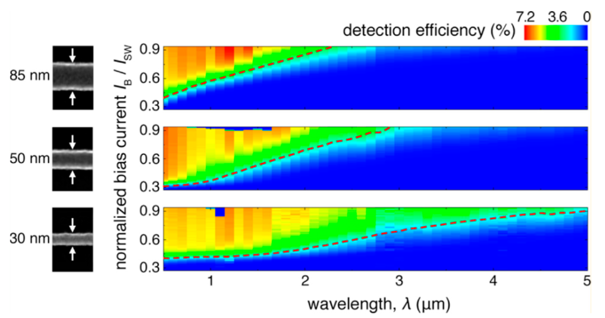
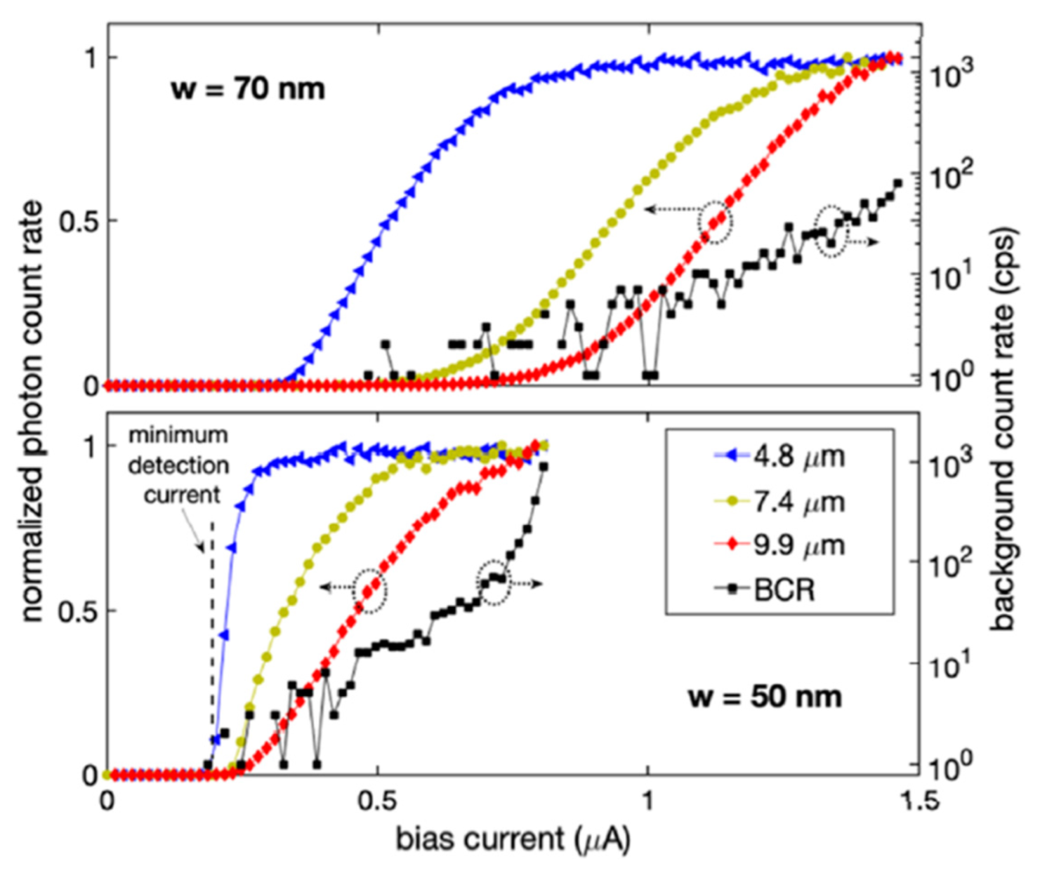
2. Superconducting Nanowire Single-Photon Detectors
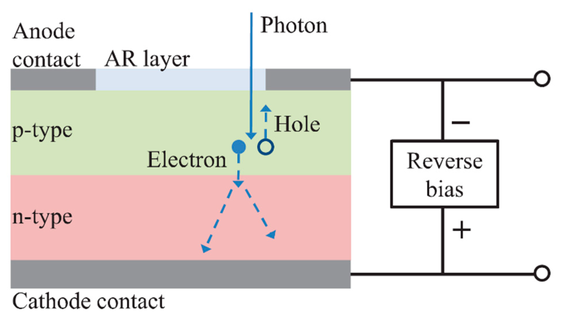
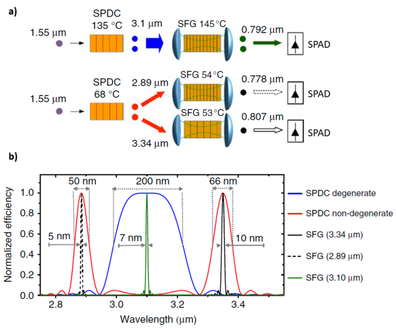
3. Single-Photon Avalanche Diodes
4. Photovoltaic Detectors
5. Conclusions
Author Contributions
Funding
Institutional Review Board Statement
Informed Consent Statement
Data Availability Statement
Conflicts of Interest
References
- Spitz, O.; Didier, P.; Durupt, L.; Diaz-Thomas, D.A.; Baranov, A.N.; Cerutti, L.; Grillot, F. Free-Space Communication With Directly Modulated Mid-Infrared Quantum Cascade Devices. IEEE J. Sel. Top. Quantum Electron. 2022, 28, 1200109. [Google Scholar]
- Shields, T.; Prabhakar, S.; Dada, A.; Ebrahim, M.; Taylor, G.G.; Morozov, D.; Erotokritou, K.; Miki, S.; Yabuno, M.; Terai, H.; et al. Mid-infrared Quantum Interference and Polarization Entanglement. In Proceedings of the OSA High-Brightness Sources and Light-Driven Interactions Congress 2020 (EUVXRAY, HILAS, MICS), Washington, DC, USA, 16–20 November 2020. [Google Scholar]
- Lanning, R.N.; Harris, M.A.; Oesch, D.W.; Oliker, M.D.; Gruneisen, M.T. Quantum Communication Over Atmospheric Channels: A Framework for Optimizing Wavelength and Filtering. Phys. Rev. Appl. 2021, 16, 044027. Available online: http://arxiv.org/abs/2104.10276 (accessed on 15 March 2022).
- Widarsson, M.; Henriksson, M.; Mutter, P.; Canalias, C.; Pasiskevicius, V.; Laurell, F. High resolution and sensitivity up-conversion mid-infrared photon-counting LIDAR. Appl. Opt. 2020, 59, 2365. [Google Scholar]
- Wollman, E.E.; Verma, V.B.; Walter, A.B.; Chiles, J.; Korzh, B.; Allmaras, J.P.; Zhai, Y.; Lita, A.E.; McCaughan, A.N.; Schmidt, E.; et al. Recent advances in superconducting nanowire single-photon detector technology for exoplanet transit spectroscopy in the mid-infrared. J. Astron. Telesc. Instrum. Syst. 2021, 7, 011004. [Google Scholar]
- Chen, L.; Schwarzer, D.; Verma, V.B.; Stevens, M.J.; Marsili, F.; Mirin, R.P.; Nam, S.W.; Wodtke, A.M. Mid-infrared Laser-Induced Fluorescence with Nanosecond Time Resolution Using a Superconducting Nanowire Single-Photon Detector: New Technology for Molecular Science. Acc. Chem. Res. 2017, 50, 1400–1409. [Google Scholar]
- Verma, V.B.; Lita, A.E.; Korzh, B.A.; Wollman, E.; Shaw, M.; Mirin, R.P.; Nam, S.-W. Towards single-photon spectroscopy in the mid-infrared using superconducting nanowire single-photon detectors. In Advanced Photon Counting Techniques XIII, Proceedings of the SPIE Defense + Commercial Sensing, Baltimore, MD, USA, 14–18 April 2019; SPIE: Bellingham, WA, USA, 2019. [Google Scholar]
- Cheng, R.; Zou, C.-L.; Guo, X.; Wang, S.; Han, X.; Tang, H.X. Broadband on-chip single-photon spectrometer. Nat. Commun. 2019, 10, 4104. [Google Scholar]
- von Helversen, M.; Böhm, J.; Schmidt, M.; Gschrey, M.; Schulze, J.-H.; Strittmatter, A.; Rodt, S.; Beyer, J.; Heindel, T.; Reitzenstein, S. Quantum metrology of solid-state single-photon sources using photon-number-resolving detectors. New J. Phys. 2019, 21, 035007. [Google Scholar]
- Chunnilall, C.J.; Degiovanni, I.P.; Kück, S.; Müller, I.; Sinclair, A.G. Metrology of single-photon sources and detectors: A review. Opt. Eng. 2014, 53, 081910. [Google Scholar]
- Temporão, G.; Tanzilli, J.-S.; Zbinden, H.; Gisin, N.; Aellen, T.; Giovannini, M.E.; Faist, J. Mid-infrared single-photon counting. Opt. Lett. 2006, 31, 1094–1096. [Google Scholar]
- Spitz, O.; Herdt, A.; Didier, P.; Elsäßer, W.; Grillot, F. Mid-infrared free-space cryptosystem. Nonlinear Theory Its Appl. IEICE 2022, 13, 44–52. [Google Scholar]
- Grillot, F.; Spitz, O. Chaos-based mid-infrared communications. In Physics and Simulation of Optoelectronic Devices XXX, Proceedings of the SPIE OPTO, San Francisco, CA, USA, 22 January–28 February 2022; SPIE: Bellingham, WA, USA, 2022; Volume 11995, p. 11995. [Google Scholar]
- Gilaberte Basset, M.; Setzpfandt, F.; Steinlechner, F.; Beckert, E.; Pertsch, T.; Gräfe, M. Perspectives for applications of quantum imaging. Laser Photonics Rev. 2019, 13, 1900097. [Google Scholar]
- Available online. Available online: https://scholar.google.com/ (accessed on 15 March 2022).
- Scarani, V.; Bechmann-Pasquinucci, H.; Cerf, N.J.; Dušek, M.; Lütkenhaus, N.; Peev, M. The security of practical quantum key distribution. Rev. Mod. Phys. 2009, 81, 1301–1350. [Google Scholar]
- Pirandola, S.; Andersen, U.L.; Banchi, L.; Berta, M.; Bunandar, D.; Colbeck, R.; Englund, D.; Gehring, T.; Lupo, C.; Ottaviani, C.; et al. Advances in quantum cryptography. Adv. Opt. Photonics 2020, 12, 1012. [Google Scholar]
- Temporao, G.; Zibinden, H.; Tanzilli, S.; Gisin, N.; Aellen, T.; Giovannini, M.; Faist, J.; von der Weid, J. Feasibility study of free-Space quantum key distribution in the mid-infrared. Quantum Inf. Comput. 2008, 8, 1–11. [Google Scholar]
- E490-00a; Standard Solar Constant and Zero Air Mass Solar Spectral Irradiance Tables. ASTM International: West Conshohocken, PA, USA, 2019.
- Prabhakar, S.; Shields, T.; Dada, A.C.; Ebrahim, M.; Taylor, G.G.; Morozov, D.; Erotokritou, K.; Miki, S.; Yabuno, M.; Terai, H.; et al. Two-photon quantum interference and entanglement at 2.1 μm. Sci. Adv. 2020, 6, eaay5195. Available online: https://www.science.org (accessed on 22 March 2022).
- Ellis, A.D.; Mac Suibhne, N.; Saad, D.; Payne, D.N. Communication networks beyond the capacity crunch. Philos. Trans. R. Soc. A Math. Phys. Eng. Sci. 2016, 374, 20150191. [Google Scholar]
- Dada, A.C.; Kaniewski, J.; Gawith, C.; Lavery, M.; Hadfield, R.H.; Faccio, D.; Clerici, M. Near-Maximal Two-Photon Entanglement for Optical Quantum Communication at 2.1 μm. Phys. Rev. Appl. 2021, 16, L051005. [Google Scholar]
- Roberts, P.J.; Couny, F.; Sabert, H.; Mangan, B.J.; Williams, D.P.; Farr, L.; Mason, M.W.; Tomlinson, A.; Birks, T.; Knight, J.; et al. Ultimate low loss of hollow-core photonic crystal fibres. Opt. Express 2005, 13, 236. [Google Scholar]
- Widarsson, M.; Henriksson, M.; Barrett, L.; Pasiskevicius, V.; Laurell, F. Room temperature photon-counting lidar at 3 µm. Appl. Opt. 2022, 61, 884. [Google Scholar]
- Haas, J.; Mizaikoff, B. Advances in Mid-Infrared Spectroscopy for Chemical Analysis. Annu. Rev. Anal. Chem. 2016, 9, 45–68. [Google Scholar]
- Bukowski, R.W. Smoke measurements in large- and small-scale fire testing—Part I. Fire Technol. 1979, 15, 173–179. [Google Scholar]
- Chen, Y.; Xue, L.; Zhu, Q.; Feng, Y.; Wu, M. Recent advances in second near-infrared region (NIR-II) fluorophores and biomedical applications. Front. Chem. 2021, 9, 750404. [Google Scholar]
- Yu, J.; Zhang, R.; Gao, Y.; Sheng, Z.; Gu, M.; Sun, Q.; Liao, J.; Wu, T.; Lin, Z.; Wu, P.; et al. Intravital confocal fluorescence lifetime imaging microscopy in the second near-infrared window. Opt. Lett. 2020, 45, 3305–3308. [Google Scholar]
- Ravaro, M.; Locatelli, M.; Pugliese, E.; Di Leo, I.; de Cumis, M.S.; D’Amato, F.; Poggi, P.; Consolino, L.; Meucci, R.; Ferraro, P.; et al. Mid-infrared digital holography and holographic interferometry with a tunable quantum cascade laser. Opt. Lett. 2014, 39, 4843. [Google Scholar]
- Locatelli, M.; Pugliese, E.; Paturzo, M.; Bianco, V.; Finizio, A.; Pelagotti, A.; Poggi, P.; Miccio, L.; Meucci, R.; Ferraro, P. Imaging live humans through smoke and flames using far-infrared digital holography. Opt. Express 2013, 21, 5379. [Google Scholar]
- Sanna, M.; Rizzotti, D.; Signorini, S.; Pavesi, L. An integrated entangled photons source for mid-infrared ghost spectroscopy. In Quantum Sensing and Nano Electronics and Photonics XVIII, Proceedings of the SPIE OPTO, San Francisco, CA, USA, 22 January–28 February 2022; SPIE: Bellingham, WA, USA, 2022. [Google Scholar]
- Eisaman, M.D.; Fan, J.; Migdall, A.; Polyakov, S.V. Invited Review Article: Single-photon sources and detectors. Rev. Sci. Instrum. 2011, 82, 071101. [Google Scholar]
- Hadfield, R.H. Single-photon detectors for optical quantum information applications. Nat. Photonics 2009, 3, 696–705. [Google Scholar]
- Buller, G.S.; Collins, R.J. Single-photon generation and detection. Meas. Sci. Technol. 2010, 21, 012002. [Google Scholar]
- Chen, Q.; Ge, R.; Zhang, L.; Li, F.; Zhang, B.; Jin, F.; Han, H.; Dai, Y.; He, G.; Fei, Y.; et al. Mid-infrared single photon detector with superconductor Mo80Si20 nanowire. arXiv 2020, arXiv:2011.06699, preprint. [Google Scholar]
- Gol’Tsman, G.N.; Okunev, O.; Chulkova, G.; Lipatov, A.; Semenov, A.; Smirnov, K.; Voronov, B.; Dzardanov, A.; Williams, C.; Sobolewski, R. Picosecond superconducting single-photon optical detector. Appl. Phys. Lett. 2001, 79, 705–707. [Google Scholar]
- Engel, A.; Renema, J.J.; Il’In, K.; Semenov, A. Detection mechanism of superconducting nanowire single-photon detectors. Supercond. Sci. Technol. 2015, 28, 114003. [Google Scholar]
- Korneeva, Y.P.; Mikhailov, M.Y.; Pershin, Y.P.; Manova, N.N.; Divochiy, A.V.; Vakhtomin, Y.B.; Korneev, A.A.; Smirnov, K.V.; Sivakov, A.G.; Devizenko, A.Y.; et al. Superconducting single-photon detector made of MoSi film. Supercond. Sci. Technol. 2014, 27, 095012. [Google Scholar]
- Zadeh, I.E.; Chang, J.; Los, J.W.N.; Gyger, S.; Elshaari, A.W.; Steinhauer, S.; Dorenbos, S.N.; Zwiller, V. Superconducting nanowire single-photon detectors: A perspective on evolution, state-of-the-art, future developments, and applications. Appl. Phys. Lett. 2021, 118, 190502. [Google Scholar]
- Holzman, I.; Ivry, Y. Superconducting Nanowires for Single-Photon Detection: Progress, Challenges, and Opportunities. Adv. Quantum Technol. 2019, 2, 1800058. [Google Scholar]
- Wang, Y.; Li, H.; You, L.X.; Lv, C.L.; Wang, H.Q.; Zhang, X.Y.; Zhang, W.J.; Zhou, H.; Zhang, L.; Yang, X.Y.; et al. Wavelength dependence of intrinsic detection efficiency of NbN superconducting nanowire single-photon detector. Chin. Phys. B 2019, 28, 078. [Google Scholar]
- Marsili, F.; Verma, V.B.; Stern, J.A.; Harrington, S.; Lita, A.E.; Gerrits, T.; Vayshenker, I.; Baek, B.; Shaw, M.D.; Mirin, R.; et al. Detecting Single Infrared Photons with 93% System Efficiency. Nat. Photonics 2012, 7, 210–214. [Google Scholar]
- Shibata, H.; Shimizu, K.; Takesue, H.; Tokura, Y. Ultimate low system dark-count rate for superconducting nanowire single-photon detector. Opt. Lett. 2015, 40, 3428. [Google Scholar]
- Korzh, B.; Zhao, Q.-Y.; Allmaras, J.; Frasca, S.; Autry, T.M.; Bersin, E.A.; Beyer, A.D.; Briggs, R.M.; Bumble, B.; Colangelo, M.; et al. Demonstrating sub-3 ps temporal resolution in a superconducting nanowire single-photon detector. Nat. Photon 2020, 14, 250–255. Available online: http://arxiv.org/abs/1804.06839 (accessed on 5 March 2022).
- Vetter, A.; Ferrari, S.; Rath, P.; Alaee, R.; Kahl, O.; Kovalyuk, V.; Diewald, S.; Goltsman, G.N.; Korneev, A.; Rockstuhl, C.; et al. Cavity-Enhanced and Ultrafast Superconducting Single-Photon Detectors. Nano Lett. 2016, 16, 7085–7092. [Google Scholar]
- Yamashita, T.; Miki, S.; Terai, H. Recent Progress and Application of Superconducting Nanowire Single-Photon Detectors. IEICE Trans. Electron. 2017, E100.C, 274–282. [Google Scholar]
- Korneev, A.; Korneeva, Y.; Florya, I.; Voronov, B.; Goltsman, G. NbN Nanowire Superconducting Single-Photon Detector for Mid-Infrared. Phys. Procedia 2012, 36, 72–76. [Google Scholar]
- Verma, V.B.; Korzh, B.; Walter, A.B.; Lita, A.E.; Briggs, R.M.; Colangelo, M.; Zhai, Y.; Wollman, E.E.; Beyer, A.D.; Allmaras, J.P.; et al. Single-photon detection in the mid-infrared up to 10 μm wavelength using tungsten silicide superconducting nanowire detectors. APL Photonics 2021, 6, 056101. [Google Scholar]
- Marsili, F.; Bellei, F.; Najafi, F.; Dane, A.E.; Dauler, E.A.; Molnar, R.J.; Berggren, K.K. Efficient Single Photon Detection from 500 nm to 5 μm Wavelength. Nano Lett. 2012, 12, 4799–4804. [Google Scholar]
- Marsili, F.; Najafi, F.; Dauler, E.; Bellei, F.; Hu, X.; Csete, M.; Molnar, R.J.; Berggren, K.K. Single-photon detectors based on ultra-narrow superconducting nanowires. Nano Lett. 2011, 11, 2048–2053. [Google Scholar]
- Gisin, N.; Thew, R. Quantum Communication. Nat. Photonics 2007, 1, 165–171. [Google Scholar]
- Zolotov, P.I.; Divochiy, A.V.; Vakhtomin, Y.B.; Morozov, P.V.; Seleznev, V.A.; Smirnov, K.V. Development of high-effective superconducting single-photon detectors aimed for mid-IR spectrum range. J. Phys. Conf. Ser. 2017, 917, 062037. [Google Scholar]
- Chang, J.; Los, J.W.; Gourgues, R.; Steinhauer, S.; Dorenbos, S.N.; Pereira, S.F.; Urbach, H.P.; Zwiller, V.; Zadeh, I.E. Efficient mid-infrared single-photon detection using superconducting NbTiN nanowires with high time resolution in a Gifford-McMahon cryocooler. Photonics Res. 2022, 10, 1063. [Google Scholar]
- Baek, B.; Lita, A.E.; Verma, V.; Nam, S.W. Superconducting a-WxSi1−x nanowire single-photon detector with saturated internal quantum efficiency from visible to 1850 nm. Appl. Phys. Lett. 2011, 98, 251105. [Google Scholar]
- Taylor, G.G.; Morozov, D.; Gemmell, N.R.; Erotokritou, K.; Miki, S.; Terai, H.; Hadfield, R.H. Photon counting LIDAR at 2.3 µm wavelength with superconducting nanowires. Opt. Express 2019, 27, 38147–38158. [Google Scholar]
- Guan, Y.; Li, H.; Xue, L.; Yin, R.; Zhang, L.; Wang, H.; Zhu, G.; Kang, L.; Chen, J.; Wu, P. Lidar with superconducting nanowire single-photon detectors: Recent advances and developments. Opt. Lasers Eng. 2022, 156, 107102. [Google Scholar]
- Rockwell, A.K.; Ren, M.; Woodson, M.; Jones, A.; March, S.D.; Tan, Y.; Yuan, Y.; Sun, Y.; Hool, R.; Maddox, S.J.; et al. Toward deterministic construction of low noise avalanche photodetector materials. Appl. Phys. Lett. 2018, 113, 102106. [Google Scholar]
- Lee, S.; Kodati, S.H.; Guo, B.; Jones, A.H.; Schwartz, M.; Winslow, M.; Grein, C.H.; Ronningen, T.J.; Campbell, J.C.; Krishna, S. Low noise Al0.85Ga0.15As0.56Sb0.44 avalanche photodiodes on InP substrates. Appl. Phys. Lett. 2021, 118, 081106. [Google Scholar]
- Yi, X.; Xie, S.; Liang, B.; Lim, L.W.; Cheong, J.S.; Debnath, M.C.; Huffaker, D.L.; Tan, C.H.; David, J.P.R. Extremely low excess noise and high sensitivity AlAs0.56Sb0.44 avalanche photodiodes. Nat. Photonics 2019, 13, 683–686. [Google Scholar]
- Kang, Y.; Zadka, M.; Litski, S.; Sarid, G.; Morse, M.; Paniccia, M.J.; Kuo, Y.H.; Bowers, J.; Beling, A.; Liu, H.D.; et al. Epitaxially-grown Ge/Si avalanche photodiodes for 1.3 μm light detection. Opt. Express 2008, 16, 9365. [Google Scholar]
- Zhang, J.; Itzler, M.A.; Zbinden, H.; Pan, J.W. Advances in InGaAs/InP single-photon detector systems for quantum communication. Light Sci. Appl. 2015, 4, 286. [Google Scholar]
- Ribordy, G.; Gautier, J.-D.; Zbinden, H.; Gisin, N. Performance of InGaAs/InP avalanche photodiodes as gated-mode photon counters. Appl. Opt. 1998, 37, 2272–2277. [Google Scholar]
- Namekata, N.; Sasamori, S.; Inoue, S. 800 MHz single-photon detection at 1550-nm using an InGaAs/InP avalanche photodiode operated with a sine wave gating. Opt. Express 2006, 14, 10043–10049. [Google Scholar]
- Jiang, W.-H.; Gao, X.-J.; Fang, Y.-Q.; Liu, J.-H.; Zhou, Y.; Jiang, L.-Q.; Chen, W.; Jin, G.; Zhang, J.; Pan, J.-W. Miniaturized high-frequency sine wave gating InGaAs/InP single-photon detector. Rev. Sci. Instrum. 2018, 89, 123104. [Google Scholar]
- Yuan, Z.; Kardynal, B.E.; Sharpe, A.W.; Shields, A.J. High speed single photon detection in the near infrared. Appl. Phys. Lett. 2007, 91, 041114. [Google Scholar]
- Lu, Z.; Sun, W.; Zheng, X.; Campbell, J.; Jiang, X.; Itzler, M.A. Balanced InGaAs/InP avalanche photodiodes for single photon detection. In Biosensing and Nanomedicine V, Proceedings of the SPIE NanoScience + Engineering, San Diego, CA, USA, 12–16 August 2012; SPIE: Bellingham, WA, USA, 2012; Volume 8460. [Google Scholar]
- Kopytko, M.; Sobieski, J.; Gawron, W.; Martyniuk, P. Study of HgCdTe (100) and HgCdTe (111)B Heterostructures Grown by MOCVD and Their Potential Application to APDs Operating in the IR Range up to 8 µm. Sensors 2022, 22, 924. [Google Scholar]
- Dehzangi, A.; Li, J.; Gautam, L.; Razeghi, M. Avalanche Photodetector Based on InAs/InSb Superlattice. Quantum Rep. 2020, 2, 591–599. [Google Scholar]
- Li, J.; Dehzangi, A.; Brown, G.; Razeghi, M. Mid-wavelength infrared avalanche photodetector with AlAsSb/GaSb superlattice. Sci. Rep. 2021, 11, 7104. [Google Scholar]
- Huang, J.; Zhao, C.; Nie, B.; Xie, S.; Kwan, D.C.M.; Meng, X.; Zhang, Y.; Huffaker, D.L.; Ma, W. High-performance mid-wavelength InAs avalanche photodiode using AlAs013Sb087 as the multiplication layer. Photonics Res. 2020, 8, 755. [Google Scholar]
- Mancinelli, M.; Trenti, A.; Piccione, S.; Fontana, G.; Dam, J.S.; Tidemand-Lichtenberg, P.; Pedersen, C.; Pavesi, L. Mid-infrared coincidence measurements on twin photons at room temperature. Nat. Commun. 2017, 8, 15184. [Google Scholar]
- Dam, J.S.; Pedersen, C.; Tidemand-Lichtenberg, P. Room temperature mid-IR single photon spectral imaging. Nat. Photonics 2012, 6, 788–793. [Google Scholar]
- Huang, K.; Wang, Y.; Fang, J.; Kang, W.; Sun, Y.; Liang, Y.; Hao, Q.; Yan, M.; Zeng, H. Mid-infrared photon counting and resolving via efficient frequency upconversion. Photonics Res. 2021, 9, 259. [Google Scholar]
- Rogalski, A. HgCdTe infrared detector material: History, status and outlook. Rep. Prog. Phys. 2005, 68, 2267–2336. [Google Scholar]
- Rogalski, A.; Antoszewski, J.; Faraone, L. Third-generation infrared photodetector arrays. J. Appl. Phys. 2009, 105, 091101. [Google Scholar]
- Yadav, P.V.K.; Ajitha, B.; Kumar Reddy, Y.A.; Sreedhar, A. Recent advances in development of nanostructured photodetectors from ultraviolet to infrared region: A review. Chemosphere 2021, 279, 130473. [Google Scholar]
- Gabbrielli, T.; Cappelli, F.; Bruno, N.; Corrias, N.; Borri, S.; De Natale, P.; Zavatta, A. Mid-infrared homodyne balanced detector for quantum light characterization. Opt. Express 2021, 29, 14536. [Google Scholar]
- Riek, C.; Seletskiy, D.V.; Moskalenko, A.S.; Schmidt, J.F.; Krauspe, P.; Eckart, S.; Eggert, S.; Burkard, G.; Leitenstorfer, A. Direct sampling of electric-field vacuum fluctuations. Science 2015, 350, 420–423. [Google Scholar]
- Pupeza, I.; Huber, M.; Trubetskov, M.; Schweinberger, W.; Hussain, S.A.; Hofer, C.; Fritsch, K.; Poetzlberger, M.; Vamos, L.; Fill, E.; et al. Field-resolved infrared spectroscopy of biological systems. Nature 2020, 577, 52–59. [Google Scholar]
- Kowligy, A.S.; Timmers, H.; Lind, A.J.; Elu, U.; Cruz, F.C.; Schunemann, P.G.; Biegert, J.; Diddams, S.A. Infrared electric field sampled frequency comb spectroscopy. Sci. Adv. 2019, 5, 8794. [Google Scholar]


| Detector Type | Material | Wavelength (µm) | ηQE | ηDE | DCR | T (K) | Ref |
|---|---|---|---|---|---|---|---|
| SNSPD | NbN | 0.5–5 | 0.5–5.5% | 100 cps | 1.5 | [49] | |
| WSi | 4.8; 7.4; 9.9 | 100% | 100 cps | 0.85 | [48] | ||
| Mo80Si20 | 1.55–5.07 | 100% | <100 cps | 0.08 | [35] | ||
| NbTiN | 2–4 | 100% up to 3 µm | 70% @ 2 µm | 2.5 | [53] | ||
| SPAD * | Si-based | 3.1 | 65% | 0.35% | 1 kcps | 300 | [71] |
| Si-based | 3 | 37% | [73] | ||||
| PV | HgCdTe | 4.47 4.72 | 41% 33% | 300 | [77] |
Publisher’s Note: MDPI stays neutral with regard to jurisdictional claims in published maps and institutional affiliations. |
© 2022 by the authors. Licensee MDPI, Basel, Switzerland. This article is an open access article distributed under the terms and conditions of the Creative Commons Attribution (CC BY) license (https://creativecommons.org/licenses/by/4.0/).
Share and Cite
Dello Russo, S.; Elefante, A.; Dequal, D.; Pallotti, D.K.; Santamaria Amato, L.; Sgobba, F.; Siciliani de Cumis, M. Advances in Mid-Infrared Single-Photon Detection. Photonics 2022, 9, 470. https://doi.org/10.3390/photonics9070470
Dello Russo S, Elefante A, Dequal D, Pallotti DK, Santamaria Amato L, Sgobba F, Siciliani de Cumis M. Advances in Mid-Infrared Single-Photon Detection. Photonics. 2022; 9(7):470. https://doi.org/10.3390/photonics9070470
Chicago/Turabian StyleDello Russo, Stefano, Arianna Elefante, Daniele Dequal, Deborah Katia Pallotti, Luigi Santamaria Amato, Fabrizio Sgobba, and Mario Siciliani de Cumis. 2022. "Advances in Mid-Infrared Single-Photon Detection" Photonics 9, no. 7: 470. https://doi.org/10.3390/photonics9070470