Article

Design and Simulation of Linear All-Optical Comparator Based on Square-Lattice Photonic Crystals

1
Department of Electrical Engineering, Kermanshah Branch, Islamic Azad University, Kermanshah 67189-97551, Iran
2
Nano-Photonics and Optoelectronics Research Laboratory (NORLab), Shahid Rajaee Teacher Training University, Tehran 16788-15811, Iran
*
Author to whom correspondence should be addressed.
Photonics 2022, 9(7), 459; https://doi.org/10.3390/photonics9070459
Submission received: 24 May 2022 / Revised: 26 June 2022 / Accepted: 27 June 2022 / Published: 29 June 2022
(This article belongs to the Section Optoelectronics and Optical Materials)

Abstract

:
An optical comparator is an important logic circuit used in digital designs. Photonic crystals are among the platforms for implementing different kinds of gates and logic circuits, and they are structures with alternating refractive indices. In this paper, an optical comparator is designed and simulated based on a square lattice photonic crystal. In the design of this comparator, a small-sized structure is used. The simulation results show that in the proposed comparator, there is a high difference between logical values “0” and “1”, which are defined based on the optical power level. Due to the small size of this comparator and the adequate difference between logical values “0” and “1”, this structure suits photonic integrated circuits with high accuracy. The proposed structure footprint is 149.04 µm2, and the calculated rise time for this circuit is less than 0.4 ps.

1. Introduction

Electrons are considered the charge carriers in electronic circuits. In these circuits, a transistor serves as the base part. In other words, all circuits are designed using transistors. Since the movement of electrons in transistors is determined by the size of this part, the speed of the transistor circuits is limited by the size of the transistors [1,2,3,4]. If electronic parts are replaced with optical parts, the photons play the role of charge carriers. Given the high speed of photons, if optical parts are used, their speed will increase drastically. Therefore, it is better to use optical circuits to design high-speed integrated circuits [5,6,7,8,9].
Photonic crystals are among the platforms that suit the design of optical circuits. One of the reasons for paying more attention to this structure is that it is possible to design different types of circuits using photonic crystals. Many logic gates have been designed with photonic crystals [10,11,12,13,14,15,16,17]. Moreover, many logic circuits such as adders, subtractors, decoders, encoders, and de-multiplexers have been designed [18,19,20,21,22,23,24,25,26]. The two-bit comparator is among the logic circuits. This circuit compares two bits. Very few studies have been conducted on the design of optical comparators with photonic crystals [27,28,29,30,31,32,33,34].
Recently, several papers have been penned on the design of comparators. In 2017, Rathi et al. designed a small-sized structure for an optical comparator based on square-lattice photonic crystals. This paper shows that the structure can act as a comparator using optical power distribution, and the output values are not determined quantitatively [27]. In 2018, Fakouri-Farid et al. used a square-lattice photonic crystal structure to design a comparator. The difference between the high and low logical values was acceptable in this comparator, but the size of the structure was extremely large. Moreover, due to the use of a ring resonator in the structure, the delay time of the circuit is increased [28].
Another comparator was designed by Serajmohammadi et al. in 2019. In this paper, the difference between the high and low logical values was satisfactory, but the circuit size was large, and a ring resonator was used [29]. Another structure was designed by Surendar et al. in 2019. In this structure, three ring resonators with non-linear rods having several point defects were used. The design of this structure seems difficult due to its large dimensions as well as the use of non-linear rods of different sizes [30].
A comparator was also designed in 2019 by Jalali et al. This structure also consists of four ring resonators, which increase the circuit size and the circuit delay time [31]. In 2020, Seraj et al. designed a comparator based on photonic crystals. Despite the small size of this structure, the difference between the high and low logical values is not appropriate [32].
In 2019, Zhu et al. designed a one-bit comparator by using nonlinear rods [33]. The use of five nonlinear ring resonators has complicated the structure. This photonic crystal structure has a long delay time due to the use of many rings and has a large footprint.
Another photonic crystal structure for digital comparators was proposed by Jile in 2020 [34]. The structure consisted of two ring resonators with several waveguides, which is one of the disadvantages of this structure. Moreover, two control sources were used, which caused high power loss in this structure [34].
In this paper, a photonic crystal structure with a square lattice was used to design an optical comparator. In the design of this structure, we tried to select a small comparator size. Moreover, in this structure, the difference between the logical values “0” and “1” was also considered. Furthermore, we tried to avoid using ring resonators to create a high-speed structure. Therefore, the circuit delay time was reduced, and its speed was increased.
This research’s proposed comparator design method is as follows, which is first considered a two-dimensional photonic crystal structure. Then, by creating linear defects as well as the number of point defects, the structure was changed so that it could be used as a comparator. The proposed structure uses two main inputs, a reference input (Ref), and three outputs.
In this research, RSoft software was used to simulate the structure. In the next step, we changed the rods in the path of the waveguides. This change included changing the radius of the rods as well as changing the position of the rods. After the simulation for these modes, we determined the best outputs. The phase difference between the input waves and the Ref source was also used to optimize the results. Then the best structure for the comparator was proposed, the simulations were performed, and the results were obtained.

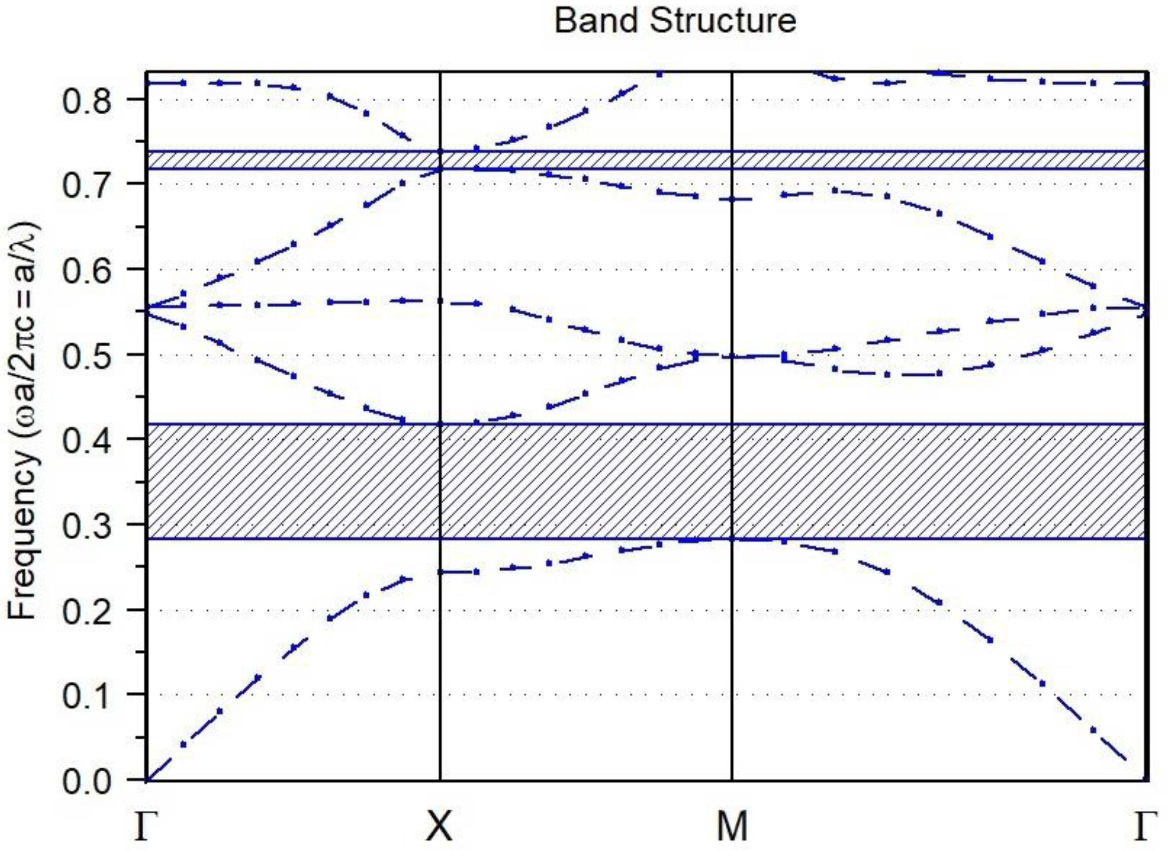
2. Design of Optical Comparator

We first selected a photonic crystal structure with a square lattice and a small size to design this comparator. Then we created waveguide paths using linear and point defects. That is, some rods in the waveguide paths were considered defective rods. To optimize the structure, we changed the defect rods’ radius and position. For the proposed design, simulations were performed for different values of the radius of the rods and their position. Then the obtained optimal state was given as the final structure.
A basic photonic crystal structure consisting of silicon rods with a circular cross-section in the air context was used to design the comparator. There were 24 × 19 rods that formed a two-dimensional square lattice, and the footprint of this structure was 149.04 µm2. The refractive index of the rods is 3.46, which was designed for approximately 1.55 µm wavelength. The lattice constant, which is the distance between the centers of the rods, was set to =0.6 µm for this structure. The radius of the silicon rods was also r = 0.2a.
This alternating structure led to creating an attribute called the photonic band gap (PBG). Based on this attribute, the propagation of a range of wavelengths in the structure was not allowed. The band structure calculations were also used to calculate this wavelength range. The plane wave expansion (PWE) method was used to calculate the band structure. Figure 1 depicts the results of the band structure calculations.
Figure 1 shows that the photonic crystal structure has two ranges of PBG. PBG is the range through which all of the wavelengths of the band cannot cross the crystal structure. In other words, these wavelengths are reflected after colliding with the structure. The light sources used must have a wavelength in the PBG range so that they can be propagated in the waveguide paths and propagated in the same path and not propagated in all parts of the structure.
As seen in Figure 1, no wavelength can enter the structure in the 0.28 to 0.42 normalized range. Since the normalized values are defined as a λ , the equivalent wavelength for this range is 1.42   μ m < λ < 2.14   μ m . Hence, this wavelength has to fall within the PGB range to select a suitable wavelength that can be controlled and directed in the structure. The 1.55 µm is selected as the operating wavelength, which is within the aforementioned range.
A combination of linear and point defects was used to obtain the optical comparator. The A and B inputs were placed on the top and bottom of the structure, and a constantly activated input called Ref was also placed on the left side of the structure. When both inputs were off, the output for their equality had to be activated; the Ref input served this purpose. Moreover, to improve the structure performance, reference Ref had a −70° phase shift in relation to the two input references. Three outputs were also selected for three possible states, which included A < B, A = B, and A > B. The outputs of these three states also included F1(A < B), F2(A = B), and F3(A > B). Figure 2 depicts the arrangement of the inputs and outputs and the link between their paths.
As seen in Figure 2, linear defects were used to obtain the comparator and create the input and output paths. These defects were created by omitting all of the rods. Point defects were also used at the intersection of the waveguide paths. The radius of the rods was changed for the point defects. Figure 2 shows the size of the radius of these rods. Some of the rods were also displaced as follows to improve comparator efficiency.
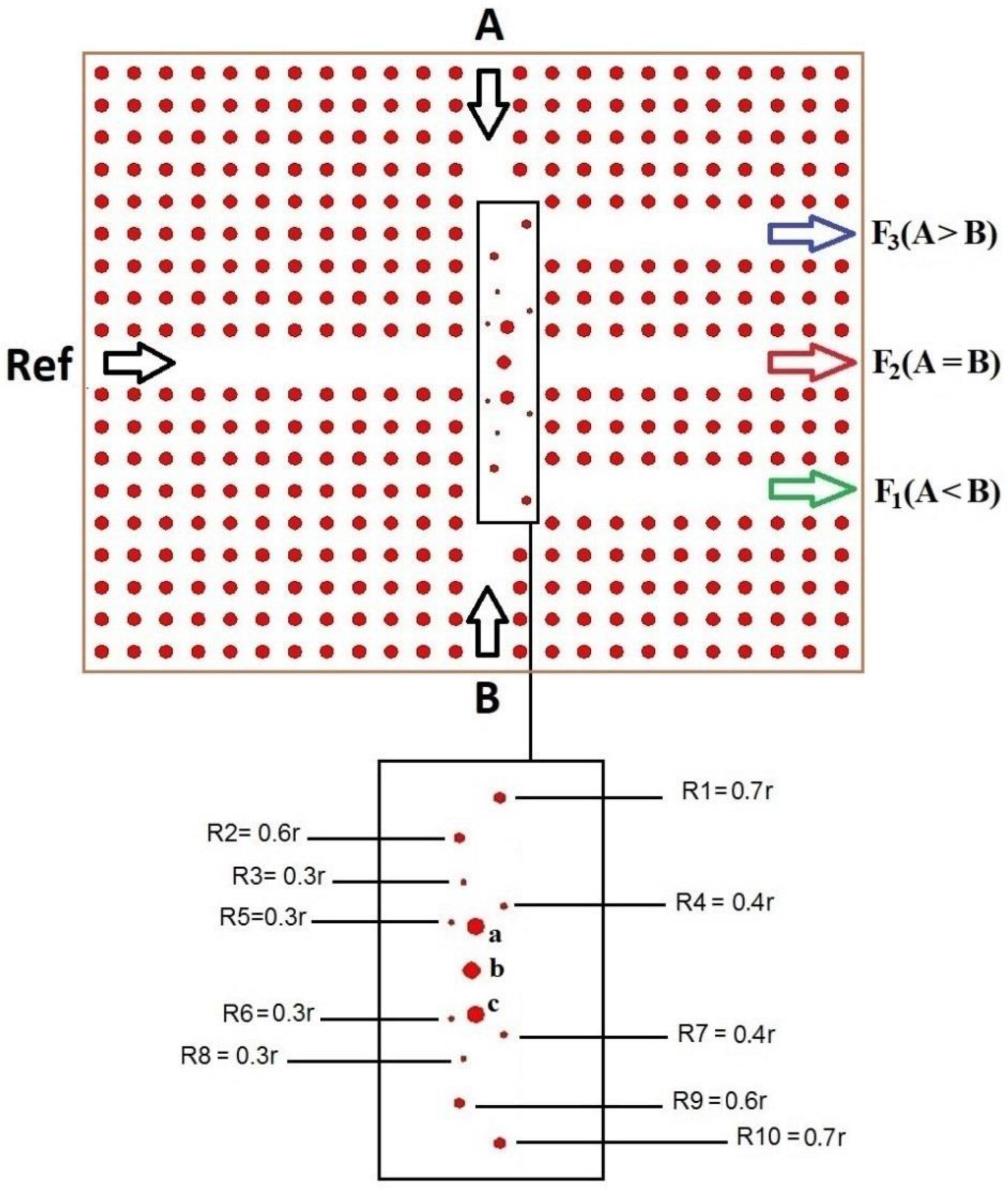
  • Rods with R1 and R2 radii: 0.2a rightward and 0.3a upward.
  • Rods with R3 radii: 0.3a rightward and 0.2a upward.
  • Rods with R4 radii: 0.3a rightward and 0.6a upward.
  • Rods with R5 radii: 0.2a upward.
  • Rods with R6 radii: 0.2a downward.
  • Rods with R7 radii: 0.3a rightward and 0.6a downward.
  • Rods with R8 radii: 0.3a rightward and 0.2a downward.
  • Rods with R9 and R10 radii: 0.2a rightward and 0.3a downward.
  • Rod a: 0.6a rightward and 0.1a upward.
  • Rod b: 0.5a rightward.
  • Rod c: 0.6a rightward and 0.1a downward.

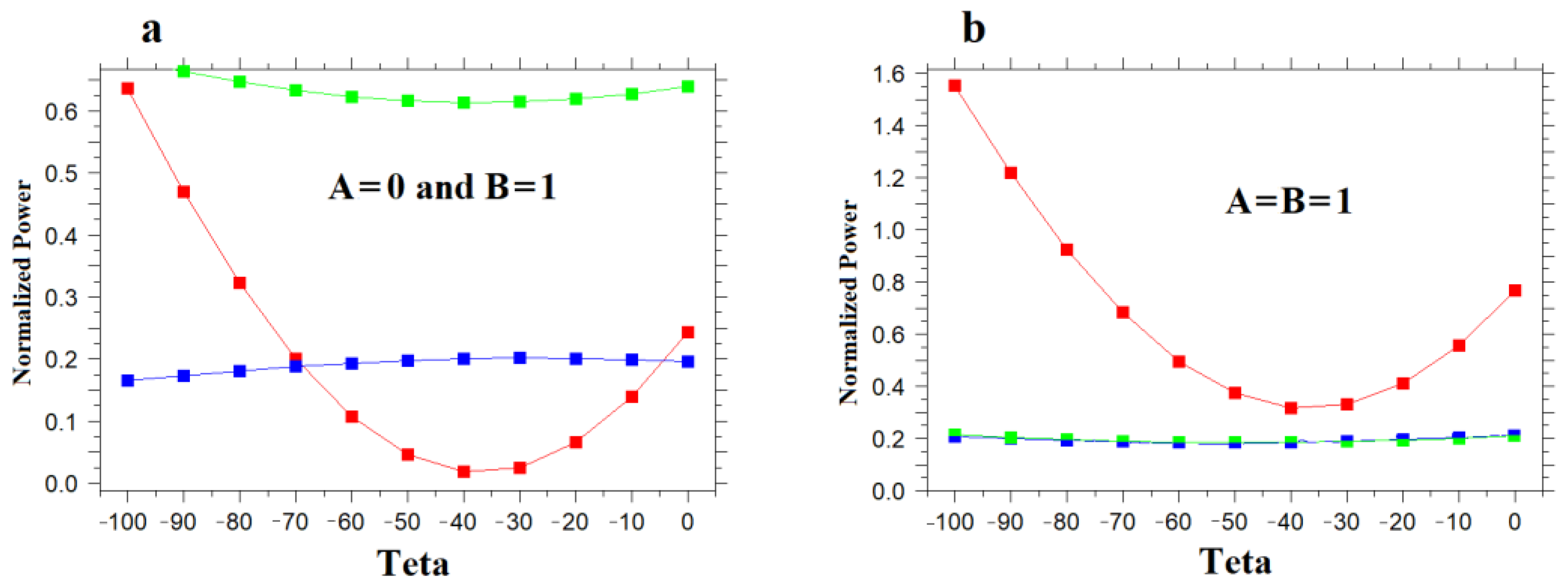
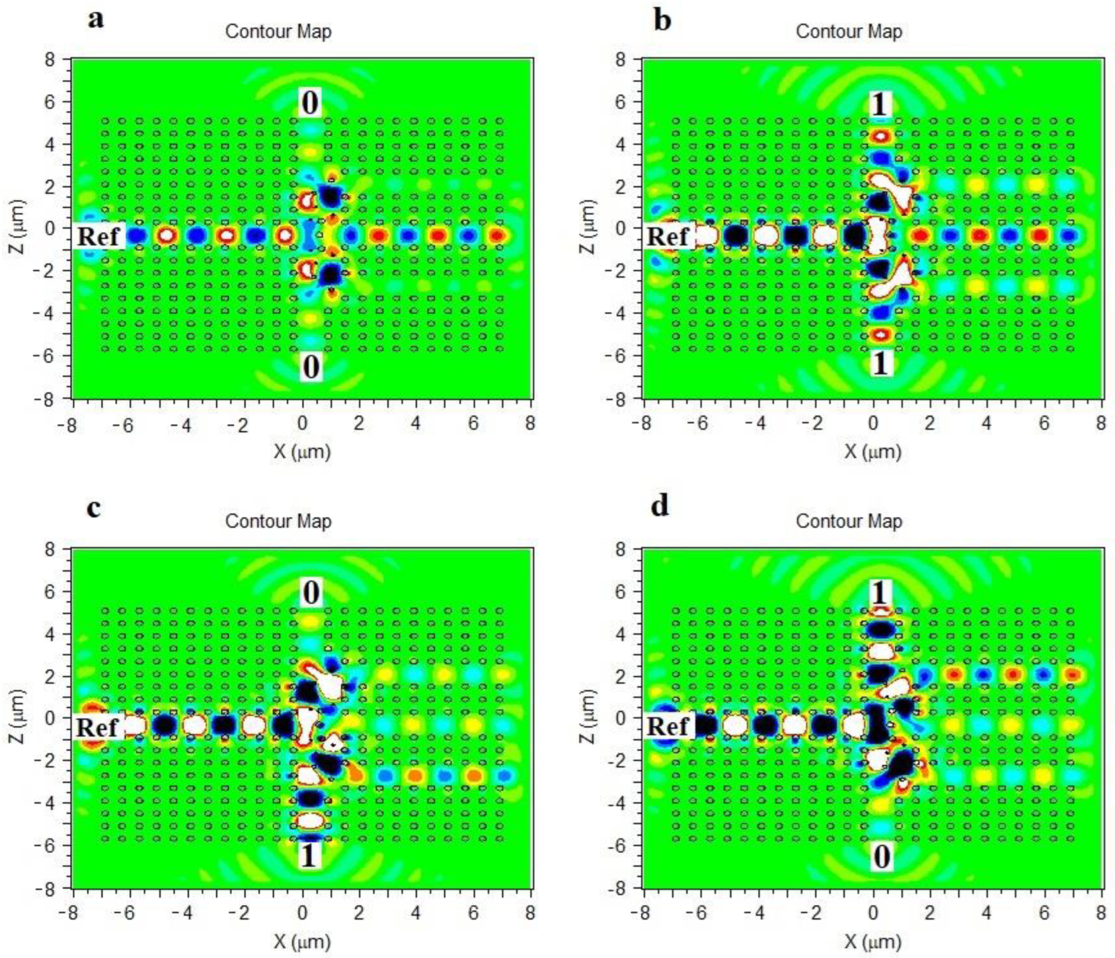
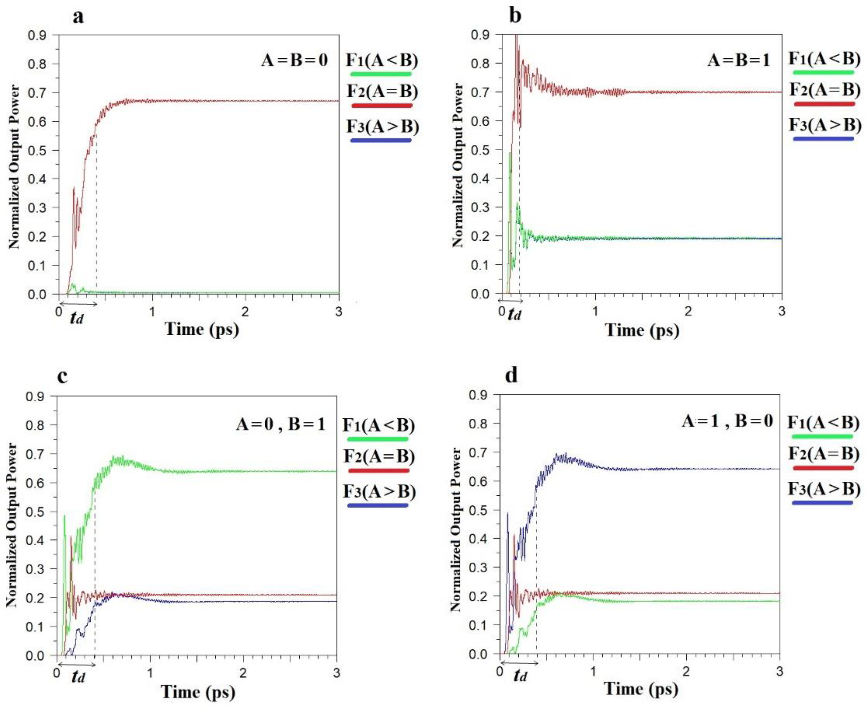
3. Simulation Results

As mentioned, to achieve the best outputs, the position and size of the defect rods were changed. Phase differences between incoming light waves can also be used to optimize the output response. We used simulations to achieve the best phase difference. Figure 3 shows the results of these simulations.
Figure 3 shows that if the Ref optical wave has a phase difference of −70 degrees relative to the input sources, the comparator will perform best. Due to the circuit symmetry, the A = 1 and B = 0 mode is the same as A = 0 and B = 1.
The comparator was simulated in four input states, and the optical power distribution in the structure was obtained in these states. Figure 4 shows the simulation results. Figure 4a shows power distribution for A = B = 0. As seen in this figure, the F2 output had considerable optical power, and it could be considered the equivalent to the logical value “1”. The optical power in the output was supplied by the reference (Ref) input source.
In this state, the decrease in power in the outputs is caused by the interference of the waves emitted from the inputs and Ref input at the intersection, while optimal power is only distributed along path F2 after colliding with the rods and the power level is very low in the other outputs. Figure 4b depicts the optical power distribution for A = B = 1. In this case, the output of F2 has a high power, and the other two outputs have a power close to zero.
Figure 4c shows the results when the inputs are A = 0, B = 1. Since in this state A < B, the F1 output is expected to be in the “1” state, and the other outputs are zero. As seen in this figure, the power distribution in the F1 output is significant and is equal to the logical value “1”.
If the inputs are A = 1, B = 0, i.e., A > B, the F3 output has to have high optical power, and other outputs have to have very low power due to the symmetry of the circuit. Figure 4d confirms this state. In other words, F3 equals logical value “1”, and the other outputs are in the “0” state.
Figure 5 presents the time curve of the variations of the optical power range in the comparator outputs. As seen in this figure, when A = B = 0, the normalized power in the F2 output equals 0.67, and power in the other two outputs equals 0.01. In other words, the F2 output equals the logical value “1. In addition, when A = B = 1, the power in the F2 output equals 0.70, while in other outputs, it is equal to 0.17. In other words, in this state, F2 equals the logical value “1” (see Figure 5a,b).
Figure 5c shows the normalized power diagram in the outputs of the comparator circuit for A = 0 and B = 1. In this state, the optical power in the F1 output is 0.66, which equals the logical value “1”. In the other two outputs, power equals 0.20, which equals the logical value “0”. The normalized power diagram for A = 1, B = 0 is also shown in Figure 5d. As seen in this figure, power in the F3 output, which has to be in the logical state “1”, equals 0.66, while in the other outputs, the optical power is low and equals 0.20.
As shown in Figure 5, in the worst case, the time required for the output to reach a steady state is less than 0.4 ps.
One of the important parameters in optical logic circuits is the contrast ratio (CR). This parameter is used to show the power difference in the two logic states, 0 and 1. This parameter is defined as CR = 10 log ( P 1 , min / P 0 , max ) where P1,min is minimum power in logic 1 and P0,max is maximum power in logic 0. In other words, the worst value is considered for all possible modes. According to Figure 5, this value can be calculated for all three outputs. For output F1 this value is equal to CR = 5.2 dB. Furthermore, for F2 and F3 outputs, these values are equal to 5.3 dB and 5.2 dB, respectively.
Delay time is another important parameter in digital circuits. If this time is defined as the time required for the output to reach 10% of the steady-state value, the delay times can be calculated for all four states shown in Figure 5. The delay time for A = B = 0 is 0.12 ps. This time for mode A = B = 1 is approximately equal to 0.1 ps. Moreover, in the case of A = 0, B = 1 this time is equal to 0.1 ps. Finally, the delay time at A = 1, B = 0 is approximately equal to 0.1 ps.
Several new articles were reviewed, and their results were compared to compare the proposed structure with previous studies. Table 1 shows the results of this comparison. It is worth noting that very few studies have been conducted on photonic crystal comparators. In Table 1, the size of this structure is compared to other papers. In addition, the worst value of each output in the “0” and “1” logical value states, i.e., the maximum power for “0” and the lowest power for “1”, are shown in this table and are compared to other structures.
As seen in Table 1, in references [28,29,30,31,33,34], the circuit size is large and does not suit the photonic integrated circuits despite the highly satisfactory “0” value. In reference [30], the values of “0” are not reported and the values of “1” are good logical values, but the circuit size is large. In reference [31], the logical value “0” is high, and the structure is also large. Finally, in reference [32], the structure is small, but two outputs are used simultaneously to compare the inputs. The value “1” in this circuit is also weak.
In these circuits [28,29,30,31,32,33,34], the logical values (“0” and “1”) and the structure size are not optimized, but in our proposed comparator, the circuit size is small, while the high difference between the two logical values is also taken into account. It can also be seen that the rise time is very low in the proposed structure and can be used in high-speed optical integrated circuits. Another feature of this structure is the simplicity of designing and using very few waveguides. Furthermore, no nonlinear rods are used in this structure, and all rods are homogeneous. In addition, only one control source has been used in the design of this structure. These features make its design and fabrication easier.

4. Conclusions

In this study, a one-bit comparator is designed and simulated. This circuit can compare two input bits and put one of the three outputs in the logical state “1”. One of the characteristics of the designed structure is its small size, which makes the comparator suitable for photonic integrated circuits. Moreover, the distance between two logical values is considered in designing the comparator to ensure the distance is relatively good. Another characteristic of this circuit is its simple design, which involves simple linear and point defects and does not include resonators that increase the circuit delay time.

Author Contributions

F.P. supervised, R.K. designed and performed simulations, M.J. analyzed data, S.O. edited and prepared the final draft of the manuscript. All authors have read and agreed to the published version of the manuscript.

Funding

This research received no external funding.

Institutional Review Board Statement

Not applicable.

Informed Consent Statement

Not applicable.

Data Availability Statement

Not applicable.

Acknowledgments

This work was undertaken in the Department of Electrical Engineering, Kermanshah Branch, Islamic Azad University and Nano-photonics and Optoelectronics Research Laboratory (NORLab), Shahid Rajaee University.

Conflicts of Interest

The authors declare that they have no known competing financial interests or personal relationships that could have appeared to influence the work reported in this paper.

References

  1. Lalbakhsh, A.; Afzal, M.U.; Hayat, T.; Esselle, K.P.; Mandal, K. All-metal wideband metasurface for near-field transformation of medium-to-high gain electromagnetic sources. Sci. Rep. 2021, 11, 9421. [Google Scholar] [CrossRef] [PubMed]
  2. Lalbakhsh, A.; Mohamadpour, G.; Roshani, S.; Ami, M.; Roshani, S.; Sayem, A.S.M.; Alibakhshikenari, M.; Koziel, S. Design of a Compact Planar Transmission Line for Miniaturized Rat-Race Coupler With Harmonics Suppression. IEEE Access 2021, 9, 129207–129217. [Google Scholar] [CrossRef]
  3. Hadei, M.; Dadashzadeh, G.; Torabi, Y.; Lalbakhsh, A. Terahertz beamforming network with a nonuniform contour. Appl. Opt. 2022, 61, 1087–1096. [Google Scholar] [CrossRef] [PubMed]
  4. Roshani, S.; Roshani, S. Design of a high efficiency class-F power amplifier with large signal and small signal measurements. Measurement 2020, 149, 106991. [Google Scholar] [CrossRef]
  5. John, S. Strong localization of photons in certain disordered dielectric superlattices. Phys. Rev. Lett. 1987, 58, 2486–2489. [Google Scholar] [CrossRef] [PubMed] [Green Version]
  6. Parandin, F.; Mahtabi, N. Design of an ultra-compact and high-contrast ratio all-optical NOR gate. Opt. Quantum Electron. 2021, 53, 666. [Google Scholar] [CrossRef]
  7. Fan, S.; Yanik, M.F.; Wang, Z.; Sandhu, S.; Povinelli, M.L. Advances in Theory of Photonic Crystals. J. Lightwave Technol. 2006, 24, 4493–4501. [Google Scholar] [CrossRef]
  8. Parandin, F. Ultra-compact terahertz all-optical logic comparator on GaAs photonic crystal platform. Opt. Laser Technol. 2021, 144, 107399. [Google Scholar] [CrossRef]
  9. Parandin, F.; Kamarian, R.; Jomour, M. Optical 1-bit comparator based on two-dimensional photonic crystals. Appl. Opt. 2021, 60, 2275–2280. [Google Scholar] [CrossRef]
  10. Parandin, F.; Heidari, F.; Rahimi, Z.; Olyaee, S. Two-Dimensional photonic crystal Biosensors: A review. Opt. Laser Technol. 2021, 144, 107397. [Google Scholar] [CrossRef]
  11. Miri, M.; Sodagar, M.; Mehrany, K.; Eftekhar, A.A.; Adibi, A.; Rashidian, B. Design and Fabrication of Photonic Crystal Nano-Beam Resonator: Transmission Line Model. J. Lightwave Technol. 2013, 32, 91–98. [Google Scholar] [CrossRef]
  12. Gupta, M.M.; Medhekar, S. All-optical NOT and AND gates using counter propagating beams innonlinear Mach–Zehnder interferometer made of photonic crystal waveguides. Optik 2016, 127, 1221–1228. [Google Scholar] [CrossRef]
  13. Parandin, F. Realization of Ultra-compact All-optical Universal NOR Gate on Photonic Crystal Platform. J. Electr. Comput. Eng. Innov. 2021, 9, 185–192. [Google Scholar]
  14. Farmani, A.; Mir, A.; Irannejad, M. 2D-FDTD simulation of ultra-compact multifunctional logic gates with nonlinear photonic crystal. J. Opt. Soc. Am. B 2019, 36, 811–818. [Google Scholar] [CrossRef]
  15. Parandin, F.; Sheykhian, A. Design and simulation of a 2 × 1 All-Optical multiplexer based on photonic crystals. Opt. Laser Technol. 2022, 151, 108021. [Google Scholar] [CrossRef]
  16. Ghadrdan, M.; Mansouri-Birjandi, M.A. Concurrent implementation of all-optical half-adder and AND & XOR logic gates based on nonlinear photonic crystal. Opt. Quantum Electron. 2013, 45, 1027–1036. [Google Scholar]
  17. Parandin, F.; Moayed, M. Designing and simulation of 3-input majority gate based on two-dimensional photonic crystals. Optik 2020, 216, 164930. [Google Scholar] [CrossRef]
  18. Gilarlue, M.; Badri, S.H. Photonic crystal waveguide crossing based on transformation optics. Opt. Commun. 2019, 450, 308–315. [Google Scholar] [CrossRef] [Green Version]
  19. Parandin, F. High contrast ratio all-optical 4 × 2 encoder based on two-dimensional photonic crystals. Opt. Laser Technol. 2019, 113, 447–452. [Google Scholar] [CrossRef]
  20. Neisy, M.; Soroosh, M.; Ansari-Asl, K. All optical half adder based on photonic crystal resonant cavities. Photonic Netw. Commun. 2018, 35, 245–250. [Google Scholar] [CrossRef]
  21. Moniem, T.A. All-optical digital 4 × 2 encoder based on 2D photonic crystal ring resonators. J. Mod. Opt. 2015, 63, 735–741. [Google Scholar] [CrossRef]
  22. Naghizade, S.; Saghaei, H. A novel design of all-optical 4 to 2 encoder with multiple defects in silica-based photonic crystal fiber. Optik 2020, 222, 165419. [Google Scholar] [CrossRef]
  23. Sani, M.H.; Tabrizi, A.A.; Saghaei, H.; Karimzadeh, R. An ultrafast all-optical half adder using nonlinear ring resonators in photonic crystal microstructure. Opt. Quantum Electron. 2020, 52, 107. [Google Scholar] [CrossRef]
  24. Naghizade, S.; Saghaei, H. A novel design of all-optical half adder using a linear defect in a square lattice rod-based photonic crystal microstructure. arXiv 2020, arXiv:2002.04535. [Google Scholar]
  25. Naghizade, S.; Mohammadi, S.; Khoshsima, H. Design and simulation of an all optical 8 to 3 binary encoder based on optimized photonic crystal OR gates. J. Opt. Commun. 2018, 42, 31–41. [Google Scholar] [CrossRef]
  26. Parandin, F.; Kamarian, R.; Jomour, M. A novel design of all optical half-subtractor using a square lattice photonic crystals. Opt. Quantum Electron. 2021, 53, 114. [Google Scholar] [CrossRef]
  27. Rathi, S.; Swarnakar, S.; Kumar, S. Design of One-Bit Magnitude Comparator using Photonic Crystals. J. Opt. Commun. 2019, 40, 363–367. [Google Scholar] [CrossRef]
  28. Fakouri-Farid, V.; Andalib, A. Design and simulation of an all optical photonic crystal-based comparator. Optik 2018, 172, 241–248. [Google Scholar] [CrossRef]
  29. Serajmohammadi, S.; Alipour-Banaei, H.; Mehdizadeh, F. A novel proposal for all optical 1-bit comparator using nonlinear PhCRRs. Photonics-Nanostruct.-Fundam. Appl. 2019, 34, 19–23. [Google Scholar] [CrossRef]
  30. Surendar, A.; Asghari, M.; Mehdizadeh, F. A novel proposal for all-optical 1-bit comparator using nonlinear PhCRRs. Photonics-Netw. Commun. 2019, 38, 244–249. [Google Scholar] [CrossRef]
  31. Jalali, S.M.; Soroosh, M.; Akbarizadeh, G. Ultra-fast 1-bit comparator using nonlinear photonic crystalbased ring resonators. J. Optoelectron. Nanostruct. 2019, 4, 59–72. [Google Scholar]
  32. Seraj, Z.; Soroosh, M.; Alaei-Sheini, N. Ultra-compact ultra-fast 1-bit comparator based on a two-dimensional nonlinear photonic crystal structure. Appl. Opt. 2020, 59, 811–816. [Google Scholar] [CrossRef] [PubMed]
  33. Zhu, L.; Mehdizadeh, F.; Talebzadeh, R. Application of photonic-crystal-based nonlinear ring resonators for realizing an all-optical comparator. Appl. Opt. 2019, 58, 8316–8321. [Google Scholar] [CrossRef] [PubMed]
  34. Jile, H. Realization of an all-optical comparator using beam interference inside photonic crystal waveguides. Appl. Opt. 2020, 59, 3714–3719. [Google Scholar] [CrossRef]
Figure 1. PBG range for the basic structure.
Photonics 09 00459 g001
Figure 2. The proposed optical comparator structure.
Photonics 09 00459 g002
Figure 3. Diagram of output power changes in terms of phase difference changes (a) A B and (b) A = B = 1.
Photonics 09 00459 g003
Figure 4. The optical power distribution of the comparator in different input states. (a) A = B = 0, (b) A = B = 1, (c) A = 0 and B = 1, (d) A = 1 and B = 0.
Photonics 09 00459 g004
Figure 5. The normalized power diagram in the comparator outputs for different input states. (a) A = B = 0, (b) A = B = 1, (c) A = 0 and B = 1, (d) A = 1 and B = 0.
Photonics 09 00459 g005
Table 1. Comparison the proposed comparator with other works.
ReferencesSizeF1
“1”Min Power
F1
“0”Max Power
F2
“1”Min Power
F2
“0”Max Power
F3
“1”Min Power
F3
“0”Max Power
Rise Time (ps)
[28]86 × 490.850.060.850.080.900.053.0
[29]100 × 741.40.050.800.0010.053.0
[30]65 × 310.91-0.90-0.83-1.5
[31]121 × 370.710.100.890.200.750.252.5
[32]13 × 130.47--0.110.800.140.31
[33]80 × 410.880.080.750.040.780.031.5
[34]77 × 1110.900.200.900.200.980.020.6
This Work24 × 190.660.200.670.20.660.200.4
Publisher’s Note: MDPI stays neutral with regard to jurisdictional claims in published maps and institutional affiliations.

