Article

Improving the Performance of Direct Bonded Five-Junction Solar Cells by Optimization of AlInP Window Layer

1
State Key Laboratory of Space Power-Sources, Shanghai 200245, China
2
Shanghai Institute of Space Power-Sources, Shanghai 200245, China
*
Author to whom correspondence should be addressed.
Photonics 2022, 9(6), 404; https://doi.org/10.3390/photonics9060404
Submission received: 30 April 2022 / Revised: 2 June 2022 / Accepted: 3 June 2022 / Published: 8 June 2022
(This article belongs to the Special Issue Recent Progress in Solar Cell Technology and Future Prospects)

Abstract

:
It is well-known that the quantum efficiency (QE) of inverted AlGaInP solar cells is less than that of upright ones, and the mechanism has not been well-explained. In this paper, a Si-doped AlInP window layer, compared with an emitter layer, is revealed to be one more important factor that decreases QE. It is noted that the quality of a heavily Si-doped AlInP window layer would decrease and further deteriorate subsequent active layers. An optimization strategy of a Si-doped AlInP window layer is proposed, which proves effective through time-resolved photoluminescence measurements (TRPL) of double heterojunctions. Inverted 2.1 eV AlGaInP solar cells with an improved AlInP window layer are fabricated. A 60 mV Voc increment is achieved with a remarkable enhancement of the fill factor from 0.789 to 0.827. An enhanced QE of 10% to 20% is achieved at short-wavelength and the peak IQE rises from 83.3% to 88.2%, which presents a nearly identical IQE compared with the upright reference. Further optimization in GaAs homojunction sub-cells is performed by introducing an n-GaInP/p-GaAs heterojunction structure, which decreases the recombination loss in the emitter caused by a poor AlInP window layer. The optimized structure significantly improves the Voc of the inverted GaAs-based T-3J solar cells to 3830 mV, boosting the efficiency of SBT five-junction solar cells to 35.61% under AM0 illumination.

1. Introduction

III-V multi-junction solar cells continue to lead the development of solar cells with the highest efficiency, which depends on the optimal bandgap combination and the realizability of the designed structure [1,2,3,4,5,6,7]. The rapid progress in epitaxial and device technology makes the efficiency of single-, dual- and triple-junction solar cells approach their theoretical maximum values [8,9]. Breakthroughs in efficiency can be made in four-junction or greater solar cells, which further improves the utilization of photon energy.
Among various multi-junction solar cell fabrication roadmaps, the semiconductor direct bonding technique (SBT) has been demonstrated to have great potential in developing larger-area and higher-efficiency solar cells [6], which has created the highest conversion efficiency (36%) under the AM0 space spectrum up to now. Based on the detailed balance model, the SBT five-junction solar cell with a 2.10/1.70/1.42//1.1/0.8 eV bandgap combination in AM0 spectrum can realize an efficiency of >36%, considering the actual device process loss factor of 15% [10]. This SBT five-junction solar cell is usually composed of an upright bottom two-junction sub-cell (B-2J) lattice-matched to InP and an inverted top three-junction sub-cell (T-3J) lattice-matched to GaAs [7]. The final five-junction solar cell efficiency is limited by the performance of these two sub-cells and the electrical loss at the bonding interface [10].
Further, 2.1 eV AlGaInP solar cells with an Al-content over 18% have been employed as the top cell of five-junction solar cells for the highest direct bandgap among III-V semiconductors lattice-matched to GaAs. It is widely recognized that high-Al-content AlGaInP quaternary alloys face more epitaxy difficulty. Upright 2.05 eV AlGaInP solar cells grown by metal organic vaper phase epitaxy (MOVPE) with a Voc of 1457 mV were fabricated for the multi-junction structure [11]. Molecular-beam-epitaxy (MBE)-grown 2.1 eV AlGaInP solar cells were treated with the RTA process and achieved a Voc of 1505 mV [12]. To further reduce defects in high-Al-content material, a high growth temperature was processed in AlGaInP solar cells and a Voc of 1590 mV could be achieved in the 2.1 eV AlGaInP solar cells [13]. Recently, a new structure called a reverse heterojunction AlGaInP solar cell has been proposed to relieve the problem [14]. Although the carrier collection efficiency is enhanced due to a lower defect concentration in the emitter layer, the reduced Voc and problem of current-match in multi-junction solar cells limit the application of this structure. However, the solar cell designed above is an upright structure and could hardly be used in four-junction or greater solar cells. Performance degradation in inverted AlGaInP solar cells would cause reduced carrier collection efficiency and make the AlGaInP top-cell the current-limiting sub-cell [12,15,16].
This paper focuses on the optimization of inverted GaAs T-3J sub-cells. Through comparative experiments, the key factors restricting the T-3J performance are analyzed. Improvements through structure design and epitaxial growth process are proposed and realized. The open circuit voltage (Voc) of the inverted GaAs T-3J sub-cell eventually increases from ~3710 mV to ~3830 mV. A high Voc is achieved and a better current-match condition realized, which help to boost the efficiency of SBT five-junction solar cells to 35.61%.

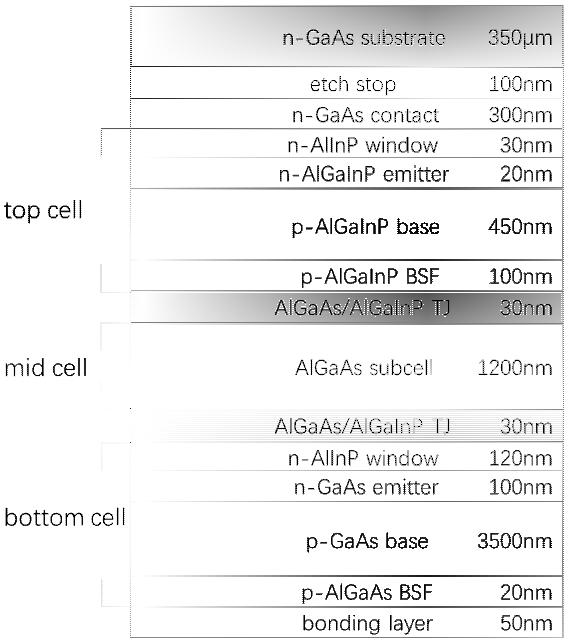
2. Materials and Methods

All III-V solar cells and related samples were grown using an AIX-2600 G3 MOCVD installation. The primary group III and group V precursors used were trimethylgallium (TMGa), trimethylindium (TMIn), trimethylaluminium (TMAl), arsine (AsH3) and phosphine (PH3). The dopant precursors used were silane (SiH4), trimethyltellurium (DETe), carbon tetrabromide (CBr4) and diethylzinc (DEZn). The V/III ratio of all epilayers was maintained at 250–300. Chamber pressure was set to 100 mbar, and 4-inch n-type 15° off-cut (001) epi-ready GaAs substrates (purchased from Vital Inc., Tokyo, Japan) were used for T-3J solar cells, while 3-inch n-type and p-type 0° off-cut (001) epi-ready InP substrates (purchased from Vital Inc.) were used for B-2J solar cells.
Figure 1 illustrated typical schematic cross-section structure of the inverted T-3J solar cell device, which is lattice-matched to GaAs substrate. The active region of each sub-cell consists of n-on-p junction (emitter/base) surrounded by n-type window layer and p-type BSF layer. Detailed T-3J structure could be seen in Figure S1. High-performance AlGaInP/AlGaAs tunnel junctions were used to connect sub-cells, which were optically transparent to the underlying sub-cells and achieved a tunneling current density of over 7.8 A/cm2 [17]. After growth process, epi-layers were transferred to InP substrates or InP-based dual-junction solar cells through direct bonding technique [7,18]. Following the direct bonding, GaAs substrates were removed. Photolithography techniques were utilized for the fabrication of the devices. Pd/Zn/PdAu stacks were deposited on substrates backside and annealed to provide ohmic contacts. AuGeNi/Au/Ag/Au stacks were deposited on contact layer as front grids. The structures were processed following standard III-V solar cell device art. Finally, wafers were cut into cells in size of 2.0 × 2.0 cm2 (Figure S2). Details of device process have been described previously [10,19].
The light J–V measurements were performed under Spectrolab X-25A AM0 simulator. External quantum efficiency (EQE) and reflectance (R) were evaluated using an EnLi apparatus. Then, internal quantum efficiency (IQE) was calculated through EQE/(1-R). Cells were placed on 25 °C cooled stage during the measurements. The doping concentration of epi-layers was measured through electrochemical capacitance–voltage method (Nanometric-ECVPro). Double heterojunctions (DH) with 2.1 eV AlGaInP embedded between Si-doped AlInP barriers were grown to evaluate the carrier recombination. Time-resolved photoluminescence measurements (TRPL) were performed at room temperature to evaluate the carrier lifetime using the time correlated single photon counting technique. The excitation wavelength was 532 nm, and all samples were in low-level injection conditions.

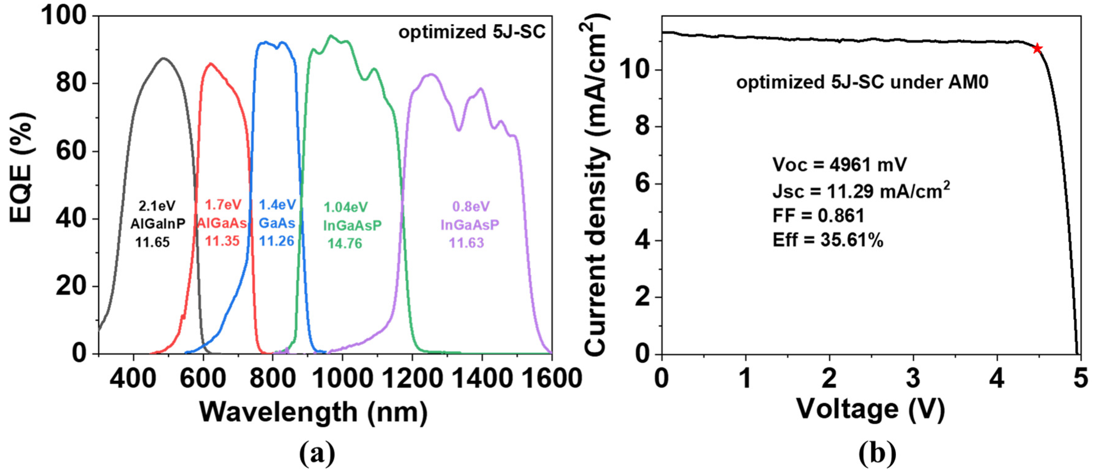
3. Results and Discussion

3.1. Epitaxy Process Optimization in AlGaInP Sub-Cell

As shown in Figure 2, the upright and inverted AlGaInP/AlGaAs/GaAs three-junction solar cells made of an identical structure are fabricated and measured, which show the same pattern as reported previously [12,15,16]. The IQE of the 1.7 eV AlGaAs sub-cell remains nearly unchanged, which indicates that the AlGaAs growth direction has little effect on the device performance. However, the IQE of the inverted 2.1 eV AlGaInP top-cell decreases by 10% to 20% compared with the upright reference in the range of 300 to 500 nm. The calculated current density from the integral of the IQE curve could be acquired to estimate the current-match condition of the T-3J solar cells. For the upright T-3J solar cell, the integral current density of the AlGaInP, AlGaAs and GaAs sub-cell is 12.49 mA/cm2, 11.58 mA/cm2 and 11.59 mA/cm2, respectively. However, the integral current density of the AlGaInP sub-cell in the inverted solar cells decreases to 11.09 mA/cm2. The reduced carrier collection efficiency in the AlGaInP sub-cell causes current-mismatch and makes the AlGaInP sub-cell current-limiting, which would affect the performance of multi-junction solar cells.
For solar cell devices, such a reduction in the IQE means poor carrier collection efficiency and is mostly caused by the short minority carrier diffusion length in the base or emitter, which is the result of an inappropriate thickness or doping concentration [13]. It is widely recognized that AlInP or AlGaInP compounds with high Al contents will introduce more defects, such as Al-O defects [20,21,22], Si-related DX centers [23,24] and P-vacancies [25]. Defects in solar cells have been characterized and modeled using DLTS measurement [26,27,28], which should be controlled in high-efficiency solar cells. Usually, compared with GaInP, high-Al-content compounds are grown at a higher temperature and V/III ratio to decrease O-related defects and P-vacancies-related defects, respectively [13]. Si-related DX centers tend to grow with increasing Al-content and eventually reduce solar cell performance [12,20,23,29]. However, since the architecture of both upright and inverted devices remains the same, it is hard to explain the differences in IQE.

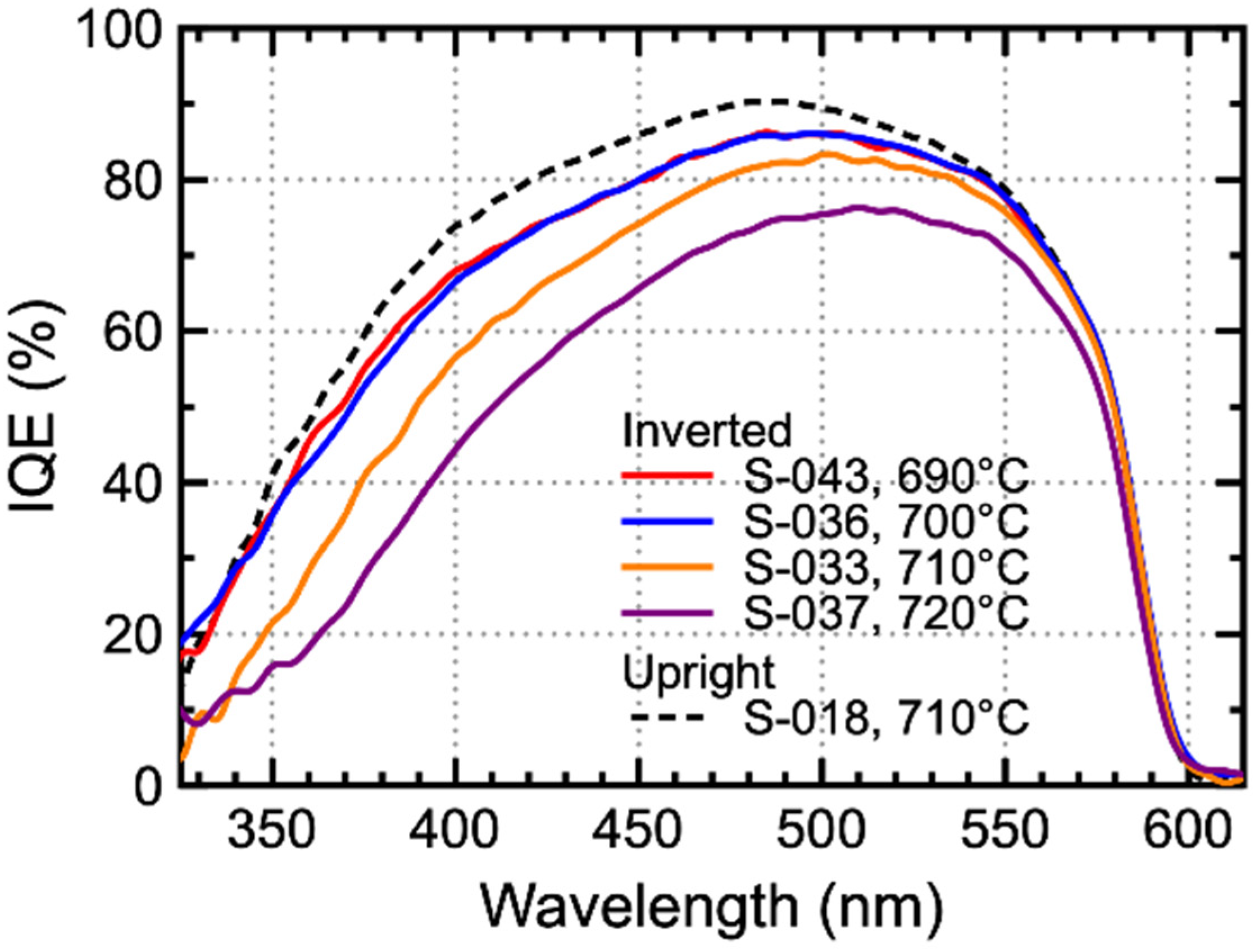
3.1.1. Effect of Growth Temperature

First, the influence of the growth temperature of inverted AlGaInP solar cells is investigated. Since AlGaAs sub-cells grown in different directions (upright and inverted structure) make no difference to the IQE performance, as shown in Figure 2, AlGaInP/AlGaAs dual-junction solar cells are used in this paper for a tradeoff between optical environment and process complexity [19]. As shown in Figure S3, the AlGaAs absorbing layer is 400 nm thicker than the designed AlGaAs sub-cell in the T-3J structure to generate enough photocurrent and make the AlGaInP sub-cell current-limiting. Figure 3 depicts the IQE of inverted AlGaInP sub-cells grown at increasing temperature from 690 °C to 720 °C (S-043, S-036, S-033 and S-037), together with the IQE of the upright AlGaInP sub-cell grown at 710 °C (S-018) as a benchmark (dashed line). It is obvious that the IQE values of all the inverted solar cells are lower than that of the upright one. For inverted AlGaInP solar cells grown at 690 °C, 700 °C, 710 °C and 720 °C, the peak IQE is 86.3%, 86.0%, 83.1% and 76.3%, respectively. Obviously, there is a remarkable reduction in the IQE as the growth temperature elevates, although the difference between the solar cells grown at 690 °C (S-043) and 700 °C (S-036) is minor. Besides the decreased IQE, the open-circuit voltage (Voc) of inverted AlGaInP/AlGaAs dual-junction solar cells decreases as the growth temperature increases, as shown in Table 1. Considering the minor differences between upright and inverted AlGaAs sub-cells, it is reasonable to attribute the decrease in Voc to the degradation of AlGaInP sub-cells. The Voc loss of the inverted AlGaInP solar cells grown at 690 °C, 700 °C, 710 °C and 720 °C could be roughly estimated to be 49 mV, 98 mV, 101 mV and 130 mV, respectively, compared with the upright AlGaInP solar cell (S-018).
High-Al-content upright AlGaInP solar cells grown at higher temperatures are supposed to have better performance [13,22,30]. However, the IQE curves of the inverted solar cells in Figure 3 indicate the opposite results. As the temperature increases, the collection efficiency of the inverted AlGaInP solar cell tends to decrease significantly. The drop in the IQE mainly originates from the poor short-wavelength response. According to Hovel’s model [31], reduced collection efficiency in short-wavelength range is mostly caused by the topmost layers in the solar cell, namely the emitter and window layer. The minority carrier diffusion length in the emitter (Lp) and interface recombination velocity between the emitter and window layer might influence the short-wavelength IQE. Both parameters are relevant to the doping levels of the emitter and window layer. Since the mole flows of the dopants are fixed during the growth of the above sub-cells, in spite of varied temperatures, such degradation might be related to increased defects and Si-related DX centers as a result of increased Si dopant incorporation at an elevated temperature for high-Al-content AlGaInP [24,32].

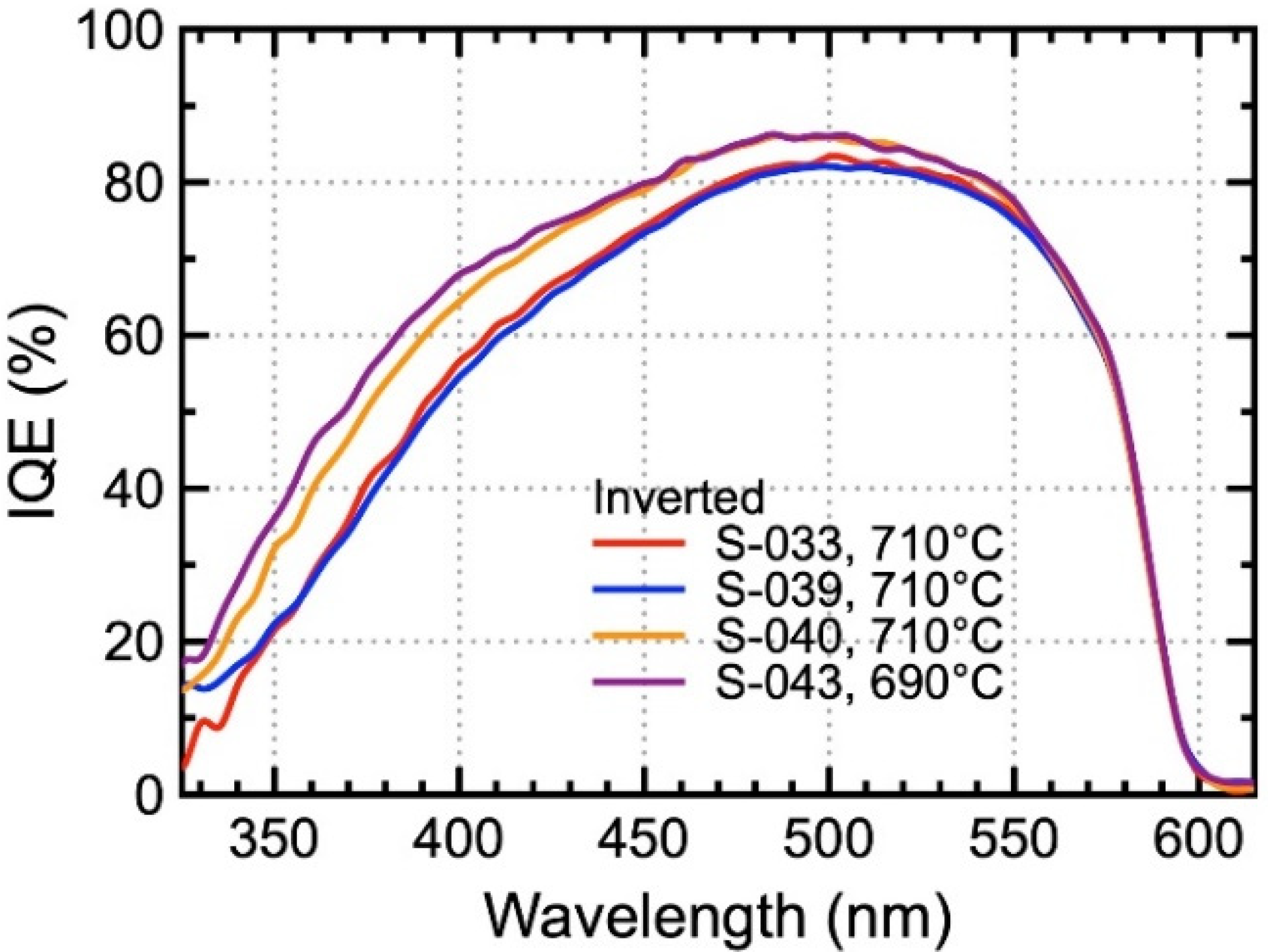
3.1.2. Effect of Doping Concentration

To investigate the influence of the Si dopant concentration, solar cells with reduced doping levels in the window and emitter layers, as shown in Table 2, are then fabricated. The IQE curves of AlGaInP sub-cells with different Si doping concentrations are displayed in Figure 4.
First, the influence of a Si-doped AlGaInP emitter layer with different dopant concentrations is considered. A lower doping level by one order of magnitude in the Si-doped emitter layer of S-039 (3 × 1017 cm−3) compared to that of S-033 (3 × 1018 cm−3) results in a Voc loss of about 60 mV, which could be estimated by the built-in voltage in equilibrium (Vbi) caused by the lower emitter concentration. The reduced emitter concentration would result in a longer minority carrier lifetime in the emitter and less recombination loss. However, the IQE curve of S-039 remains almost the same as that of S-033, which suggests that the carrier collection efficiency is not dominated by the emitter layer.
Then, the impact of the doping level in the window layer is considered and analyzed. S-040 (7 × 1017 cm−3) with a further reduced doping level of the Si-doped AlInP window layer is fabricated and compared with S-039 (7 × 1018 cm−3). The Voc values of S-039 and S-040 are almost the same, which could be attributed to the identical doping level in the emitter. The poor FF of S-040 is greatly degraded due to a high barrier for the majority carrier across the interface between the window and emitter caused by the decreased doping concentration in the window. In particular, the IQE presents an appreciable recovery from the poor short-wavelength response and is enhanced by 10% to 20%, which means that the window layer plays a more dominating role in the short-wavelength response of the inverted AlGaInP solar cells than the emitter layer. It seems that the lower doping level in the Si-doped AlInP window layer might improve the IQE performance, which is rather counter-intuitive. According to the traditional Hovel’s model [31,33], the doping concentration in the window layer has little direct impact on the carrier collection efficiency. In addition, the solar cells fabricated in this paper possess a front-emitter structure with nearly all depleted emitters. The change in the interface recombination velocity only slightly contributes to the total collection efficiency. Thus, it suggests that the improved carrier collection efficiency comes from the recovered minority carrier diffusion length in the emitter layer. The Si doping concentration of the window layer might play an important role in the minority carrier transport process.
However, S-043 (690 °C) with a high doping level in the window layer (6 × 1018 cm−3) shows even a slightly improved IQE compared with S-040 (710 °C). At 690 °C, higher Si-doped in the AlInP window layer seems to have little effect on the material quality of the active layer. It proposes that a reduction in the IQE is not simply caused by the Si doping level in the window layer. The growth temperature of the window layer, besides the doping level, will also result in a reduction in the solar cell performance directly.

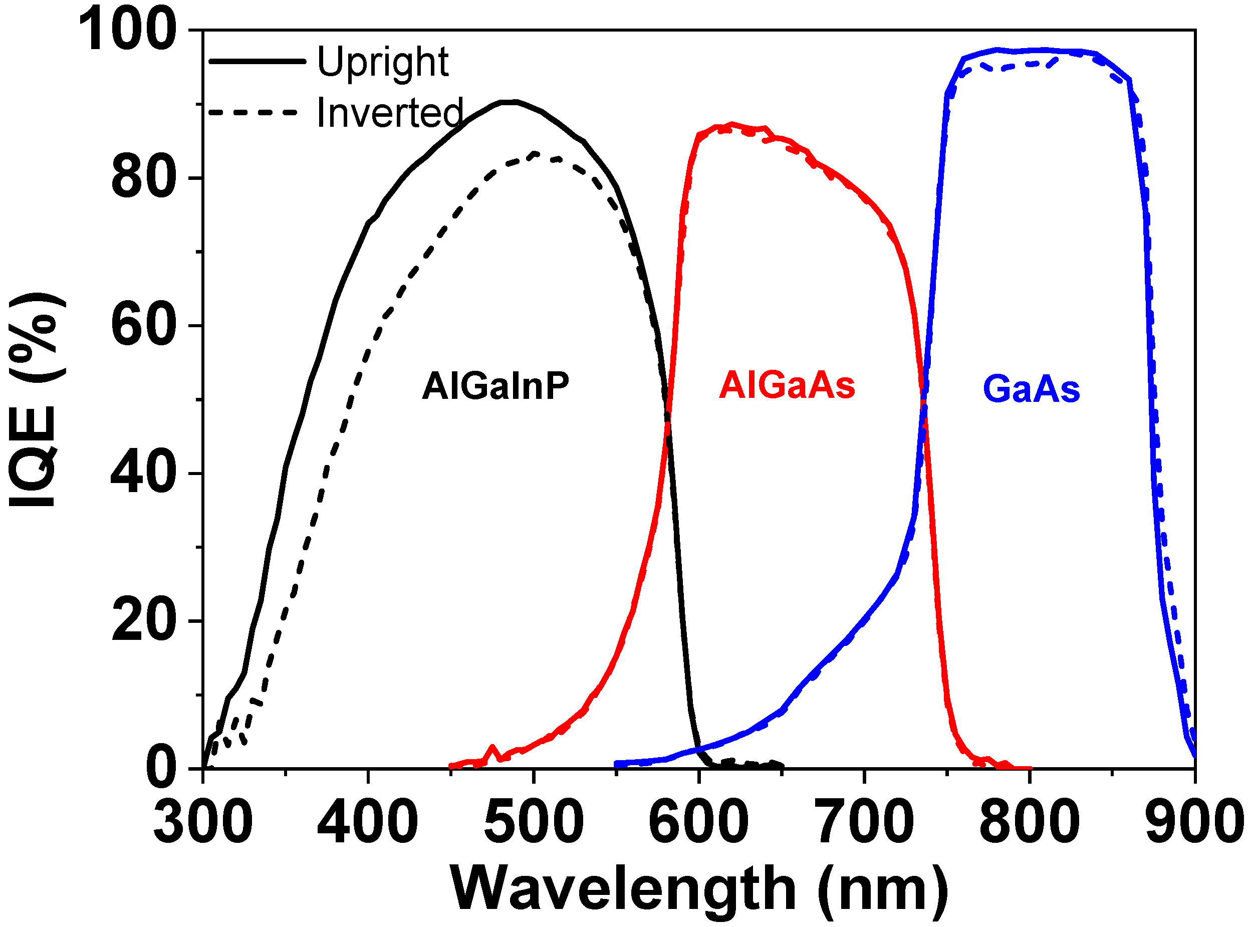
3.1.3. Effect of Window Verified by 2.1 eV AlGaInP DHs

AlInP/AlGaInP DHs are employed to determine the impact of the AlInP window layer on the 2.1 eV Al0.18Ga0.33In0.49P bulk layer. The DH consists of a 500 nm Si-doped 2.1 eV Al0.18Ga0.33In0.49P bulk layer, which is embedded between a 100 nm Si-doped AlInP barrier. Besides the samples grown at 690 °C and 710 °C, another temperature-shift-grown DH, meaning a 2.1 eV AlGaInP layer grown at 710 °C and AlInP barrier grown at 690 °C, is prepared. Growth pauses of 120 s are introduced at both interfaces to ramp up or down the temperature, with a moderate PH3 inlet to stabilize the growth surface. In addition, all three DHs (710 °C/710 °C, 690 °C/690 °C and 690 °C/710 °C) have the same growth pause between the AlInP barrier and AlGaInP bulk layer to keep the interface conditions identical. The doping concentrations of the Si-doped AlInP barriers are the same as those in the AlGaInP sub-cells grown at different temperatures (7 × 1018 cm−3 for 710 °C and 6 × 1018 cm−3 for 690 °C).
Figure 5 displays the time evolution of the PL intensity of the DHs. The DHs show emission peaks in the Al0.18Ga0.33In0.49P bulk layer at 584.3 nm when excited at 532 nm, which is consistent with the designed bandgap of 2.1 eV. Pure mono-exponential decays present good fits, with minor deviations from the experiments in the analysis. In Figure 5, the lifetime increases from 3.96 ns to 6.04 ns when the growth temperature decreases from 710 °C to 690 °C, which corresponds to the IQE result in Figure 4. An increasing lifetime from 6.04 ns to 9.55 ns in the temperature-shift DH is observed, as expected. It could be attributed to the decreased Al-O defects of the AlGaInP layer grown at a higher temperature. A detailed mechanism of the defects in such layers might be complicated [26,27,28] and is beyond the scope of this paper. However, the results support the aforementioned assumption that a high growth temperature would damage the Si-doped AlInP window layer and further affect the subsequent growth.

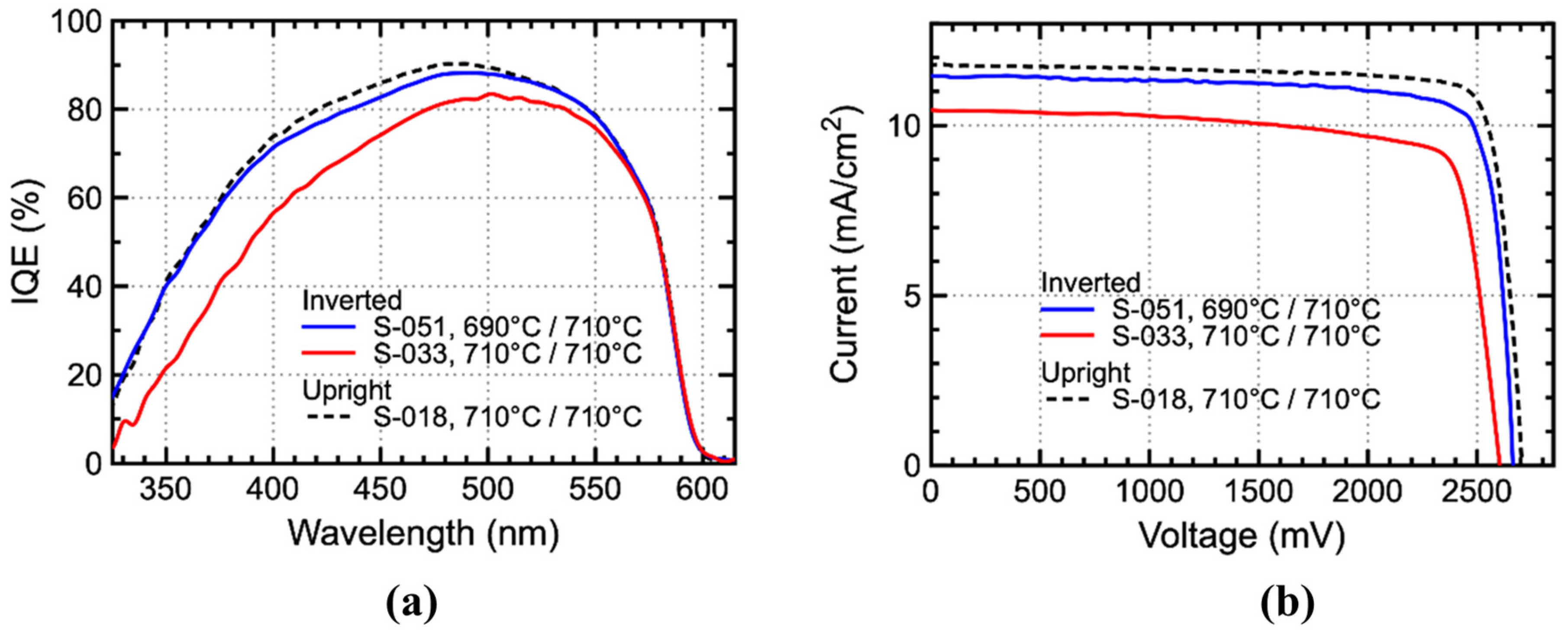
3.1.4. Fabrication of Improved Solar Cells

Based on the above results, an improved AlGaInP/AlGaAs inverted solar cell with a lower growth temperature of the Si-doped AlInP window layer is fabricated. As shown in Table 2 and Figure 4, the Si-doped AlInP window layer grown at 690 °C could achieve a high doping concentration without the deterioration of the material quality and result in tradeoffs between the IQE and FF.
Figure 6 shows the IQE and I-V curves of the improved inverted solar cell (S-051). As a contrast, the results of the conventional inverted cell (S-033) and upright cell (S-018) are also presented. All three solar cells have the same doping level in the emitter layers, which is 3 × 1018 cm−3. The doping level in the window layer of S-051 (6 × 1018 cm−3) is slightly lower than that of S-033 and S-018 (7 × 1018 cm−3). In Figure 6a, the peak IQE of the improved inverted AlGaInP solar cells rises from 83.3% to 88.2%. The IQE curve of the improved cell shows an almost full recovery from that of the upright cell except for a small gap in the 400 to 500 nm range. In addition, the Jsc of the optimized inverted AlGaInP cell rises from 10.45 mA/cm2 to 11.47 mA/cm2. The fill factor also improves from 0.789 to 0.827, resulting in an improvement in the IV curve shape. Optimized AlGaInP/AlGaAs dual-junction solar cells achieve a 60 mV Voc increment compared with the traditional structure, resulting in an enhanced efficiency from 15.87% to 18.68% for dual-junction AlGaInP/AlGaAs solar cells. As shown in Table 3, the performance of the improved cell (S-051) is still lower than the upright cell (S-018). The performance difference might be attributed to the thermal load of the AlGaInP sub-cell and tunnel junction [15,34,35,36], which is at the bottom of the dual-junction solar cell. Dopant diffusion in the active layer would cause Voc loss and have an impact on the p-n junction. However, the recovered IQE and Jsc values of S-051 clearly demonstrate the effect of the Si-doped AlInP window layer on the performance of the inverted AlGaInP solar cell.
Improved carrier collection efficiency of the AlGaInP sub-cell helps to enhance the current-match condition of the T-3J solar cell and improve the solar cell performance. The optimized inverted GaAs T-3J sub-cell is then applied to the fabrication of the SBT five-junction solar cell. The bottom two-junction solar cell (B-2J) consists of InGaAsP (1.04 eV) and InGaAsP (0.8 eV), which is deposited lattice-matched to the InP substrate and has been well-optimized [10,37]. The GaAs T-3J and InP B-2J sub-cell are then processed through the semiconductor direct bonding technique to form a two-terminal 5J solar cell. After the standard III-V-device-fabricated process, a broadband ZnS/MgF2 ARC is deposited on top of the surface to reduce current loss. Then, the fabricated 5J solar cell is measured under the AM0 spectrum simulator with multiple reference cell calibration. With the improvement in the AlGaInP top-cell, the SBT-5J solar cell achieves an efficiency of 35.39% (AM0, 25 °C) [10], which shows a Voc of 4.925 V, a Jsc of 11.37 mA/cm2 and an FF of 0.8554.

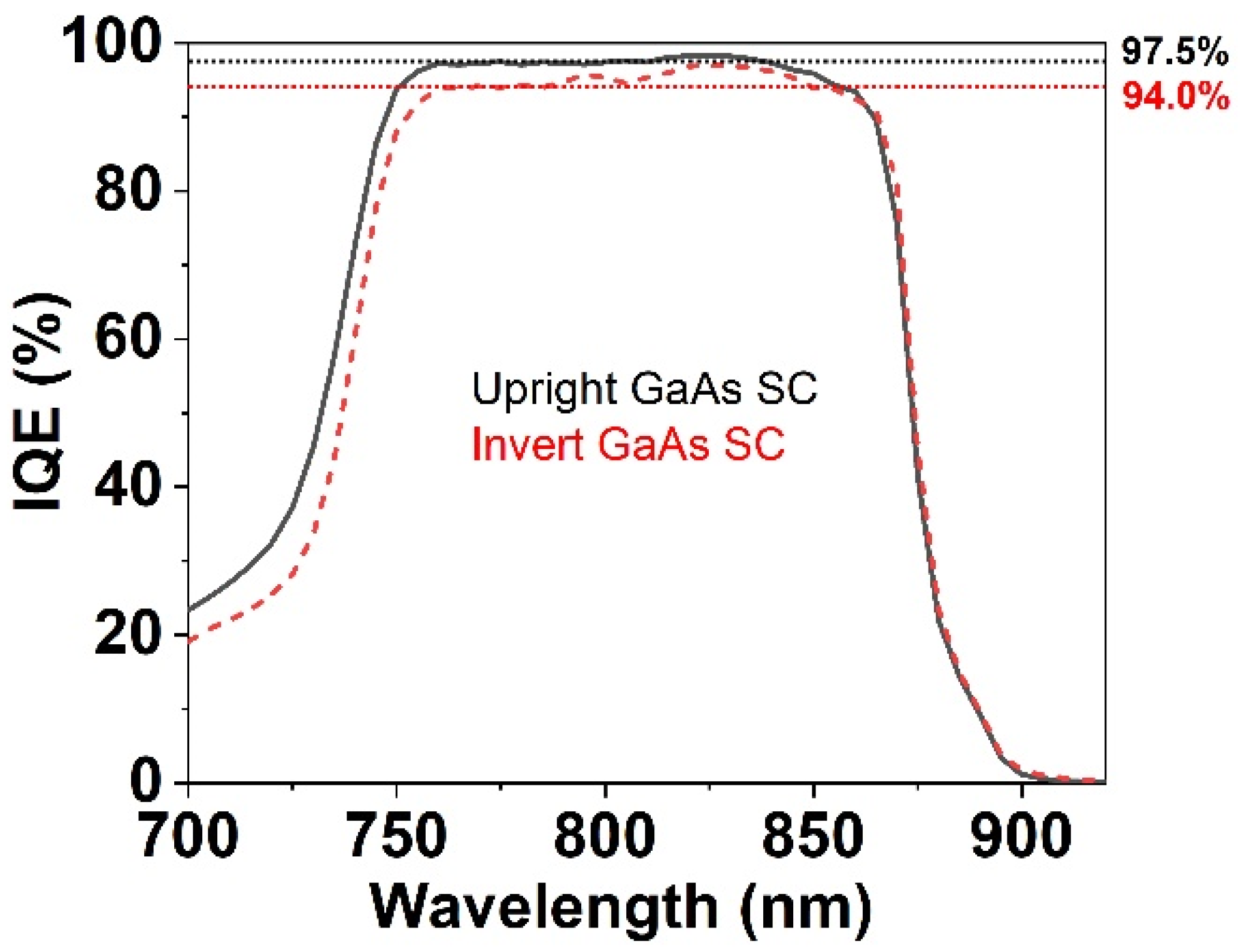
3.2. Structure Optimization in GaAs Sub-Cell

The SBT-5J solar cell performance has been increased through the optimization of the AlInP window layer in inverted AlGaInP sub-cells. However, as shown in Figure 2, inverted GaAs sub-cells also slightly suffer from poor material quality of the Si-doped AlInP window layer. For the upright GaAs solar cell structure, the AlInP window layer is deposited after the Si-doped GaAs emitter layer and Zn-doped GaAs base layer, acting as a passivation layer to prevent minority carrier transport from the emitter. On the contrary, inverted GaAs sub-cells will deposit the AlInP window layer first. As discussed earlier, the Si-doped AlInP window layer in inverted solar cells will deteriorate the subsequent active layer and decrease the solar cell performance. As shown in Figure 7, GaAs solar cells with an upright and inverted structure are fabricated and measured. Both GaAs solar cells have an AlGaAs absorbing layer to simulate the GaAs sub-cell in multi-junction solar cells. The structure and doping profile of both solar cells are identical, which all have a 3500 nm p-GaAs base layer, 100 nm n+-GaAs emitter layer and 120 nm n+-AlInP window layer. The IQE of the upright GaAs solar cell remains 97.5% between 750 nm and 850 nm. However, the IQE of the inverted GaAs solar cell decreases, especially in a short wavelength, between 750 nm and 800 nm. The IQE of the inverted GaAs solar cell suggests decreased carrier collection efficiency in the GaAs emitter layer, which is suggested to be caused by the Si-doped AlInP window layer beneath the GaAs emitter layer.
As shown in the optimization route of AlGaInP solar cells, the Si-doped AlInP window layer beneath the GaAs active layer would have impacts on the subsequent emitter layer. According to a calculated band diagram of the GaAs sub-cell [10], the interface recombination velocity between the GaAs emitter and AlInP window layer will also influence the carrier collection efficiency in a short wavelength, which would also cause recombination loss in the GaAs emitter layer. An optimization of the solar cell structure is performed to mitigate the effect that uses a wide bandgap emitter layer in the GaAs solar cell. GaAs heterojunction solar cells with a wide bandgap emitter will decrease the photon generation rate in the emitter layer near the GaAs band edge and, therefore, decrease the recombination rate in the emitter layer [38]. In multi-junction solar cells, the GaAs heterojunction sub-cell is more effective because the high-energy photon is mostly absorbed in the top sub-cell. Recombination loss in the wide bandgap emitter layer could be partly eliminated. Band discontinuities in the heterointerface will cause band offset between the base layer and wide bandgap emitter layer. A large band offset in the conduction band interface will suppress electron transport from the depletion region to the emitter and deteriorate solar cell performance [39]. It is important to minimize the band offset in a p-n heterojunction. AlInP, GaInP and AlGaAs are commonly used wide bandgap emitter layers with a p-GaAs base layer. Among them, the GaInP/p-GaAs heterojunction has minimized the band offset, which is 0.08 eV, and is most suitable for GaAs heterojunction solar cells [39,40,41,42].
With a set of optimization route, a 20 nm Si-doped GaInP emitter layer is introduced in the inverted GaAs sub-cell to mitigate the effect of the AlInP window layer. The doping level of the Si-doped GaInP emitter layer is 2 × 1018 cm−3. The GaAs sub-cell is grown at 680 °C to achieve a better performance. An inverted AlGaInP/AlGaAs/GaAs 3J solar cell is then fabricated. The inverted 3J solar cell is processed with semiconductor bonding technology with an InP buffer layer. With the help of decreased recombination loss and improved built-in potential [43,44], the optimized 3J solar cell achieves a Voc of 3830 mV and an FF of 0.854 under AM0 illumination. The IQE curves in Figure 8b show that the GaInP/p-GaAs heterojunction solar cell retains the same carrier collection efficiency with the GaAs homojunction solar cell. Unwanted low carrier collection efficiency in the wide bandgap GaInP emitter is avoided by the design of the multi-junction structure.
As the performance of the GaAs T-3J solar cell is improved by the GaAs sub-cell, previously fabricated 5J solar cells [10] could be enhanced further. SBT-5J solar cells with GaAs heterojunction sub-cells are fabricated using the standard III-V-device-fabricated process. The solar cell area is 2 × 2 cm2 in size. The bandgap of the 5J solar cell is 2.1 eV, 1.7 eV, 1.4 eV, 1.04 eV and 0.80 eV, respectively. The calculated current density of the sub-cell from the EQE curve is shown in Figure 9a. This agrees with the light IV measurement under the AM0 spectrum, which shows a Jsc of 11.29 mA/cm2. After the optimization of the AlGaInP and GaAs sub-cells, optimized 5J solar cells achieve an excellent performance. The solar cell efficiency improves to 35.61% under the AM0 spectrum (AM0, 25 °C). An enhanced Voc of 4961 mV and FF of 0.861 are achieved. The average voltage loss of the sub-cell could be estimated to be around 410 mV.

4. Conclusions

The effect of an Si-doped AlInP window layer on the performance of an SBT-5J solar cell was studied. It was confirmed that a higher growth temperature damages the quality of the Si-doped AlInP window layer, and it further deteriorates the subsequent active layers, which is supported by the results from the carrier lifetime investigation. Based on that, improved growth sequences for inverted 2.1 eV AlGaInP solar cells and improved n-GaInP/p-GaAs heterojunction structures for GaAs solar cells were then proposed. By the optimization of the inverted T-3J solar cell structure, the influence of the heavily Si-doped AlInP window layer is decreased. A fabricated inverted AlGaInP sub-cell achieves an enhanced QE of 10% to 20% and the peak IQE rises from 83.3% to 88.2%, which presents a nearly identical IQE compared with the upright reference. Further optimization in GaAs sub-cells decreases the recombination loss in the emitter caused by the poor AlInP window layer. The optimized structure significantly improves the Voc of inverted GaAs-based 3J solar cells to 3830 mV, boosting the efficiency of the five-junction solar cells to 35.61% under AM0 illumination. The demonstration confirms the important role of the Si-doped AlInP window layer during the growth of inverted solar cells.

Supplementary Materials

The following supporting information can be downloaded at: https://www.mdpi.com/article/10.3390/photonics9060404/s1.

Author Contributions

Conceptualization, G.L. and W.Z.; methodology, G.L. and H.L.; software, X.L.; validation, G.L., H.L. and X.L.; formal analysis, G.L.; investigation, G.L. and H.L.; resources, X.L.; data curation, G.L.; writing—original draft preparation, G.L.; writing—review and editing, W.Z.; visualization, G.L.; supervision, X.L.; project administration, W.Z.; funding acquisition, X.L. All authors have read and agreed to the published version of the manuscript.

Funding

This research was funded by National Natural Science Foundation of China (grant number 62104147 and 62004126).

Institutional Review Board Statement

Not applicable.

Informed Consent Statement

Not applicable.

Data Availability Statement

Not applicable.

Acknowledgments

The authors express their appreciation to the anonymous reviewers for their valuable suggestions.

Conflicts of Interest

The authors declare no conflict of interest.

References

  1. Geisz, J.F.; France, R.M.; Schulte, K.L.; Steiner, M.A.; Norman, A.G.; Guthrey, H.L.; Young, M.R.; Song, T.; Moriarty, T. Six-junction III–V solar cells with 47.1% conversion efficiency under 143 Suns concentration. Nat. Energy 2020, 5, 326–335. [Google Scholar] [CrossRef]
  2. Yamaguchi, M.; Takamoto, T.; Araki, K.; Ekins-Daukes, N. Multi-junction III–V solar cells: Current status and future potential. Sol. Energy 2005, 79, 78–85. [Google Scholar] [CrossRef]
  3. Green, M.; Dunlop, E.; Hohl-Ebinger, J.; Yoshita, M.; Kopidakis, N.; Hao, X. Solar cell efficiency tables (version 57). Prog. Photovolt. 2021, 29, 3–15. [Google Scholar] [CrossRef]
  4. Pakhanov, N.A.; Andreev, V.M.; Shvarts, M.Z.; Pchelyakov, O.P. State-of-the-art Architectures and Technologies of High-Efficiency Solar Cells Based on III–V Heterostructures for Space and Terrestrial Applications. Optoelectron. Instrum. Data Process. 2018, 54, 187–202. [Google Scholar] [CrossRef]
  5. Geisz, J.F.; Steiner, M.A.; Jain, N.; Schulte, K.L.; France, R.M.; McMahon, W.E.; Perl, E.E.; Friedman, D.J. Building a Six-Junction Inverted Metamorphic Concentrator Solar Cell. IEEE J. Photovolt. 2018, 8, 626–632. [Google Scholar] [CrossRef]
  6. Chiu, P.T.; Law, D.C.; Singer, S.B.; Bhusari, D.; Zakaria, A.; Liu, X.Q.; Mesropian, S.; Karam, N.H. High performance 5J and 6J direct bonded (SBT) space solar cells. In Proceedings of the 2015 IEEE 42nd Photovoltaic Specialist Conference (PVSC), New Orleans, LA, USA, 14–19 June 2015; pp. 1–3. [Google Scholar]
  7. Chiu, P.; Law, D.; Woo, R.; Singer, S.; Bhusari, D.; Hong, W.; Zakaria, A.; Boisvert, J.; Mesropian, S.; King, R. Direct semiconductor bonded 5J cell for space and terrestrial applications. IEEE J. Photovolt. 2014, 4, 493–497. [Google Scholar] [CrossRef]
  8. France, R.M.; Dimroth, F.; Grassman, T.J.; King, R.R. Metamorphic epitaxy for multijunction solar cells. MRS Bull. 2016, 41, 202–209. [Google Scholar] [CrossRef]
  9. Guter, W.; Schöne, J.; Philipps, S.P.; Steiner, M.; Siefer, G.; Wekkeli, A.; Welser, E.; Oliva, E.; Bett, A.W.; Dimroth, F. Current-matched triple-junction solar cell reaching 41.1% conversion efficiency under concentrated sunlight. Appl. Phys. Lett. 2009, 94, 223504. [Google Scholar] [CrossRef]
  10. Li, X.; Li, G.; Lu, H.; Zhang, W. >35% 5-junction space solar cells based on the direct bonding technique. J. Semicond. 2021, 42, 122701. [Google Scholar] [CrossRef]
  11. Li, X.; Zhang, W.; Zhang, J.; Lu, H.; Zhou, D.; Sun, L.; Chen, K. Study on 2.05 eV Al0.13GaInP sub-cell and its hetero-structure cells. In Proceedings of the 2014 IEEE 40th Photovoltaic Specialist Conference (PVSC), Denver, CO, USA, 8–13 June 2014; pp. 479–481. [Google Scholar]
  12. Sun, Y.; Fan, S.; Faucher, J.; Hool, R.D.; Li, B.D.; Dhingra, P.; Lee, M.L. 2.0–2.2 eV AlGaInP solar cells grown by molecular beam epitaxy. Sol. Energy Mater. Sol. Cells 2021, 219, 110774. [Google Scholar] [CrossRef]
  13. Perl, E.E.; Simon, J.; Geisz, J.F.; Olavarria, W.; Young, M.; Duda, A.; Friedman, D.J.; Steiner, M.A. Development of high-bandgap AlGaInP solar cells grown by organometallic vapor-phase epitaxy. IEEE J. Photovolt. 2016, 6, 770–776. [Google Scholar] [CrossRef]
  14. Steiner, M.A.; France, R.M.; Perl, E.E.; Friedman, D.J.; Simon, J.; Geisz, J.F. Reverse Heterojunction (Al)GaInP Solar Cells for Improved Efficiency at Concentration. IEEE J. Photovolt. 2020, 10, 487–494. [Google Scholar] [CrossRef]
  15. Hinojosa, M.; García, I.; Rey-Stolle, I.; Algora, C. Evidence of enhanced Zn-diffusion observed during the growth of Inverted Metamorphic Solar Cells. In Proceedings of the 2019 IEEE 46th Photovoltaic Specialists Conference (PVSC), Chicago, IL, USA, 16–21 June 2019; pp. 49–53. [Google Scholar]
  16. Steiner, M.A.; Geisz, J.F.; Reedy, R.C.; Kurtz, S. A direct comparison of inverted and non-inverted growths of GaInP solar cells. In Proceedings of the 2008 33rd IEEE Photovoltaic Specialists Conference, San Diego, CA, USA, 11–16 May 2008; pp. 1–6. [Google Scholar]
  17. Li, X.; Zhang, W.; Lu, H.; Chen, K.; Zhou, D. Growth of tellurium doped ultra-broadband tunnel junction for the next generation 5J solar cell. J. Cryst. Growth 2014, 405, 16–18. [Google Scholar] [CrossRef]
  18. Dimroth, F.; Grave, M.; Beutel, P.; Fiedeler, U.; Karcher, C.; Tibbits, T.N.; Oliva, E.; Siefer, G.; Schachtner, M.; Wekkeli, A. Wafer bonded four-junction GaInP/GaAs//GaInAsP/GaInAs concentrator solar cells with 44.7% efficiency. Prog. Photovolt. 2014, 22, 277–282. [Google Scholar] [CrossRef]
  19. Zhang, M.; Ning, T.; Chen, J.; Sun, L.; Zhou, L. Improvement on the interface properties of p-GaAs/n-InP heterojunction for wafer bonded four-junction solar cells. J. Mater. Sci. Technol. 2019, 35, 330–333. [Google Scholar] [CrossRef]
  20. Cederberg, J.; Bieg, B.; Huang, J.-W.; Stockman, S.; Peanasky, M.; Kuech, T. Intrinsic and oxygen-related deep level defects in In0.5 (AlxGa1−x)0.5P grown by metal-organic vapor phase epitaxy. J. Cryst. Growth 1998, 195, 63–68. [Google Scholar] [CrossRef]
  21. Tukiainen, A.; Dekker, J.; Leinonen, T.; Pessa, M. Characterization of deep levels in rapid-thermal-annealed AlGaInP. Mater. Sci. Eng. B 2002, 91, 389–392. [Google Scholar] [CrossRef]
  22. Kondo, M.; Okada, N.; Domen, K.; Sugiura, K.; Anayama, C.; Tanahashi, T. Origin of nonradiative recombination centers in AlGaInP grown by metalorganic vapor phase epitaxy. J. Electron. Mater. 1994, 23, 355–358. [Google Scholar] [CrossRef]
  23. Lee, K.-J.; Chen, H.; Chen, J. Photoluminescence of the Se and Si DX centers in (AlxGa1−x)0.5In0.5P (x < 0.5) grown by metalorganic vapor phase epitaxy. J. Appl. Phys. 1997, 82, 1350–1354. [Google Scholar] [CrossRef]
  24. Nojima, S.; Tanaka, H.; Asahi, H. Deep electron trapping center in Si-doped InGaAlP grown by molecular-beam epitaxy. J. Appl. Phys. 1986, 59, 3489–3494. [Google Scholar] [CrossRef]
  25. Huang, Z.; Wie, C.; Varriano, J.; Koch, M.; Wicks, G. Phosphorus-vacancy-related deep levels in GaInP layers. J. Appl. Phys. 1995, 77, 1587–1590. [Google Scholar] [CrossRef]
  26. Kosa, A.; Stuchlikova, L.; Harmatha, L.; Mikolasek, M.; Kovac, J.; Sciana, B.; Dawidowski, W.; Radziewicz, D.; Tlaczala, M. Defect distribution in InGaAsN/GaAs multilayer solar cells. Sol. Energy 2016, 132, 587–590. [Google Scholar] [CrossRef]
  27. Zhang, X.; Hu, J.; Wu, Y.; Lu, F. Direct observation of defects in triple-junction solar cell by optical deep-level transient spectroscopy. J. Phys. D Appl. Phys. 2009, 42, 145401. [Google Scholar] [CrossRef]
  28. Leon, C.; Le Gall, S.; Gueunier-Farret, M.-E.; Kleider, J.-P. How to perform admittance spectroscopy and DLTS in multijunction solar cells. Sol. Energy Mater. Sol. Cells 2022, 240, 111699. [Google Scholar] [CrossRef]
  29. Dobaczewski, L.; Kaczor, P.; Żytkiewicz, Z.R.; Missous, M.; Saleemi, F.; Dawson, P.; Peaker, A.R. Hole capture at the DX(Si) and DX(Te) defects in AlxGa1−xAs. J. Appl. Phys. 1992, 72, 3198–3200. [Google Scholar] [CrossRef]
  30. Stockman, S.; Huang, J.-W.; Osentowski, T.; Chui, H.; Peanasky, M.; Maranowski, S.; Grillot, P.; Moll, A.; Chen, C.; Kuo, C. Oxygen incorporation in AllnP, and its effect on P-type doping with magnesium. J. Electron. Mater. 1999, 28, 916–925. [Google Scholar] [CrossRef]
  31. Hovel, H.J. Semiconductors and Semimetals. Volume 11. Solar Cells; Academic Press, Inc.: New York, NY, USA, 1975. [Google Scholar]
  32. Yu, Q.; Raiwu, P.; Cuiyun, L. Effect of VIII ratio on the electrical and optical properties of Si-doped AlGaInP grown by metalorganic chemical vapor deposition. J. Cryst. Growth 1995, 148, 13–16. [Google Scholar] [CrossRef]
  33. Nelson, J. The Physics of Solar Cells; World Scientific Publishing Company: Singapore, 2003. [Google Scholar]
  34. García, I.; Ochoa, M.; Lombardero, I.; Cifuentes, L.; Hinojosa, M.; Caño, P.; Rey-Stolle, I.; Algora, C.; Johnson, A.; Davies, I.; et al. Degradation of subcells and tunnel junctions during growth of GaInP/Ga(In)As/GaNAsSb/Ge 4-junction solar cells. Prog. Photovolt. 2017, 25, 887–895. [Google Scholar] [CrossRef] [Green Version]
  35. Rey-Stolle, I.; García, I.; Barrigón, E.; Olea, J.; Pastor, D.; Ochoa, M.; Barrutia, L.; Algora, C.; Walukiewicz, W. On the thermal degradation of tunnel diodes in multijunction solar cells. AIP Conf. Proc. 2017, 1881, 040005. [Google Scholar] [CrossRef] [Green Version]
  36. Dawidowski, W.; Ściana, B.; Zborowska-Lindert, I.; Mikolášek, M.; Kováč, J.; Tłaczała, M. Tunnel junction limited performance of InGaAsN/GaAs tandem solar cell. Sol. Energy 2021, 214, 632–641. [Google Scholar] [CrossRef]
  37. Lu, H.; Li, X.; Zhang, W.; Li, G.; Hu, S.; Dai, N. MOVPE grown 1.0 eV InGaAsP solar cells with bandgap-voltage offset near to ideal radiative recombination limit. Sol. Energy Mater. Sol. Cells 2019, 196, 65–69. [Google Scholar] [CrossRef]
  38. Gudovskikh, A.; Zelentsov, K.; Kalyuzhnyy, N.; Lantratov, V.; Mintairov, S. Anisotype GaAs based heterojunctions for III-V multijunction solar cells. In Proceedings of the 25th European Photovoltaic Solar Energy Conference, Valencia, Spain, 6–10 September 2010; pp. 472–476. [Google Scholar]
  39. Hwang, S.-T.; Kim, S.; Cheun, H.; Lee, H.; Lee, B.; Hwang, T.; Lee, S.; Yoon, W.; Lee, H.-M.; Park, B. Bandgap grading and Al0.3Ga0.7As heterojunction emitter for highly efficient GaAs-based solar cells. Sol. Energy Mater. Sol. Cells 2016, 155, 264–272. [Google Scholar] [CrossRef]
  40. Adachi, S. GaAs, AlAs, and Al × Ga1 − xAs: Material parameters for use in research and device applications. J. Appl. Phys. 1985, 58, R1–R29. [Google Scholar] [CrossRef]
  41. Bour, D.; Shealy, J.; Wicks, G.; Schaff, W. Optical properties of Alx In1−xP grown by organometallic vapor phase epitaxy. Appl. Phys. Lett. 1987, 50, 615–617. [Google Scholar] [CrossRef]
  42. Vurgaftman, I.; Meyer, J.R.; Ram-Mohan, L.R. Band parameters for III–V compound semiconductors and their alloys. J. Appl. Phys. 2001, 89, 5815–5875. [Google Scholar] [CrossRef] [Green Version]
  43. Ragay, F.; Ruigrok, E.; Wolter, J. GaAs-AlGaAs heterojunction solar cells with increased open-circuit voltage. In Proceedings of the 1994 IEEE 1st World Conference on Photovoltaic Energy Conversion-WCPEC (A Joint Conference of PVSC, PVSEC and PSEC), Waikoloa, HI, USA, 5–9 December 1994; pp. 1934–1937. [Google Scholar]
  44. Jensen, N.; Rau, U.; Hausner, R.; Uppal, S.; Oberbeck, L.; Bergmann, R.; Werner, J. Recombination mechanisms in amorphous silicon/crystalline silicon heterojunction solar cells. J. Appl. Phys. 2000, 87, 2639–2645. [Google Scholar] [CrossRef]
Figure 1. Schematic cross-section structure of inverted GaAs T-3J sub-cell.
Photonics 09 00404 g001
Figure 2. IQE spectra of fabricated AlGaInP/AlGaAs/GaAs (2.1 eV/1.7 eV/1.4 eV) T-3J solar cells grown in upright (solid line) and inverted structure (dashed line). Inverted 2.1 eV AlGaInP sub-cell presents decreased IQE compared with upright reference.
Photonics 09 00404 g002
Figure 3. IQE curves of inverted 2.1 eV AlGaInP sub-cells grown at different temperatures (690 °C–720 °C, solid line), showing that higher temperature reduces carrier collection efficiency. Upright 2.1 eV AlGaInP sub-cell grown at 710 °C is set as benchmark (dashed line).
Photonics 09 00404 g003
Figure 4. IQE curves of inverted 2.1 eV AlGaInP solar cells grown at 710 °C (S-033, S-039 and S-040) and 690 °C (S-043) with varied doping concentrations in emitter and window layer (detailed doping levels of samples are listed in Table 2). Reduced Si doping level in emitter has little effect on IQE, while reduced Si doping level in window causes an IQE recovery. In addition, Si-doped AlInP window layer grown at lower temperature results in better material quality and enhanced IQE.
Photonics 09 00404 g004
Figure 5. PL decays of AlInP/AlGaInP double heterojunctions grown at varied temperature. The excitation and emission wavelength are 532 nm and 584.3 nm, respectively. The data are fitted using mono-exponential fitting.
Photonics 09 00404 g005
Figure 6. IQE curves (a) and light J–V curves (b) of inverted AlGaInP/AlGaAs (2.1 eV/1.7 eV) dual-junction solar cells before (red solid line) and after (blue solid line) optimization of window layer. The growth temperature is listed in Table 3. Upright AlGaInP solar cell sample grown at 710 °C (S-018) is set as benchmark (black dashed line).
Photonics 09 00404 g006
Figure 7. IQE spectra of fabricated GaAs solar cells grown in upright structure (black solid line) and inverted structure (red dashed line). Both GaAs solar cells have AlGaAs absorbing layer to simulate the GaAs sub-cell in multi-junction solar cells. Inverted GaAs solar cell presents decreased IQE compared with upright reference.
Photonics 09 00404 g007
Figure 8. Light J–V curves (a) and IQE curves (b) of inverted T-3J solar cell with varied GaAs sub-cell structures. GaAs sub-cell with GaAs/GaInP heterojunction structure (solid line) shows better performance than that with GaAs homojunction structure (dashed line).
Photonics 09 00404 g008
Figure 9. EQE curve (a) and light J–V curve (b) of SBT 5-junction solar cell. The bandgap combination of optimized SBT-5J solar cell is 2.1 eV, 1.7 eV, 1.4 eV, 1.04 eV and 0.8 eV, which is made of AlGaInP, AlGaAs, GaAs, InGaAsP and InGaAsP sub-cell, respectively. Light J–V curve is measured under AM0 spectrum (AM0, 25 °C) and calibrated by multiple reference cells.
Photonics 09 00404 g009
Table 1. Light J–V results of dual-junction solar cells (S-018, S-043, S-036, S-033 and S-037).
No.Temp. (°C)Jsc (mA)Voc (mV)Ff
S-01871011.7927050.850
S-04369011.2526560.732
S-03670011.1826070.813
S-03371010.4526040.791
S-0377209.3625750.809
Table 2. Light J–V results of dual-junction solar cells (S-033, S-039, S-040 and S-043).
No.Temp. (°C)Doping Level (cm−3)Jsc
(mA)
Voc
(mV)
Ff
EmitterWindow
S-0337103E187E1810.4526040.791
S-0397103E177E1810.3825400.758
S-0407103E177E1711.0725450.671
S-0436903E186E1811.2526560.732
Table 3. Light J–V results of dual-junction solar cells (S-033, S-051 and S-018).
No. Temp. (°C)Jsc
(mA)
Voc
(mV)
FfEff.
(%)
Win/Emitter
S-033inverted710/71010.4526040.78915.87
S-051inverted690/71011.4726640.82718.68
S-018upright710/71011.7927050.85020.03
Publisher’s Note: MDPI stays neutral with regard to jurisdictional claims in published maps and institutional affiliations.

