1. Introduction
Over the last few decades, the exponentially increasing demand for transmission capacity in optical fiber communication networks has led to the fast development of photonic integrated circuits (PICs) as an attractive and practical solution to expand capacity while keeping the cost low, compared to conventional solutions using the bulky assembly of discrete, free-space components [
1,
2]. Extra and often expensive procedures are needed to improve the stability and robustness of the free-space optical assembly to secure their applications in the daedal environment. The integration of optical components and functions into a large-scale PIC has shown clear advantages, as this technology keeps bringing new functionalities under reasonable power consumption and small footprint.
Beyond optical communication, PICs are expected to open up new ways to quench the ever-increasing thirst for computation power, raised by today’s big data and artificial intelligence technology [
3,
4]. The key advantage is that photonic computation is carried out by light propagation that needs essentially no processing power and allows parallel treatment of massive data. It would enable applications that are unreachable by conventional electronic computing technology, those requiring low latency, high bandwidth, and low power-consumption, at the same time [
5,
6].
Under PIC-based photonic computation technology, it is believed by many that the property of photons makes it difficult to realize optical digital gates, whereas in the electronic domain the logic gates can be readily made by a series of transistors. Nevertheless, optical logic gates have been reported with different waveguide structures, such as active Mach-Zehnder interferometers (MZIs) [
7,
8], microring resonators (MRRs) [
9], directional couplers (DCs) [
10], multimode interference devices (MMIs) [
11,
12], QR code-like nanostructures [
13], etc. Several material platforms, including silicon-on-insulator (SOI) [
9], plasmas [
14], lithium niobate [
15], photonic crystals [
16], nonlinear materials [
17], etc., are dedicated to implementing the on-chip logic operation for signal process and photonic computing. Two methods are widely used in PIC-based logic devices [
18]. The first method is based on the linear interference, where the input stays in the optical domain and the phases/amplitudes are taken to be the input logic states. This method is simple, convenient, and easy to implement with clear mechanics. However, it is still challenging to precisely control the phase difference between the various signals, though phase-shifted-keying [
11] has matured over the years and been implemented in practical transmission networks. As the devices often require high structure/phase accuracy in the fabrication process, many designs have not been verified experimentally [
10,
11,
12,
13,
14,
15,
17]. Furthermore, Ref. [
19] adopts the input logic as the electrical pulse train (EPS), instead of the optical phase. The continuous wave (CW) light signal is used as the carrier only. Although this method avoids the accurate control of optical phases, the input EPS needs modulate the microring resonators precisely and the output information is read out at specific resonant wavelengths, thus requiring a complex and expensive system with broadband tunable laser and spectrum analyzing equipment.
The cascaded methods can effectively extend the number of operation logic bits for a large-scale computing network. However, they suffer from the often inefficient optical-electrical-optical (O/E/O) conversions [
8]. The nonlinear optical effects can also be adopted to develop various kinds of complex logic devices. However, the nonlinear optical materials with large nonlinear susceptibility and ultrafast response are often expensive and require delicate processing.
In our previous works [
20,
21], we have demonstrated that the thermo-optic multimode waveguide is a powerful platform for programmable multi-functional PICs. The multimode interference (MMI) devices have shown desirable features, such as simple and compact structure, large bandwidth, low-loss, and good fabrication tolerance. The logic input can take the binary current values through the electrodes, while the input light can be continuous and works only as a carrier. Through a combination of thermo-optic and multimode interference effect, the output is converted into light intensity variations as defined in the truth table. However, the nonmonotonic response of the received light intensity with respect to the applied current makes it difficult to accurately predict the desirable logic functions. A current sweeping method can be introduced to search for the right configurations on the input and weight electrodes.
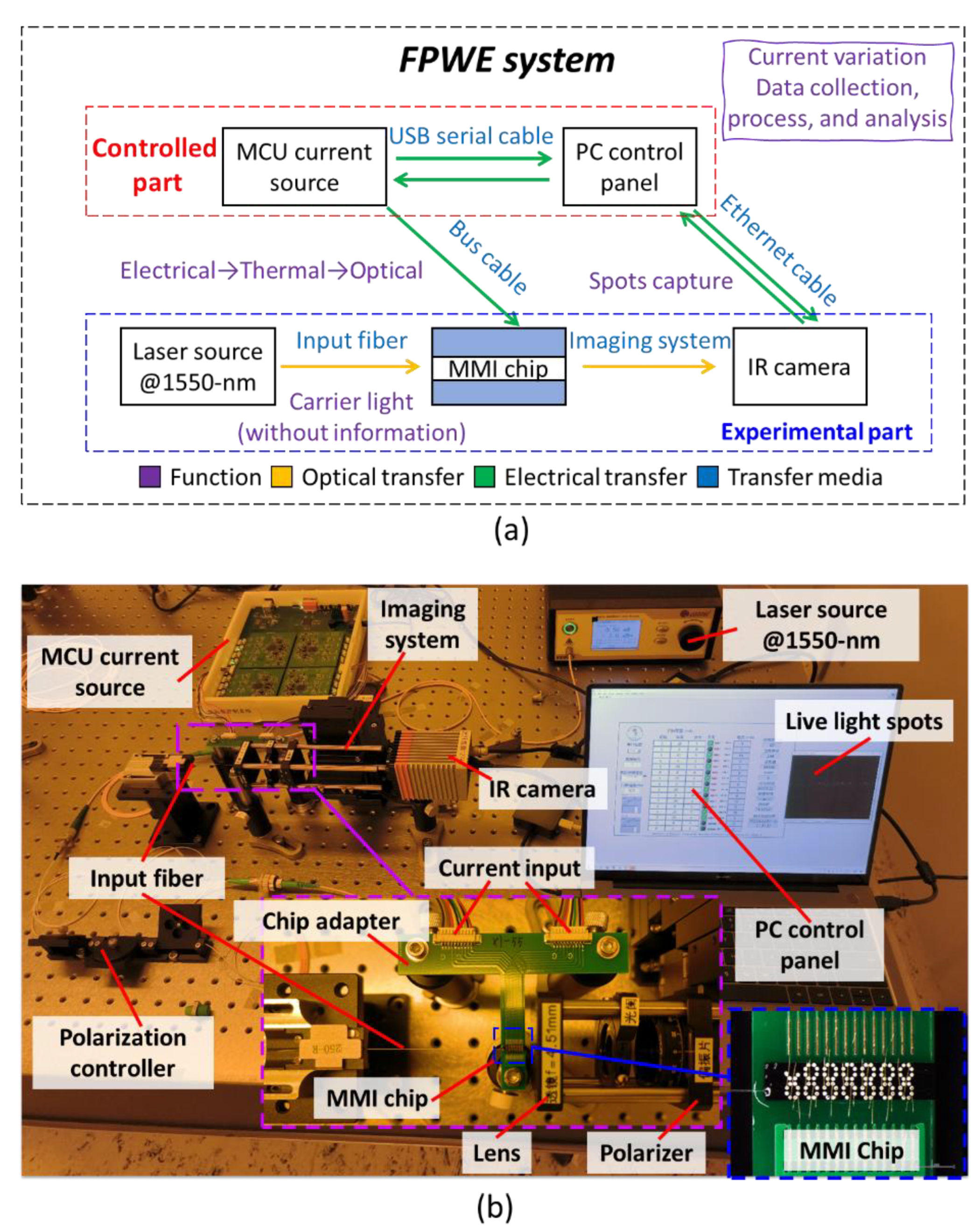
Recently, we have developed an optical computing/switching engine based on a multimode waveguide and a series of thermal electrodes to alter the light interference in the multimode region experimentally, actively, and automatically, until the desired pattern is reached at the output plane, so as to define the target function [
21]. We name it function programmable waveguide engine (FPWE). With this technology, an optical NOT logic gate is demonstrated, capable of processing 4 bits of electronic logic signals in parallel. In this work, we explore further into the FPWE technology and present a function versatile logic gate capable of parallel two-bit operation for the logic AND or OR function, defined by refreshing/updating the electrode (input and weight) settings. Going further on from the previous work [
21], the mechanism is investigated in detail, the data sorting algorithm is explained, and different levels of operations are explored for the target functions. We show that the proposed waveguide engine can even multiplex the logic AND and OR operations in parallel on the same chip with identical input, weight, and output. Only the bar values are set to be different for distinguishing the state of “0” and “1” for various logic operations.
In particular, we stress that the index tuning in the multimode region is a powerful method, as it can alter the total number of the guided eigenmodes, their individual modal profiles, as well as their propagation constants; while, in a single mode waveguide, the index tuning usually only varies the propagation constant, i.e., the phase of light passing through. We reveal that the thermal tuning process, similar to other E/O or O/E conversions, is essentially nonlinear, by drawing the curve relating the change of light intensity at a given output port to the electronic input in the form of current. This is fundamentally different to a conventional Mach-Zehnder interferometer (MZI) network, where the relation between the all-optical signals through the layers is considered as a linear transformation. This feature forms the foundation for the further development of the FPWE technology as an all-optical neutral network with built-in nonlinear activation function, but using only linear optical materials. This engine can be easily expanded, without cascades, to form a large-scale general hardware platform for the multi-bit logic operations and other versatile functions. We believe this work can inspire the development of programmable PICs for advanced communication and computing applications.
2. Engine Architecture and Working Mechanism
Figure 1a shows the architecture of the FPWE to be used as a logic gate. The input signal
A and
B, each containing two electrodes, i.e., two bits of logic information, are a subset of the electrode matrix
E. The input logic signals stay in the electronic domain and take the form of current through the electrode, i.e., low current for logic “0” and high current for logic “1”. The carrier light itself contains no information and the logic output
C is evaluated from the optical intensities measured on a subset of the waveguide outputs
O, as the result of the multimode interference.
The choice of electrodes forming
A [
Ea1, a2,
Ea3, a4] and
B [
Eb1, b2,
Eb3, b4] can be arbitrary based on the target functions.
Figure 1a shows only one possible option for
A and
B, but the input electrodes are not necessarily chosen next to each other.
A and
B must be independent, i.e., “
A∩
B = ∅”. The rest of the electrodes in
E are left as the weight matrix
W. The current flowing through the weight electrodes can be adjusted in multiple levels, or in an analog manner, in order to search for the ideal settings that satisfy the target truth table for the logic AND or OR operation.
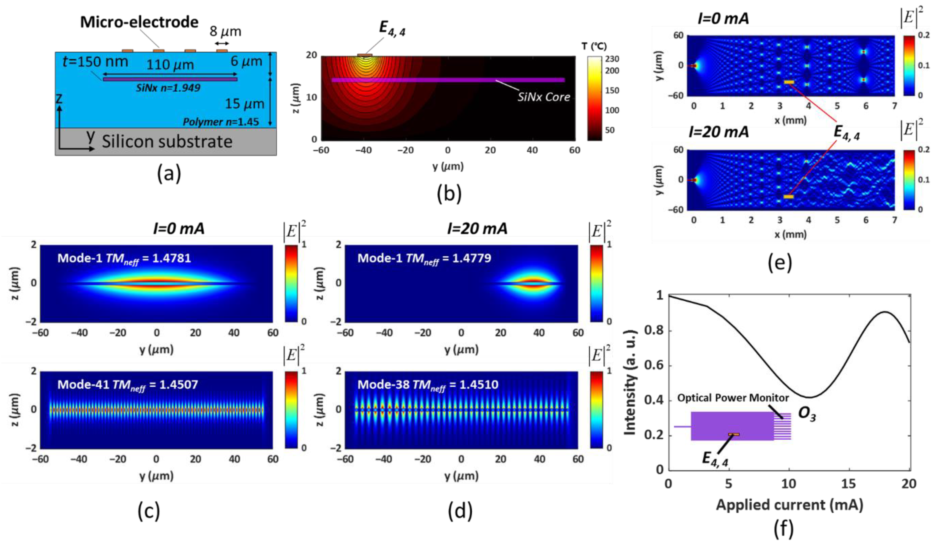
The actual chip design is displayed in
Figure 1b. The size of the MMI is designed as 7 mm × 110 μm. The input and output waveguides are placed symmetrically to the MMI waveguide. It contains 11 input waveguides on the left side and any waveguide can be chosen as the carrier light injection port. All the input waveguides go through a taper structure to improve the coupling with multimode waveguide. The gaps between the input tapers are set to 4 μm. Two out of 11 output waveguides can be chosen as the optical output
C. Output tapers are also added with a gap of 28 μm. A network of 4 × 7 thermal electrodes are placed on the multimode waveguide, each containing two pads (150 μm × 150 μm) for contact/bonding. The electrodes are labeled according to the row and column number. The gaps between each electrode column are set to be 1.0 mm along the propagation direction
x. In each column, the 4 electrodes are designed with the size of 150 μm × 8 μm. The redundancy in the waveguide ports as well as in the electrode number leaves room for the development of different logic and switching devices using the same chip, but under different input/weight/output choices.
The cross-section of the multimode waveguide is shown in
Figure 2a. We choose to work on silicon nitride (SiNx) waveguide in polymer for its relatively compact size, simple fabrication steps, high thermo-optic effect, and low thermal conductivity, as well as the intrinsic high waveguide birefringence that is essential for the development of polarization diversity devices, such as polarization-sensitive Bragg grating filters [
22], polarization beam splitter [
23], polarization rotator [
24], etc. The thickness of SiNx layer is 150 nm and the refractive index is 1.949 at 1550 nm, measured by an ellipsometer. The single-mode input/output waveguides have a width of 2 μm, while the width of the multimode waveguide is 110 μm. The polymer cladding (ZPU12 series from ChemOptics, Daejeon, Korea) has an index of 1.45. The top and bottom cladding thickness is 6 μm and 15 μm, respectively. The design concept can well be applied to other material platforms (e.g., silicon photonics, InP, silica PLC, polymer waveguide, etc.) and the refractive index tuning methods can also vary (thermo-optic effect, electro-optic effect, charge carrier injection, etc.).
Thermal electrodes of 150 μm in length, 8 μm in width, and 100-nm in thickness (10 nm Ti and 90 nm Au) are placed symmetrically on the surface of the top cladding with respect to the SiNx core. A 2D thermal solver (LUMERICAL HEAT) is used to calculate the temperature gradient numerically, assuming the silicon substrate as a heatsink (25 °C). The local cross-sectional temperature distribution when 20 mA current goes through one of the electrodes (
E4,4) is shown in
Figure 2b. The temperature distribution is translated to the change of the refractive index by the thermo-optic coefficient of the polymer cladding (−1.14 × 10
−4/°C) and the silicon nitride core (2.45 × 10
−5/°C). When a small heater power is applied, the index change is small, the gradient is smooth, and the extra scattering loss introduced by the electrodes can be neglected. However, the changed multimode interference under weakly applied heater power can still result in large power variations at the output waveguides, which constitute the logic-switching mechanism. In this work, we consider the TM modes only. As most of the light field for the guided modes resides in the cladding, the negative thermo-optic effect of the polymer material dominates [
25]. The eigenmode profiles are calculated using the mode solver from LUMERICAL MODE.
For the unheated waveguide shown in
Figure 2a, the structure supports 41 modes for the TM polarization, whereas for the heated condition shown in
Figure 2b, the structure supports only 38 modes with much altered profiles. The results are compared in
Figure 2c,d for the fundamental modes and the highest-order guided modes.
Figure 2e further compares the total light field in the XY plane for the unheated and heated cases, respectively, calculated using the bi-directional eigenmode expansion method. When an electrode is switched on, the change in the interference pattern is clearly visible. To quantify this change, a monitor is placed at the output waveguide
O3 to record the optical power passing through when a different current is applied to the electrode
E4,4, as an example. The curve is plotted in
Figure 2f, demonstrating a nonmonotonic and nonlinear change of the optical power change in response to the electronic current applied.
As it is difficult to conclude the response of the MMI waveguide by an analytical formula for any local refractive index change, the following empirical design rules are suggested when constructing a MMI-based logic gate. Firstly, the chosen multimode waveguide should support sufficient eigenmodes. The rule of thumb is to include at least 2 N modes, with N being the required output number. Once the waveguide thickness is set by the technology, the width can be varied to set the limit for higher order modes. Next, the multimode waveguide should be sufficiently long, so that the untuned MMI can at least reach the first 1 × N imaging point. However, the waveguide should not be much longer after the first 1 × 1 self-imaging point, as the MMI is intrinsically periodic. Extra length may facilitate interference tuning but would also result in an inefficient device. Finally, at least two columns of electrodes should be included, one column as the input and the other as weights. More weight electrodes would indeed allow for more complicated tuning of the MMI effect, but would also complicate the search process. One can leave some of the electrodes redundant, and only activate them if the search process fails.
The curve in
Figure 2f comes as no surprise. From Ohm’s law, the steady thermal power
Q is related to the current by
Q =
I2R, where
R is the resistance of the electrode, and
I is the applied current. At steady state, the thermal power is related to the temperature change by the heat transport equation:
where
k is the thermal conductivity, ∇
T is the temperature gradient,
V is the volume, and
J is the current density.
The heat transport equation can be solved numerically. The induced refractive index change Δ
n is related to the temperature change Δ
T (before heating and upon heating at a steady state) by:
where
ct is the thermo-optic coefficient (−1.14 × 10
−4/°C) of the material and can be regarded as a constant within a reasonable temperature range. Under a given refractive index distribution, the eigenmodes can then be solved by Maxwell’s equations. The total optical field at the output
Etot of a MMI waveguide can be given by:
where
x is the propagation direction and
y,
z is the profile which is perpendicular to the x direction.
ϕv(
y,
z) is the eigenmode field, and
βv is their respective propagation constant.
cv is the coupling coefficient of the individual eigenmode numbered by
v to the input light field, and
m is the total number of the guided modes supported by the multimode waveguide [
26]. The detected power
Po at one of the output ports
xo is proportional to the integral of the total intensity over the waveguide region:
Through this chain of electrical–thermal–optical changes, one can expect a complicated, nonmonotonic function of
Po with respect to the applied current signal
I. This function can be calculated numerically once the structure and material parameters are determined. The obtained curve in
Figure 2f can also be fitted using a combination of analytical functions for a given current range. The significance is that it enables a nonlinear response of the output to the input when the input signals stay in the electronic domain and the output signals are taken as the corresponding light amplitude/intensity changes in the optical domain. We therefore expect that complex functions can be realized without resorting to nonlinear optical materials or other O/E/O conversions, e.g., in constructing deep neural networks for data sorting and image classification. In this work, however, we confine it to the function of logic gates only and leave AI-based applications for future development.
4. Data Acquisition, Analysis, and Discussion
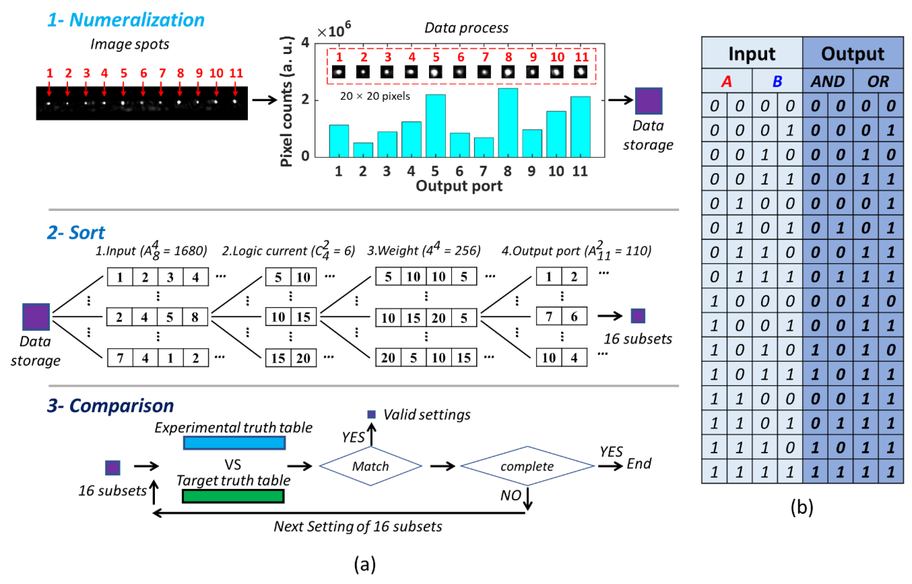
To collect the data, we have developed a program to scan the electrode current values and store the camera shots automatically. We do not distinguish the input and weight electrodes at the data acquisition stage. At first, 8 electrodes [E2,1 (22.0 Ω), E1,2 (21.1 Ω), E2,3 (22.6 Ω), E1,4 (20.4 Ω), E2,5 (21.3 Ω), E1,6 (19.8 Ω), E2,7 (21.1 Ω), E4,7 (21.3 Ω)] are chosen, and the current can take 4 values [5 mA, 10 mA, 15 mA, 20 mA]. The total thermal power consumption ranges from 4.2 mW (5 mA is applied to all the 8 electrodes) to 67.8 mW (20 mA is applied to all the 8 electrodes). The rest of the electrodes remain off. In total, these combinations constitute 48 = 65,536 experiments, each resulting in an image of 523 kilobytes (PNG format, 640 × 512 pixels, 16-bit resolution). The scan process is complete within 9.1 h (0.5 s for each sweeping), storing around 32.6 gigabytes of data on the hard drive. After data collection, a program is developed to search for the target logic operations.
Among these data, 4 out of 8 electrodes need to be chosen as input A and B, as each input contains two bits, totaling A84 = 1680 variations. It is noted that the sorting uses “permutation” rather than “combination”, because the order between A (the first operation bits) and B (the second operation bits) and their respective high and low bits should all be distinguished as different configurations. For example, A = [E2,1, E1,2]/B = [E2,3, E1,4] and A = [E2,3, E1,4]/B = [E2,1, E1,2] are different configurations, though they use the same 4 electrodes. Two of the 4 applied current values need to denote the logic “0” (relatively low current) and “1” (relatively high current) state for all the logic bits in A and B (C42 = 6). The other 4 electrodes remain as weights, which are fixed during the defined logic operations. Each of the weights can have one of the 4 current values, and the total number of the weight setting is calculated to be 44 = 256 for each specific input electrodes configuration. Two out of 11 waveguides should be chosen as the output C, adding up to A112 = 110 options. Here, it also uses “permutation”, not “combination”, because the output values must be distinguished with high and low bits.
The sorting program must therefore process 1680 × 6 × 256 × 110 = 283,852,800 possible configurations. We name each combination as one setting. For each setting, the program must try 24 = 16 variations of the input states to compare with the target truth table for either logic AND or OR operation. A MATLAB program is developed to test the settings in parallel. Although the parallel computing toolbox of MATLAB is powerful, it is still time-consuming and may run out of memory if all 283,852,800 configurations are searched together. Therefore, we divided the data into 2 parts in the following search process. The first part is based on the input electrodes and their binary current values (1680 × 6). After that, the remaining configurations of the weights and their output ports (256 × 110) are individually implemented for each preprocessed configuration. If all the 16 input variations and their outputs satisfy the truth table, this setting, i.e., the specific combination of electrode selection, current choice, and waveguide outport selection, is recorded as a valid setting to define the device function.
The algorithm for data sorting is illustrated in
Figure 4a, and the target truth tables are listed in
Figure 4b. The criterion to judge the logic state of the optical output signal goes as follows. First, the optical power of a specific output channel is evaluated by adding up the relative pixel counts in the area where the output waveguide is imaged (20 × 20 pixels). For each of the 283,852,800 settings, an experimental truth table is generated using the optical power of the chosen waveguide ports and in the sequence as listed in
Figure 4b. In the experimental truth table, the high input current is taken as the logic “1” and the low input current is the logic “0”. It is important to find a “bar” value that can judge the output lights as logical states to satisfy the target truth table. If the bar does not exist, this setting is invalid.
A simple method to find the valid bar value is shown in the following. We first find the largest value of all the 16 cases for the locations where “0” output states (from the target truth table) should be and name it C0-max. Then, we find the lowest value for the locations where “1” output states (from the target truth table) should be and name it C1-min. We define Contrast = C1-min − C0-max. If Contrast > 0, we consider the experimental truth table agrees with the target truth table, and the setting is valid because all the states which should be “1” have larger optical power than the states which should be “0”. Hence, a valid bar can be set to distinguish the “0” and “1” output states. We define the valid bar as bar = (C0-max + C1-min)/2. Note that the bar can be different among the valid settings and also for the AND and OR gates. Nevertheless, we stick to this criterion, because once the setting is determined, the device function is defined with a fixed bar to judge the output states.
The evaluation of the optical power by camera counts is only an intermediate solution, and the chip can be integrated with high-speed PDs and subsequent electronics for a compact FPWE system in the future. The MATLAB program runs on a computer (Intel Core Xeon E-2286G CPU, 64G RAM, Windows 10 system) for 4 h until all the valid settings are found. As further work, fixed electronic inputs and fewer input/output waveguides can make the device more compact and improve the search efficiency. More efficient data sorting techniques will also be developed.
During the search for the valid settings, we follow a few steps, based on the choices of input electrodes, weight electrodes, and output waveguide ports. First, we allow the selection of input electrodes, weight electrodes, and output ports to be independent for the logic AND and OR gates, as a general case S-I. In this case, the AND and OR logic operations can both be realized on the same chip, but the input, weight, and output need to be changed to switch the logic functions.
Next, for all the valid settings that satisfy S-I, we set the extra rule that the input electrodes must be the same for both the AND and OR gates, as case S-II. In this case, the input is fixed, the functions can be switched with different settings of weight and output.
Under S-II, we further confine that the output waveguide ports must also be the same, as case S-III. This is convenient in practice as both the input and the output ports are fixed. The weight electrodes and output bar need to be changed when the chip switches its function between AND and OR gates.
Finally, we also find that under S-III, even the weight settings can be the same; i.e., there exist some solutions in which the selection of input electrodes and output ports, plus the current values on the weight electrodes, can all stay the same, as case S-IV. The device is either AND or OR gate, depending only on the choices of bar.
Table 1 summarizes the total number of valid settings under these 4 cases along with their conditions with arbitrary (∀) or same (=) parameters. It is noted that some combinations are not discussed in
Table 1. That is because the input electrodes are commonly fixed for practical use. The weights can be changed for the function switching and the output ports can be different to guide the results into various receivers.
For
S-I, the device can provide the highest contrast between
C0-max and
C1-min.
Table 2 summarizes one of these settings with the screenshot of the light spots for each item in the truth table. The values are normalized with the maximal single pixel count given by the chosen camera in the image area. For
S-III, the contrast is low compared to
S-I, and one of the settings is summarized in
Table 3. For the extreme case
S-IV, the bar is changed both for logic operations and output ports. One of these settings is summarized in
Table 4.
A comparison between this work and previous works is worth discussing. Different from phase-controlled methods, the input logic is replaced by the electric signal based on the applied current of the electrode. Our design eliminates the need for precise phase tuning. Instead, the local refractive index change in the multimode waveguide effectively renders largely different interference patterns at the output. We believe this method provides a general system and can be widely compatible with various material platforms and refractive index tuning mechanics. Nonlinear materials are indeed attractive as they can be used to construct various logic gates with ultrafast response, but the demand on high input power and often expensive fabrication technology may limit their implementation in practice.
The current FPWE system still faces several challenges. For system integration, fast photodiodes should be attached to the output waveguides instead of the camera shot. The processing electronics and circuit boards should all be high-speed compatible. On the fundamental level, the prediction of the multimode interference is complex and difficult. Although the time-consuming electromagnetic simulations are avoided by direct experimental sweeping, the search process afterwards is still tedious and may take several hours. To solve this problem, the MMI can be modeled by an equivalent AI-based neural network, with which the realizable functions can be predicted and pre-programed. This would greatly improve the efficiency of specific functional programming. In this work, a large MMI chip with redundant waveguide ports and electrode numbers is adopted for simple logic operations. The underlying guidelines to map the device size, e.g., the MMI dimensions and number of supported modes, to the specific functions, need to be further explored. More compact, efficient, and scalable devices with precise thermal configurations can then be designed systematically.


