Review

On-Chip Integrated Photonic Devices Based on Phase Change Materials

1
State Key Laboratory of Advanced Optical Communication Systems and Networks, Shanghai Key Lab of Navigation and Location Services, Shanghai Institute for Advanced Communication and Data Science, Department of Electronic Engineering, Shanghai Jiao Tong University, Shanghai 200240, China
2
SJTU-Pinghu Institute of Intelligent Optoelectronics, Pinghu 314200, China
*
Author to whom correspondence should be addressed.
Photonics 2021, 8(6), 205; https://doi.org/10.3390/photonics8060205
Submission received: 19 May 2021 / Revised: 27 May 2021 / Accepted: 1 June 2021 / Published: 7 June 2021

Abstract

:
Phase change materials present a unique type of materials that drastically change their electrical and optical properties on the introduction of an external electrical or optical stimulus. Although these materials have been around for some decades, they have only recently been implemented for on-chip photonic applications. Since their reinvigoration a few years ago, on-chip devices based on phase change materials have been making a lot of progress, impacting many diverse applications at a very fast pace. At present, they are found in many interesting applications including switches and modulation; however, phase change materials are deemed most essential for next-generation low-power memory devices and neuromorphic computational platforms. This review seeks to highlight the progress thus far made in on-chip devices derived from phase change materials including memory devices, neuromorphic computing, switches, and modulators.

1. Introduction

Light–matter interaction leads the electric charges in the material to oscillate due to the incident light (electromagnetic) waves. These oscillating charged particles under the incident light become a source of scattered light that interacts with neighbouring charged particles. This implies that the response of each charged particle is from a superposition of all the incident waves including the original incident wave and all of the subsequently scattered waves. At the macro-level, these interactions are manifested in the refractive index of the said material [1]. Given the centrality of the material refractive index, most photonic devices operate by microscale distribution of the refractive index in such a way to achieve the desired macroscopic results [2,3].
Phase change materials (PCMs) are a class of materials with interesting properties, which make them important for the development of various next-generation photonic devices. Their importance is due to phase change materials exhibiting at least two distinct phase states, between which the material can be reversibly switched. These phase states are due to stable and metastable atomic and crystal configurations, resulting in distinct electronic and optical properties [4], such as resistance and refractive index, respectively. As the change in resistance pertains to the domain of electronics, its utilization and devices are outside the scope of this work. This work only considers photonic applications and is, thus, restricted to refractive index switching.
Once a dormant area of research, PCMs were catapulted into the spotlight with the development of compact disc (CD), digital versatile disc (DVD), and Blu-ray disc (BD) that used GeTe–Sb2Te3 (GST) and near-field optics as a means for tertiary data storage [4,5]. Subsequent advancements in optical devices have seen the increasing use of PCMs, as the multiplicity of reversibly switchable stable phases with considerably different refractive indices makes phase change materials an attractive choice for a variety of tasks including tuning [6], switching [7,8], beam steering [9], memory devices [10,11], computational memory devices [12], electro-absorption modulation [13,14], metasurfaces [15,16], and neuromorphic computing [17,18].
In this review, we discuss the recent advancements in on-chip optical devices that utilize phase change materials. To this end, this review presents different kinds of phase change materials and a limited discussion on the theory of phase change among different sorts of material. Then, we discuss different applications of phase change materials including phase change memories, in-memory and neuromorphic computing using PCM, and phase-change metasurfaces; lastly, we present the discussion and outlook.

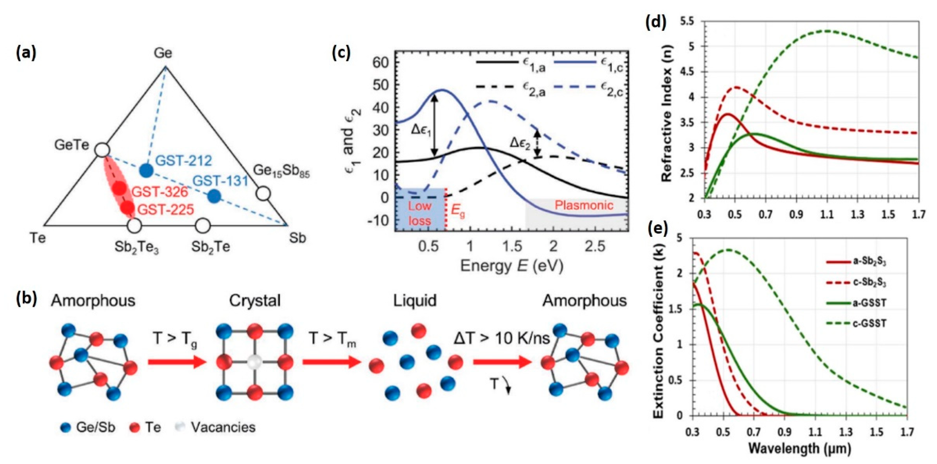
2. Phase Change Materials

PCMs are a special material that exists in at least two different phases, frequently labeled as amorphous and crystalline. These phases are generally a result of rearrangement of the crystal structure of the material [19,20]. Although most other materials do also have amorphous and crystalline phases, the advantage of PCMs lies in the fact that both phases have different crystal structures, bringing about a considerable change in the refractive index [21]. As an example, silicon dioxide does also exist in amorphous and crystalline phases; however, due to their same crystal structure, there is only an insignificant difference in their refractive indices, and it is not regarded as a PCM [21]. On the other hand, octahedral amorphous GST becomes rhombohedral upon switching to crystalline GST [4], leading to a considerable change in refractive index. A contrasting refractive index and reversible switching are the two properties of PCMs that make them useful for optical devices.
While GST remains the most ubiquitous PCM so far [22], there has been research on other materials as a viable alternative platform for various applications. These phase change materials can be divided into four broad categories of chalcogenides, transition metal oxides, organic, and silicon. Some of the important properties of important PCMs from these categories are listed in Table 1. Additionally, some experiments have also been reported using hybrids. Among all these categories, other than some specific requirements for individual applications, for the PCM to be useful for optical devices, it should have the following properties [4,5]:
  • Significant contrast in refractive indices of different phases;
  • Rapid switching;
  • Chemical stability;
  • Reversibly switchable between phases for a large number of cycles.
  • Long cycling endurance, which leads to a large number of cycles.

2.1. Chalcogenides

Chalcogenides are compounds between a chalcogen element (such as sulfur, selenium, tellurium, and polonium) and one or more metals. They generally undergo octahedral to rhombohedral crystalline structure on switching as shown in Figure 1. A typical chalcogenide PCM is GST [30,31], which has many varieties depending upon the concentration of constituent elements, but GST-225 (marked in red in Figure 1a) is the most useful of them all. In addition to GST, there are other chalcogenide PCMs, including GeTe [32], Sb2Te [32], Ag5In5Sb60Te30 (AIST) [33], and GSST [34,35]. These materials exhibit strong resonance bonding in their crystalline state, which is the reason for the considerable difference in the optical properties compared to other materials [36]. Comparisons of GST, GSST, and Sb2S3 properties can be verified in Figure 1c–e. As a group, all of them have small electronegativity differences, which is the reason for their covalent bonding, and both of their phases are nonvolatile at room temperature, which is an advantage for certain applications such as memory devices.
Sb2S3 and Sb2Se3 have been rather late entrants into the group of chalcogenide PCMs. Although some earlier work reported Sb2S3 and Sb2Se3 as PCMs [38,39], subsequent works on chalcogenide PCMs largely ignored these materials [4,32,40] until they were rediscovered as low-loss PCMs [24]. As can be observed in Figure 1c–e, in contrast with GST, which has a large absorption coefficient leading to large losses, Sb2S3 was reported to have an absorption coefficient of zero at the operating wavelength of 1550 nm [24,37], while that of Sb2Se3 was also reported to be near zero at the wavelength of 1550 nm by Delaney [24]. As for the visible region, Sb2S3 still retrains near-zero absorption as opposed to Sb2Se3, which shows a sharper rise in the absorption coefficient [40]. The property of low loss attracted renewed interest in these materials [41,42,43,44,45,46], for both on-chip and free-space applications. On the flip side, Sb2S3 reportedly also undergoes larger size variation when switching from amorphous to the crystalline phase. This may be undesirable for certain applications.
Oxidation of the chalcogenide layer is a major problem among all of these chalcogenide materials which oxidize even at room temperature, leading to performance degradation over time. To prevent oxidation, a protective layer on top of the chalcogenide PCM layer is used. In the case of GST-225 and GSST, the Ge atoms deplete due to oxidation. A thin layer of indium tellurium oxide (ITO) is deposited on top of the GST patch [11] and GSST patch [25] to prevent oxidation. In the case of Sb2S3 and Sb2Se3, a ZnS:SiO2 (20%:80%) layer is used on top which prevents the loss of the sulfur/selenium atom [24]. In some recent publications, Fang and his colleagues reported successfully using a silicon nitride (Si3N4) cap on top of Sb2S3 PCM [47], while Faneca and colleagues also successfully demonstrated the use of an Si3N4 cap on GST [48]. The method seems advantageous concerning the cost of the fabrication process and the complexity of the fabrication process, as deposition of Si3N4 through plasma-enhanced chemical vapor deposition (PECVD) is a standardized practice.

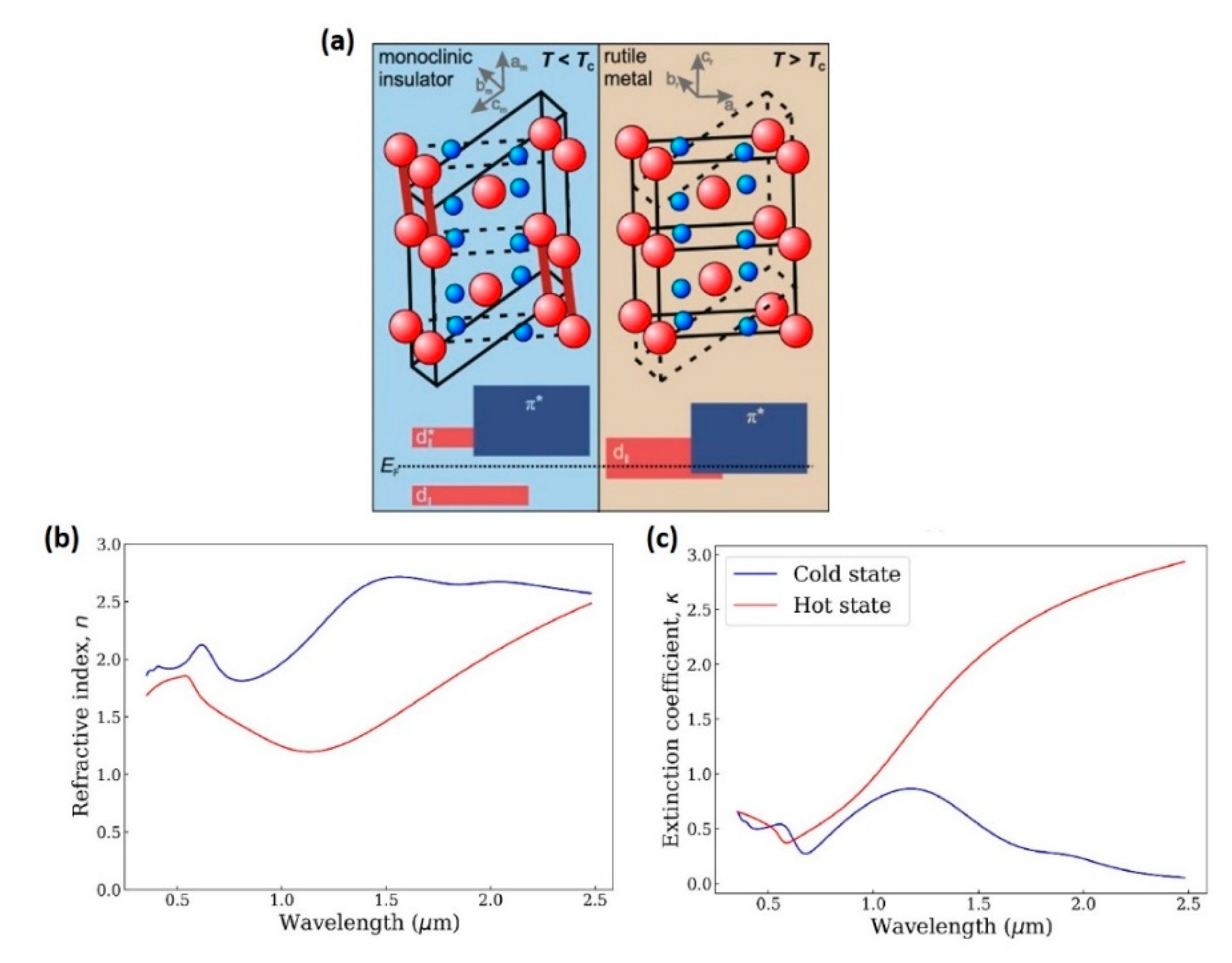
2.2. Transition Metal Oxides

Transition metal oxides that undergo Mott transition (also called correlated materials) are the second most important category of PCMs in terms of volume of publications. Conductivity in Mott insulators such as vanadium dioxide (VO2) is temperature-dependent as they transit from insulator to conductor when the temperature goes from low to high [36]. This transition in conductivity is accompanied by a transition in refractive index, making the materials useful for optical devices. Among them, vanadium oxide is the most popular that can reversibly switch between metallic rutile and two insulating monoclinic structures [49], depicted in Figure 2a. While all of the transition metal oxides show a similar structural transition, the structural transition does not always translate into electronic transition, leading to metallic and insulating phases as in VO2 and NbO2. Both states show different refractive indices and absorption coefficients. Typical values of refractive index and absorption coefficient for VO2 are shown in Figure 2b,c, respectively. The temperature at which the switching takes place is called the transition point. These transition points in the correlated materials can be tuned by tuning the banding filling through doping [50]; for example, the VO2 transition point is at 68 °C, which can be further reduced even to room temperature by doping it with tungsten [36].
The temperature dependence of the metastable states means that the material is suitable for volatile applications. The material has been tested with on-chip devices such as optical switches [53], resonators [19], photonic and plasmonic waveguides [54], polarization converters [55,56]. The temperature can be changed through thermal, electrical, or optical means, but applications requiring faster switching should resort to electrical or optical switching as thermal means are slow.
Like GST, vanadium oxide also readily oxidizes from VO2 to V2O5 in air and, thus, requires a protective layer. Hydrophobic material hafnium dioxide (HfO2) is usually used as the protective layer, which should completely cover the VO2 sample to protect it from oxidation as an unprotected cross-section of the film would also lead to performance degradation [57].
Although many research groups are actively involved in the development of VO2-based devices, some researchers have shown skepticism toward the applicability of VO2-based systems in practical applications for their limited multilevel response, volatility, and complexity of fabrication [58]. This is probably also the reason for them not being as popular as chalcogenides.

2.3. Organic Phase Change Materials
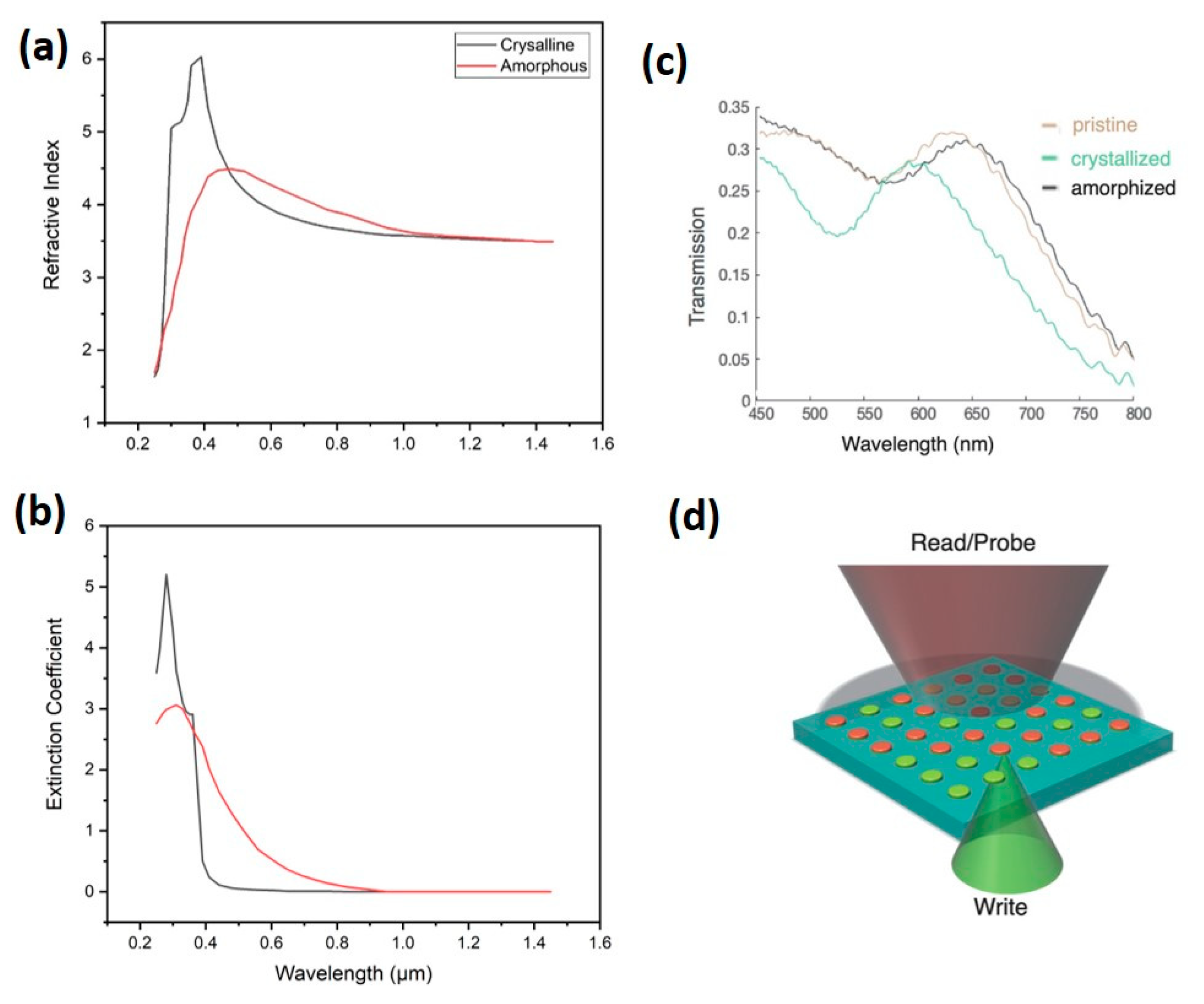
Organic materials are predominantly made of carbon and hydrogen; however, neither these elements nor their compounds inherently exhibit phase change behavior. Therefore, phase change behavior is generally achieved through the interaction of cyclic compounds with other functional groups such as benzene, pyridine, and pyrrole [59]. Some experiments with functional groups containing transition elements have been successful [60].
Numerous organic materials have been used for memristive memory devices [61], switches [62], and neuromorphic computational platforms [63]. This includes pure organic materials in perovskite and non-perovskite forms [63], as well as hybrids with other metals or nonmetals [64,65]. All of these reported devices operate on the basis of a change in resistance through particle transfer leading to a switching action. As this review is focused on phase change materials useful for photonic applications, these platforms are out of the scope of this study.
On the other hand, many organic phase change materials including PNIPAM [66,67] or even doped carbon [59] do exist, which are thermally responsive. As these materials have temperature-dependent metastable states, they can theoretically be used for volatile applications in which VO2 is used. However, to date, there has been no report of using organic phase change materials for optical devices of this nature. We can speculate the reasons to be related to the insufficient contrast in refractive index as reported for PNIPAM [68], phase instability as reported for PNIPAM [69], slower response time [70], or a lack of interest among the research community for exploring organic phase change materials.
Some of the organic phase change materials with different functional groups are shown in Figure 3 with the hope that it could inspire some interest among the research community for organic phase change materials in the future.

2.4. Silicon

Silicon is the most pervasively used material in the photonics industry, as well as the semiconductor industry at large [36], which can also behave as a phase change material. The ability to control the crystallinity of silicon by tuning the temperature during the low-pressure chemical vapor deposition (LPCVD) process has always been known. The transistor industry has been regularly producing crystalline silicon through the action of lasers, both pulsed lasers [71] and excimer lasers [72], in thin films, as well as bulk silicon.
These laser-based systems can crystallize and re-amorphize the silicon on the nanosecond time scale, and this process can be reversibly switched without any deformation. The change in refractive index and absorption coefficient brought about due to the silicon changing phase is not significant at the wavelength of 1.55 µm [73]. However, the difference becomes comparatively large as the wavelength shortens to the visible regime, as shown in Figure 4. Some free-space visible-range proof-of-concept studies have also reported the use of silicon as a PCM [29,74]; however, at the time of writing this review, no demonstration of silicon as a PCM for integrated devices has been found.
Having looked at all four categories of PCMs in detail, the pros and cons of each of the categories for integrated photonic applications are summarized in Table 2.

3. Phase Switching

The phase switching process can be seen at two levels. One is at the atomic level where the kinetics of the phase change process is studied. The other level is at the device level when the phase change is brought about by the designer of the system. The kinetics of crystallization for a phase change material in the amorphous phase can be divided into two categories of nucleation-dominated and growth-dominated [75].
Nucleation-dominated crystallization (shown in Figure 5a) takes place with small spots of crystalline material that are randomly distributed in the PCM. With the rise of the temperature, these nuclei grow until the whole of the PCM has crystallized [76]. A study conducted by Lee and his colleagues [76] found that chalcogenides such as GST crystallize through the nucleation-dominated process where the size distribution of the nuclei depends on the thermal treatment they received, which implies that the statistical status of nuclei distribution in as-deposited amorphous PCM is different to that in pre-annealed PCM. Moreover, their research into the nucleation process also found that, if the amount or volume of subcritical nuclei embedded in amorphous material is greater, the formation of a supercritical nucleus is easier and, thus, the time is shorter [76,77]. The result is that the nucleation process in GST is faster, thus making it a nucleation-dominated crystallization material.
Growth-dominated crystallization (depicted in Figure 5b), on the other hand, is where the rate of growth of the crystalline region is more than the rate of nucleation. In such crystals, only a few nuclei precipitate when the amorphous material is annealed [75]; instead, the precipitated nuclei grow their boundaries to include the still amorphous region into the crystalline region [78]. A study conducted by Khulbe found that, in materials that are growth-dominated, there is a trade-off between incubation time and nucleation speed. The most important examples of materials showing growth-dominated crystallization are Ag and In-doped SbTe (AIST) [75].
At the device level, the underlying physics to achieve switching remains thermal; however, due to the sluggish response of the thermal systems, the PCM is not directly heated. Rather, to switch, either electrical means or optical means are used which achieve the temperature required for switching between crystalline and amorphous phases. Although some electro-thermal methods have also been improved recently through the use of devices such as graphene heaters [79], considered as a fundamental mechanism, there is a lag in switching speed [80]. Among these three means of switching, optical switching produces the fastest switching, followed by electrical switching, while thermal switching remains the slowest [19,36].
Another aspect connected with phase switching is the cycling endurance of the phase change material used for switching. The endurance refers to the number of cycles for which a particular material can be reversibly switched before its two phases (SET and RESET) become difficult to discriminate or the material simply does not switch [81,82]. Such recyclability, measured as the number of cycles of PCMs, is inversely related to the volume of the PCM used, as well as the method of switching adopted. According to Bez, at the fundamental level, there should not be any wear and tear of the material due to switching [83]. However, data show reduced resistive performance after 108–1010 cycles. An interesting finding by Raoux was that the number of cycles and the energy required to trigger the phase transition are inversely related [81]. With respect to the method of switching, GST is known to have a recyclability of higher than 107 cycles when electrically switched, whereas it reduces to 105 cycles when optical switching is employed [84].

3.1. Electrical Switching

Electrical switching is the older of the two methods of electrical and optical switching, and it also finds parallels in earlier technologies such as transistors and other concurrent technologies such as memristors [85,86]. For switching the PCM through electrical means, two different methods have been used. One method is to use an external electrical circuit that is generally connected to a heating element that generates heat through resistance to the current [7,87]. Examples of such systems are ITO heaters [88,89], silver heaters [80], and PIN heaters [90]. The other method is the approach used in memristors where current is used for achieving the phase change [7]. Schematics of the typical arrangements to achieve electrical switching with GST and VO2 as PCMs are shown in Figure 6a–c. The generated heat due to passing current can reversibly switch the state of the PCM unit placed on top of these photonic structures. After switching, when an optical signal passes through the waveguide under the PCM, the signal is evanescently coupled with the straddling PCM unit, leading to a change in the signal. So far, the literature has not revealed any phase change material-based photonic device that has in-line phase change material.
These electrical methods are advantageous, as the heating circuit and the optical circuit of the device are independent and separate from each other. This makes the device more controllable and can enable easier access to complex and multilayered optical circuits. Given that microelectronic technology is well established and mature, it helps in the design of electrically controlled devices. Additionally, as the external control circuitry is also electronic, it can be monolithically integrated. On the other hand, the electronic control circuit makes the devices bulky and increases the steps of fabrication linked to the final cost of the product. However, most importantly as per the current thrust of society toward energy conservation, the electronic method of switching is also wasteful in terms of energy, leading to higher cost per switch. Recently, some graphene-based models have been suggested (schematically shown in Figure 6b) due to their success in limiting the energy waste in electrically controlled PCM-based photonic devices [79,92].

3.2. Optical Switching

Optical switching, also called all-optical devices, on the other hand, is when an optical signal is used to bring about phase change in the PCM. Heat is generated by a high-energy laser pulse due to the opto-thermal effect, leading to switching in the linked phase change material [95]. This can be achieved through two different methods. One method is to use an external laser that is incident on the PCM unit from the far-field and excite it to achieve the switching [82,96]. This method is used for free-space devices, as well as on-chip devices, as shown in Figure 6d. Figure 6d shows that using plasmon polaritons for heat generation would ultimately lead to phase change of the PCM. The second method, which is used for on-chip devices, involves evanescent field coupling. In evanescent coupling, a control signal from a high-powered laser traverses through the on-chip photonic crystal and achieves a switch in the PCM deployed on top through the opto-thermal interaction of the evanescent field and the PCM, as shown in Figure 6e [97]. Although some devices with in-line PCM for certain applications have also been demonstrated [98], the large absorption coefficient in most PCMs currently in use has led to most designers resorting to evanescent coupling (schematically shown in Figure 6e). With the development of low-loss PCMs [41], the phase change material can be deployed in line. The in-line deployed PCM would increase the interaction volume of the PCM and the optical wave, leading to smaller device footprints.
The optical switching uses the same optical circuit that the signal would use, making the device design less bulky while also reducing the number of fabrication steps. Researchers, using optical switching, have reportedly achieved low-power switching using femtosecond lasers [9]. This is a promising result concerning lower energy targets. However, on the other hand, routing the optical signal to achieve the necessary phase change is a difficult task as fabricating three-dimensional photonic circuits is still not easily achievable with the current state of technology. Secondly, achieving switching in the traditional sense using low-loss PCM is difficult due to the low absorption loss of the material. Thus, accessing each PCM unit serially placed on a single waveguide individually is also problematic. While it may not be needed for certain applications such as those implementing Hebbian learning for artificial synapses [95,99], there are other situations where individual access is needed. This has led to some researchers addressing this problem through the use of novel designs such as grid structures [12] or through the use of wavelength division multiplexing with ring resonators straddling individual PCM unit cells [100]. Although promising, these systems are still far from being useful in practical devices.
On the topic of comparison between electrical switching and optical switching in GST-based silicon photonic switches, Zhang concluded that, for the amorphization process, optical switching is advantageous in terms of speed and energy efficiency. However, as alluded to earlier, for large-scale integration purposes, electrical switching is still advantageous as it does not require a complex routing circuit for the photonic circuit [101].

4. Phase Change Memories

Phase change memories can be regarded as the first and arguably most successful application of phase change materials, with CDs as a forerunner, followed by DVDs and BDs as the most popular tertiary memory devices up until recently [5]. The development of such phase change material-based memories can be traced back to the 1970s [102]. In one such work, Yamada and his colleagues [103] presented direct overwriting at the speed of nanoseconds using GST alloy. Despite the success and the early start, these applications were optically switched and not the on-chip applications of phase change materials.
On the on-chip front, the subsequent decades saw extensive developments in the electrically switched resistance-based phase change memories that were comparable with dynamic random access memory (DRAM), NAND based on not/and (NAND) logic gates [104], flash memory [105], and even a proposal for on-chip optical switches [106]. The high-density memory, presented as nonvolatile phase-change random access memory (PRAM), addressed the speed, scalability, and power consumption issues of DRAM [107,108,109].
The first all-optical on-chip phase change memory was proposed by placing a patch of GST-225 on an Si3N4 ring resonator structure on silica. This was reported in 2012 by Pernice and Bhaskaran [10] (some of the details are shown in Table 3), whose group later also fabricated the sample but presented it as a tunable nanophotonic circuit, which was a building block on the way to creating a memory element [110]. Subsequently, a detailed analysis of the memory device made with a GST-225 patch on an Si3N4 racetrack was presented in 2014, which is shown in Figure 7a [111]. Using the principle of change in absorption of GST [112], they showed that the Q-factor, the resonance wavelength, and the extinction ratio can be used to retrieve the state of GST, which is a memory element that can be switched on “a picosecond timescale” [111]. In a later work, the group demonstrated a multilevel cum multibit storage using multiple ring resonators coupled with a single waveguide, accessible through wavelength division multiplexing (WDM) [113]. The demonstrated device with an operating speed of 800 MHz for the write operation could be improved to the gigahertz level using picosecond pulses. The reported device, with a footprint of 0.25 µm2, demonstrated fast (~500 ps) and low-power readout (480 fJ). This work is unique as it also showed the ability to accurately control the percentage of GST in the crystalline or amorphous state through the intensity of the writing pulse [112]. Using a slightly different architecture, an extensive 512 bit all-optical memory was also demonstrated to store a 16 × 16 bit image in grayscale with 2 bit resolution [100]. The device had a relatively large footprint of 1000 × 2400 µm2, which could be slightly reduced using a silicon substrate instead of Si3N4.
For obvious reasons, the footprint of the micro-ring resonator-based device is comparatively large, and reducing it would enable a device with larger density. In such an attempt, the group of Pernice and Bhaskaran used a patch of GST on top of a straight Si3N4 waveguide as a memory unit [114,117]. The device was able to achieve multi-level memory with 21 different states from a single unit of PCM achieved through partial crystallization of GST using pulse width modulation (PWM) on a low-power pump of 526 mA. Figure 7d,e show the experimental demonstration of state transformations using PWM and random accessing of different levels of memory. As the need for frequent optoelectronic conversion is cumbersome, another study reported using integrated phase-change memory, which combines plasmonics, photonics, and electronics to achieve dual electrical and/or optical switching of multilevel states [115].
All of these devices consume relatively high power owing to the large absorption coefficient of GST. As reducing power consumption is the other major thrust of research on phase-change memories, GSST has been proposed as a unit of photonic integrated memory due to its lower absorption [25] and because electro-thermal switching is used for this device.
Following the successful demonstration of all photonic nonvolatile phase-change memory, some researchers resorted to electrically switched photonic memories for Si-PIC. As discussed earlier, electrical switching does offer some benefits compared to all photonic arrangements. It allows fabricating a micro-ring resonator using polycrystalline silicon as the memory element that is switched using joule heating generated using aluminum electrodes. The device consumes 0.476 pJ and 0.316 pJ for the write and read operations, respectively [118]. A similar technique used an ITO heater for heating and achieved switching in a silicon-based device using GST as the phase change material [119]. To further improve the quality of readout, plasmonics has also been used with electrically switched devices, which allows improving the switching speed and energy efficiency [120].

5. In-Memory and Neuromorphic Computing Using PCM

Neuromorphic computing is a paradigm that aims at emulating the way a brain computes, especially focusing on the property of the brain to carry out low-energy information processing, speedy processing, and complex and sophisticated tasks [121]. To mimic the brain, distributed computing topologies are generally used [122], which tend to emulate the behavior of a brain synapse. These structures, appropriately called “artificial synapses”, have been used for machine learning. Most techniques for the implementation of machine learning rely on backpropagation [123,124] as the method to achieve learning, except for a few [125]. Among those using backpropagation as the method of learning, Hebbian learning algorithms are the most popular [126,127].
Phase change material-based memristors have already been in research for a long time for the implementation of neuromorphic learning and in-memory computing [128,129]. The potential for using PCM-based photonic devices for neural networks including neuromorphic computing was understood right after the first report of PCM-based memory [130]. Since then, the neuromorphic potential of phase change materials has constantly been explored and developed (some of the major contribution in this regard have been outlined in Table 4). The first development in this regard was an all photonic synapse that implemented the Hebbian learning rule to achieve synaptic plasticity, made using multiple GST patches on a straight waveguide developed as a memory, already mentioned above [95,117]. In this device (schematic and scanning electron microscopic (SEM) pictures are shown in Figure 8a,b), the synaptic weight is set by changing the number of optical pulses as the synaptic weight exponentially depends on the number of pulses. Using a pulse of 50 ns at 243 pJ, a 7% change in transmission was achieved corresponding to a synaptic weight of “3”. Subsequently, 100 pulses at 1 MHz would allow the PCM to transition from “3” to “1”, while 1000 pulses would revert the state of the synapse to “0”. The research found that the synaptic weight is strictly dependent on the number of pulses applied. The reported device achieved 11 synaptic weights, which could be further improved to a truly analog system by improved pulse control, thereby improving the signal-to-noise ratio.
Creating a synapse on a single waveguide is very attractive from the point of view of reduced footprint, but the system is very difficult to scale; therefore, to create a network of synapses, a different approach is required. A silicon-based ring resonator with a GST patch is one such candidate that has been used for creating an all-optical synapse [133]. A similar synapse (schematically shown in Figure 8c) was also used to create an integrate-and-fire neuron [23]. As any synaptic network is a dot-product engine, these ring resonators are connected in a network to essentially perform dot-product calculations in the form of multiplication of the input with the neuronal weight [134]. This neural network was trained, using a backpropagation algorithm, to recognize handwritten digits from the MNIST dataset [135], achieving 98.06% accuracy on testing. On the speed and energy efficiency front, the ‘read’ and ‘write’ actions take 500 ps and 1.5 ns for 1 pJ and 4 pJ, respectively, using pulses with a duration of 200 ps. This system was later further improved by better incorporation of wavelength division multiplexing [136] and behavioral modeling [137], which further improved energy and speed performance.
There is an inherent contradiction in the constant pursuit for decreasing the energy consumption of computing devices and having GST, which is a highly absorptive material, as the choice for PCM. Given the contradiction, it is only understandable that researchers are looking for alternative materials. In such an attempt, Volker produced an artificial synapse using GSST instead of GST [25]. For this synapse, they resorted to using an electrical switching method implemented using a tungsten contact instead of an optically switched technique. The neural network, made using of Mach–Zehnder interferometers (MZIs) with GSST on both arms, was trained and tested using MNIST [135] handwritten digits and was able to achieve a high level of accuracy.
Scaling the neural network further, [25] recently presented a synapse, graphical processing unit, and a tensor processing unit that perform in-memory calculations through the network of coupler-based latch circuit using Si3N4 with Sb2S3, as well as GST as the PCM [46]. The network (shown in Figure 8e,f) performs at the maximum data rate of 100 GHz and consumes 0.1 uJ of energy. In another work, the tensor processing unit was implemented using GST on a network of ring resonators [137,138]. The implementation of ring resonators helps in reducing the power consumption as the GST is not directly in contact with the propagating waves. They implement parallel processing for convolutional operation showing a variety of machine learning tasks at 2 tera-MAC operations per second with a modulation speed of more than 13 GHz consuming 17 fJ per MAC. This is thus far the fastest implementation of an all-photonic in-memory computational network. The speed, according to the study, can be further improved by expanding the size of the network to increase the level of parallelization.

6. Phase Change Modulators and Switches

Metasurfaces that are artificially micro/nanostructured in a certain way to perform the function of modulators and switches are important PCM-based integrated photonic devices. Such devices generally contain microstructures that partially or fully contain phase change materials in them. The applications of such metasurfaces in producing switches [87,139,140,141], transmission tuners [91], and modulators [19,142,143,144,145] are ubiquitous, which are generally implemented using either Mach–Zehnder interferometers (MZI) or ring resonators [146]. While the major contributions in PCM-based photonic switches and modulators have been outlined in Table 5, the important features of these switches and modulators as per Abdollahramezani are their low power, high contrast, and fast speed [146]. To achieve these features, other than the design parameters, the device is also dependent upon the fabrication processes adopted. As no method is perfect and each method has its own advantages and disadvantages [147].

6.1. VO2 Metasurfaces

Vanadium dioxide-based on-chip modulators have been around for a bit longer than GST-based devices [142,144]. In these devices (shown in Figure 9), a ring resonator with a small patch of VO2 on the ring is fabricated. The change in temperature causes a change in the phase of VO2, leading to a change in the resonant frequency. An extended such device would yield modulation of 16 dB, which is comparable with MZI. In this device, the temperature is changed using substrate heating. In a subsequent study, the phase change was caused externally by a 532 nm wavelength pump laser, leading to modulation of 10 dB in a ring resonator with a radius of 1.5 µm [143]. The experimental setup and the result of modulation achieved with this arrangement are shown in Figure 9c,d, respectively. On the other hand, a more recent study reported a modulator with an extinction ratio of 25 dB and a low insertion loss of 1.4 dB. This was achieved by using a ring resonator with a VO2 patch, which was thermally tuned through lateral micro-heaters placed beside the waveguide [159].
One bottleneck in the performance of VO2 modulators is that the transverse electric (TE) polarized mode interacts weakly with them compared to the transverse magnetic (TM) mode. Some solutions have been proposed to avoid this problem such as using a vertical slot coupler with VO2 active layer [151], delocalization of mode in a small waveguide [149], and using a modulator coupled with a compact mode converter to improve the modulation [153]. These solutions try to optimize the trade-off between insertion loss and extinction ratio while also keeping the device footprint compact. In one such proposal, a layer of silver was added between the vanadium dioxide layer and the silicon layer. This unique hybrid plasmonic solution could reduce the insertion loss while maintaining a high extinction ratio [154].
As VO2 is transitioned to a metallic state which is lossy for electromagnetic waves upon increasing the temperature, this feature opens up the possibility of using VO2 as a switch in photonic circuits. This was shown by the work of Poon [152]. In this design, to make an effective switch of both TE and TM modes, a narrower silicon waveguide was used, and then it was clad with a VO2 patch on all three sides. This increased the interaction of both TE and TM modes, helping in effective switching [152]. The device reported an extinction ratio of 12 dB and insertion loss of 5 dB. The device is electrically switched, having turn-off times of 350 ns and 750 ns, while not relying on hybrid plasmonic design helps to simplify the fabrication process. This design can be improved by using a two-terminal configuration, which helps in applying a large electric field without suppressing the leakage current, thereby drastically reducing the switch-on time to 2 ns [141].
Some interesting studies have been conducted to study the transition dynamics for improvement of switching time of electrically switched VO2-based devices [160,161] and optically switched VO2-based devices [162,163]. For electrically switched devices, the switching time dominated by a spatially percolated metallic phase [161] is improved by increasing the peak pulse [160]. Similarly, in the case of optically switched devices, the switching time can range from a few nanoseconds to microseconds depending on the incident power [162], and a faster relaxation to insulating state can be achieved by using doped TiO2:Nb substrate [163].

6.2. Chalcogenide Modulators and Switches

VO2-based devices are good for volatile applications requiring reasonably high switching speed, but the states are volatile. On the other hand, as seen earlier, chalcogenide devices show nonvolatile switching, making them useful for nonvolatile applications but at the expense of speed, a bottleneck that has been broken with recent research. Moreover, as maintaining the state in a volatile switch may require a constant supply of energy, this may not be a very energy-efficient method of switching. The advantage of only supplying energy when switching is needed instead of a constant supply of energy for maintenance of the state was highlighted in the work of Xu in reports on GST-based electro-optical modulators [14,148]. In the work by the group of Xu on GST [14], a modulator for C-band was presented that is electrically switched, has a footprint of 0.2 µm2, has an extinction ratio larger than 5.4 dB for a switch, and consumes sub-nJ energy per cycle for each switch. This is achieved by a copper-clad 30 nm patch of GST on top of the silicon waveguide. This combination performs better than the various other recipes, such as the silicon–ITO–GST waveguide (shown in Figure 10a) [89] using an ITO heater instead of a copper heater on a straight waveguide, the abovementioned Si–VO2 ring resonator-based modulator [142], Si–GST micro-ring [150], and silicon reverse-biased ring made using oppositely poled silicon and modulated through electrical means.
As silicon suffers from large two-photon absorptions in the near-infrared range, it is considered useful to use silicon nitride instead of silicon for near-infrared devices. For this reason, GST on silicon nitride-based modulators have been a popular subject of research [139,163,164].
However, in general, silicon remains the most frequently used substrate material for on-chip modulation and switching applications based on PCMs. Using GST encapsulated by ITO for electrical switching purposes was also demonstrated by Zhang [7]. In this work, a GST patch was placed on top of a silicon MMI, and switching GST from amorphous to crystalline resulted in transmission contrast of 20 dB over the wavelength range of 1500 nm to 1600 nm. This was achieved using a 20 ns write pulse of 10.4 nJ resulting in GST amorphization, and a 100 ns erase pulse of 9 nJ resulting crystallization of the GST patch. They additionally showed partial crystallization of the GST leading to multiple possible states of crystallization. In separate work, the group also demonstrated the feasibility of using GST-based electrical switching encapsulated by ITO for multiple applications including wavelength division multiplexing and filtering [91]. As also discussed earlier, the interaction region in the straddling PCM is less than an in-line PCM. Placing the GST in line improves the interaction of optical wave and GST, leading to improved switching performance, such as a higher extinction ratio of 33.1 dB and low insertion loss of 0.48 dB for an optical wavelength of 1550 nm [87].
The arrangement of in-line GST for increased interaction has also recently been used for metal–insulator–metal (MIM)-type plasmonic waveguide switches and modulators, where GST is externally switched through pump light [156]. This work investigated three MIM structures such as an end-coupled rectangular resonator, a side-coupled stub resonator, and two mutually coupled resonators. The end-coupled rectangular resonator, the side-coupled stub resonator, and two mutually coupled resonators showed insertion loss of 3.6 dB for fully amorphous and 13.8 dB for crystalline, 16.8 dB for fully amorphous and 2.4 dB for fully crystalline, and 2.6 dB for fully amorphous and 17 dB for fully crystalline states, respectively. The modulation depth reported for these three structures was 13.8 dB, 14.4 dB, and 14.4 dB, respectively, with a switching speed of 500 ps. This modulation depth is intermediate among that achieved in similar work such as Haddadpour’s magneto-optical switch [164] and Piao’s Fano transparency controlled switching [165].
Another method to produce a sort of hybrid between an in-line and a matched PCM layer was introduced by Liang, whereby a 10 nm GST layer was sandwiched between two doped silicon layers in an arrangement also called “anti-slot” [166]. The author simulated electrically switched switches and modulators for an operating wavelength of 2.1 μm and was able to numerically validate an MZI with a device length of 38 μm and insertion loss of −16 dB, while achieving a state transition time of less than 100 ns. In subsequent work, the group also numerically demonstrated modulation of 2.1 μm wavelength using 2 × 2 devices along with one- and two-island waveguides between them [167].
Power consumption in GST-based systems is an important issue, which has led to some researchers exploring other platforms such as Sb2S3 [45,47], Sb2Se3 [158], and GSST [155] for switching and modulation applications. Given that these are newer platforms, there has not been a lot of progress in this direction, but they are promising. The Sb2S3- and GSST-based switches reported lower insertion losses of 0.48 dB and 0.135 dB [47,155], device lengths of 8 µm and 5 µm, and extinction ratios of 30 dB and 20 dB, respectively. Sb2Se3-based modulators using ring resonators as the basic structure demonstrated an insertion loss of 0.45 dB and switching energy of 185 nJ for an electrically switched device [158].
The low-loss nature of these platforms has also encouraged nonconventional applications for PCMs such as MMI switches [45]. On the other hand, GST-based novel designs have also been proposed, which tend to address the power consumption issue of GST-based devices, producing ultra-low-power nonvolatile switches, by using a GST-filled slot instead of using a GST patch for the whole width of the waveguide. The proposed design (shown in Figure 10c,f) is electrically switched and can reach an extinction ratio of 17 dB at 1550 nm with a high energy efficiency of 64 aJ/nm3 for the crystallization and amorphization transitions [98]. However, these are simulation-based results, and whether an actual GST-based device is able to give such a performance in an in-line setting remains to be seen.

7. Discussion and Outlook

Phase change materials are unique in that they drastically change their electrical and optical properties upon the introduction of an external stimulus. Even though these materials have been around for some decades, they have come only recently into focus for designers of on-chip devices. Since the early devices in the early 2010s, a lot of progress has been made in the direction of on-chip PCM-based devices. While most of the progress has been directed toward application in memory devices and neuromorphic computational platforms, a lot of progress has also been made in applications such as switches and modulators. Most of the major contributions in the areas of memory and neuromorphic computing are tabulated in Table 3 and Table 4, while most of the major contributions in switches and modulators are tabulated in Table 5.
GST has by far been the most successful phase change material in terms of acceptability among the research community. This has led to the use of GST in every possible conventional application of PCMs including memory devices, neuromorphic computational platforms, photonic switches, and modulators, which have been implemented using electrical switching, as well as optical switching. While optical switching methods are difficult to scale at present due to the difficulties in the routing of control signals and data signals, electrical switching methods overcome these issues due to inherent differentiation in the routing circuits for control and data signals.
The increased interest in energy conservation through energy efficiency has led to the exploration of material platforms for PCMs that have a low loss. Among these low-loss material platforms, Sb2Se3, Sb2S3, and GSST are the most prominent materials. GSST is a newer platform while Sb2Se3 and Sb2S3 are old but not forgotten materials. This exploration reintroduced these low-loss chalcogenide phase change materials. Although these low-loss materials improve the energy performance of these applications, they also enhance the horizon of possible applications with the induction of devices such as MMIs and beam splitters into the possible applications of on-chip PCMs. This horizon is expected to further increase in the near future with the possible on-chip demonstration of various computational and beam steering platforms already available for free-space applications but difficult to implement on chip due to the losses of GST. Such applications can be implemented on the on-chip platforms using such low-loss PCMs.
After these chalcogenide materials, the most prevalent material is VO2. Although, in terms of refractive index contrast, it is comparable with GST which could potentially make it a rival technology, its states are volatile and can only be maintained through a continuous supply of energy making them only suitable for volatile applications. Due to this property of VO2, its performance does not fare well with the contemporary energy conservation and energy efficiency frameworks. Earlier, it had the advantage of faster switching over GST, but that advantage is also slipping due to new and improved switching methods for chalcogenide PCMs, which means that, although chalcogenide PCMs need activation of control circuitry at each switch between crystalline and amorphous phase, they are still able to achieve faster switching compared with VO2 devices. Nevertheless, VO2 has still found some applications in switching and modulation, where the performance of VO2-based devices is not better than its chalcogenide-based counterparts.
At present, the research in nonconventional material platforms such as silicon and organic materials is seriously lacking. Although silicon has been demonstratively used in a few applications through poling and doping to achieve contrasting phases, the contrast is small, restricting its possible use in actual devices. On the other hand, organic PCMs have not been used at all in photonic devices. However, given their increasingly successful use in resistance-based applications, it is only a matter of time before they also find their way into on-chip refractive index-based devices. The literature reports both volatile and nonvolatile organic PCMs with demonstrable application in resistance-based memristive memory devices. The volatile category includes materials such as PNIPAMs and PEDOTs, while the nonvolatile category includes materials made from aromatic compounds. While the change of phase in these organic PCMs leads to a change in their resistance, due to the lack of research in this area, it remains to be seen whether the phase change also corroborates with a change in the refractive index. Only those materials which show considerable refractive index contrast will be most useful for photonic applications.
The phase change materials and, thus, the devices based on them are deemed essential for next-generation low-power memory devices and neuromorphic computational platforms. The introduction of low-loss materials will be very helpful in the diversification of possible PCM applications in the future. Such diversification is extremely essential to realize one day a fully functional all-optical computing device of conventional and neuromorphic kind. The current developments in this field are healthy but at a very early stage for the realization of practical devices, implying that there still is a long way to go. The future will hold many more interesting applications of PCMs among those discussed above or even newer material platforms with more interesting properties aligning with the needs of specific applications.

Author Contributions

Conceptualization, M.S.N. and L.Z.; writing—original draft preparation, M.S.N.; writing—review and editing, M.S.N., X.Y., L.L., J.C. and L.Z.; supervision, L.Z.; funding acquisition, L.Z. All authors read and agreed to the published version of the manuscript.

Funding

This research was funded by the National Key Research and Development Program (2019YFB2203200, 2018YFB2201702, 2019YFB1802903), the National Natural Science Foundation of China (NSFC) (62090052, 6207030193), and the Shanghai Municipal Science and Technology Major Project (2017SHZDZX03).

Institutional Review Board Statement

Not applicable.

Informed Consent Statement

Not applicable.

Data Availability Statement

Not applicable.

Conflicts of Interest

The authors declare no conflict of interest.

References

  1. Balanis, C.A. Antenna Theory Analysis and Design. Pdf, 2nd ed.; Wiley Sons Inc.: New York, NY, USA, 1997. [Google Scholar]
  2. Tien, P.K. Light Waves in Thin Films and Integrated Optics. Appl. Opt. 1971, 10, 2395–2413. [Google Scholar] [CrossRef]
  3. Capolino, F. Theory and Phenomena of Metamaterials; Capolino, F., Ed.; CRC Press: Boca Raton, FL, USA, 2017; Volume 8, ISBN 9781315219370. [Google Scholar]
  4. Siegrist, T.; Merkelbach, P.; Wuttig, M. Phase Change Materials: Challenges on the Path to a Universal Storage Device. Annu. Rev. Condens. Matter Phys. 2012, 3, 215–237. [Google Scholar] [CrossRef]
  5. Wang, L.; Tu, L.; Wen, J. Application of phase-change materials in memory taxonomy. Sci. Technol. Adv. Mater. 2017, 18, 406–429. [Google Scholar] [CrossRef] [PubMed]
  6. Singh, M.; Raghuwanshi, S.K.; Srinivas, T. Nanophotonic On-Chip hybrid plasmonic Electro-Optic modulator with phase change materials. Phys. Lett. Sect. A Gen. At. Solid State Phys. 2019, 383, 3196–3199. [Google Scholar] [CrossRef]
  7. Zhang, H.; Zhou, L.; Lu, L.; Xu, J.; Wang, N.; Hu, H.; Rahman, B.M.A.A.; Zhou, Z.; Chen, J. Miniature Multilevel Optical Memristive Switch Using Phase Change Material. ACS Photonics 2019, 6, 2205–2212. [Google Scholar] [CrossRef] [Green Version]
  8. Wang, N.; Zhang, H.; Zhou, L.; Lu, L.; Chen, J.; Rahman, B.M.A. Design of ultra-compact optical memristive switches with GST as the active material. Micromachines 2019, 10, 453. [Google Scholar] [CrossRef] [Green Version]
  9. Ruiz de Galarreta, C.; Carrillo, S.G.C.; Au, Y.-Y.; Gemo, E.; Trimby, L.; Shields, J.; Humphreys, E.; Faneca, J.; Cai, L.; Baldycheva, A.; et al. Tunable optical metasurfaces enabled by chalcogenide Phase-Change materials: From the visible to the THz. J. Opt. 2020, 22, 114001. [Google Scholar] [CrossRef]
  10. Pernice, W.H.P.; Bhaskaran, H. Photonic non-volatile memories using phase change materials. Appl. Phys. Lett. 2012, 101, 171101. [Google Scholar] [CrossRef]
  11. Wang, J.; Wang, L.; Liu, J. Overview of Phase-Change Materials Based Photonic Devices. IEEE Access 2020, 8, 121211–121245. [Google Scholar] [CrossRef]
  12. Feldmann, J.; Stegmaier, M.; Gruhler, N.; Ríos, C.; Bhaskaran, H.; Wright, C.D.; Pernice, W.H.P.P. Calculating with light using a chip-Scale all-Optical abacus. Nat. Commun. 2017, 8, 1256. [Google Scholar] [CrossRef] [Green Version]
  13. Shadmani, A.; Miri, M. Design and Simulation of Dual Polarization GST-On-Silicon Nitride Optical Modulator. In Proceedings of the 2019 27th Iranian Conference on Electrical Engineering (ICEE), Yazd, Iran, 30 April–2 May 2019. [Google Scholar]
  14. Yu, Z.; Zheng, J.; Xu, P.; Zhang, W.; Wu, Y. Ultracompact Electro-Optical Modulator-Based Ge 2 Sb 2 Te 5 on Silicon. IEEE Photonics Technol. Lett. 2018, 30, 250–253. [Google Scholar] [CrossRef]
  15. Ghosh, R.R.; Bhardwaj, P.; Dhawan, A. Numerical modeling of integrated electro-Optic modulators based on mode-gap shifting in photonic crystal slab waveguides containing a phase change material. J. Opt. Soc. Am. B 2020, 37, 2287. [Google Scholar] [CrossRef]
  16. Wei, Y.; Zhang, M.; Dai, D. Multichannel mode-selective silicon photonic add/drop multiplexer with phase change material. J. Opt. Soc. Am. B 2020, 37, 3341. [Google Scholar] [CrossRef]
  17. Wang, L.; Lu, S.R.; Wen, J. Recent Advances on Neuromorphic Systems Using Phase-Change Materials. Nanoscale Res. Lett. 2017, 12. [Google Scholar] [CrossRef] [Green Version]
  18. Feldmann, J.; Youngblood, N.; Wright, C.D.; Bhaskaran, H.; Pernice, W.H.P.P. All-Optical spiking neurosynaptic networks with self-learning capabilities. Nature 2019, 569, 208–214. [Google Scholar] [CrossRef] [PubMed] [Green Version]
  19. Miller, K.J.; Haglund, R.F.; Weiss, S.M. Optical phase change materials in integrated silicon photonic devices: Review. Opt. Mater. Express 2018, 8, 2415. [Google Scholar] [CrossRef]
  20. Yang, Z.; Ramanathan, S. Breakthroughs in photonics 2014: Phase change materials for photonics. IEEE Photonics J. 2015, 7, 1–5. [Google Scholar] [CrossRef]
  21. Ding, F.; Yang, Y.; Bozhevolnyi, S.I. Dynamic Metasurfaces Using Phase-Change Chalcogenides. Adv. Opt. Mater. 2019, 7, 1801709. [Google Scholar] [CrossRef] [Green Version]
  22. Guo, P.; Sarangan, A.M.; Agha, I. A Review of Germanium-Antimony-Telluride Phase Change Materials for Non-Volatile Memories and Optical Modulators. Appl. Sci. 2019, 9, 530. [Google Scholar] [CrossRef] [Green Version]
  23. Chakraborty, I.; Saha, G.; Sengupta, A.; Roy, K. Toward Fast Neural Computing using All-Photonic Phase Change Spiking Neurons. Sci. Rep. 2018, 8, 12980. [Google Scholar] [CrossRef]
  24. Delaney, M.; Zeimpekis, I.; Lawson, D.; Hewak, D.W.; Muskens, O.L. A New Family of Ultralow Loss Reversible Phase-Change Materials for Photonic Integrated Circuits: Sb2S3 and Sb2Se3. Adv. Funct. Mater. 2020, 30, 2002447. [Google Scholar] [CrossRef]
  25. Miscuglio, M.; Meng, J.; Mehrabian, A.; Sorger, V.; Yesiliurt, O.; Prokopeva, L.; Kildishev, A.; Zhang, Y.; Hu, J. Artificial Synapse with Mnemonic Functionality using GSST-based Photonic Integrated Memory. Appl. Comput. Electromagn. Soc. 2021, 35, 1447–1449. [Google Scholar] [CrossRef]
  26. Currie, M.; Mastro, M.A.; Wheeler, V.D. Characterizing the tunable refractive index of vanadium dioxide. Opt. Mater. Express 2017, 7, 1697. [Google Scholar] [CrossRef]
  27. Green, M.A. Self-consistent optical parameters of intrinsic silicon at 300K including temperature coefficients. Sol. Energy Mater. Sol. Cells 2008, 92, 1305–1310. [Google Scholar] [CrossRef]
  28. Aspnes, D.E.; Studna, A.A. Dielectric functions and optical parameters of Si, Ge, GaP, GaAs, GaSb, InP, InAs, and InSb from 1.5 to 6.0 eV. Phys. Rev. B 1983, 27, 985–1009. [Google Scholar] [CrossRef]
  29. Wang, L.; Eliceiri, M.; Deng, Y.; Rho, Y.; Shou, W.; Pan, H.; Yao, J.; Grigoropoulos, C.P. Fast Reversible Phase Change Silicon for Visible Active Photonics. Adv. Funct. Mater. 2020, 30, 1910784. [Google Scholar] [CrossRef] [Green Version]
  30. Kalikka, J.; Akola, J.; Jones, R.O. Simulation of crystallization in Ge2 Sb2 Te5: A memory effect in the canonical phase-Change material. Phys. Rev. B Condens. Matter Mater. Phys. 2014, 90, 1–9. [Google Scholar] [CrossRef] [Green Version]
  31. Skelton, J.M.; Pallipurath, A.R.; Lee, T.H.; Elliott, S.R. Atomistic origin of the enhanced crystallization speed and n-type conductivity in Bi-doped Ge-Sb-Te phase-change materials. Adv. Funct. Mater. 2014, 24, 7291–7300. [Google Scholar] [CrossRef] [Green Version]
  32. Lencer, D.; Salinga, M.; Grabowski, B.; Hickel, T.; Neugebauer, J.; Wuttig, M. A map for phase-change materials. Nat. Mater. 2008, 7, 972–977. [Google Scholar] [CrossRef]
  33. Yang, Z.; Li, Y.; Miao, X. Chalcogenide materials for optoelectronic memory and neuromorphic computing. In Photo-Electroactive Nonvolatile Memories for Data Storage and Neuromorphic Computing; Han, S.-T., Zhou, Y., Eds.; Elsevier: Amsterdam, The Netherlands, 2020; pp. 293–315. ISBN 978-0-12-819717-2. [Google Scholar]
  34. Jiang, W. Nonvolatile and ultra-low-loss reconfigurable mode (De)multiplexer/switch using triple-waveguide coupler with Ge2Sb2Se4Te1 phase change material. Sci. Rep. 2018, 8, 15946. [Google Scholar] [CrossRef] [PubMed] [Green Version]
  35. Zhang, Y.; Chou, J.B.; Li, J.; Li, H.; Du, Q.; Yadav, A.; Zhou, S.; Shalaginov, M.Y.; Fang, Z.; Zhong, H.; et al. Broadband transparent optical phase change materials for high-performance nonvolatile photonics. Nat. Commun. 2019, 10, 1–2. [Google Scholar] [CrossRef]
  36. Gong, Z.; Yang, F.; Wang, L.; Chen, R.; Wu, J.; Grigoropoulos, C.P.; Yao, J. Phase change materials in photonic devices. J. Appl. Phys. 2021, 129. [Google Scholar] [CrossRef]
  37. Faneca, J.; Trimby, L.; Zeimpekis, I.; Delaney, M.; Hewak, D.W.; Gardes, F.Y.; Wright, C.D.; Baldycheva, A. On-chip sub-wavelength Bragg grating design based on novel low loss phase-change materials. Opt. Express 2020, 28, 16394. [Google Scholar] [CrossRef]
  38. Vedeshwar, A.; Optical, A.V.; Stibnite, P.; Journal, S.F. Optical Properties of Amorphous and Polycrystalline Stibnite (Sb2S3) Films To cite this version: HAL Id: Jpa-00249371. J. Phys. III 1995, 5, 1161–1172. [Google Scholar]
  39. Kim, J. Optical Disc and Optical Recording Materials. Polym. Sci. Technol. 1996, 7, 646–654. [Google Scholar]
  40. Dong, W.; Liu, H.; Behera, J.K.; Lu, L.; Ng, R.J.H.; Sreekanth, K.V.; Zhou, X.; Yang, J.K.W.; Simpson, R.E. Wide Bandgap Phase Change Material Tuned Visible Photonics. Adv. Funct. Mater. 2019, 29, 1806181. [Google Scholar] [CrossRef] [Green Version]
  41. Faneca, J.; Zeimpekis, I.; Ilie, S.T.; Bucio, T.D.; Grabska, K.; Hewak, D.W.; Gardes, F.Y. Towards low loss non-volatile phase change materials in mid index waveguides. arXiv 2021, arXiv:2101.11127. [Google Scholar]
  42. Mandal, A.; Cui, Y.; McRae, L.; Gholipour, B. Reconfigurable chalcogenide phase change metamaterials: A material, device, and fabrication perspective. J. Phys. Photonics 2021. [Google Scholar] [CrossRef]
  43. Ruiz de Galarreta, C.; Sinev, I.; Alexeev, A.M.; Trofimov, P.; Ladutenko, K.; Garcia-Cuevas Carrillo, S.; Gemo, E.; Baldycheva, A.; Bertolotti, J.; David Wright, C. Reconfigurable multilevel control of hybrid all-dielectric phase-change metasurfaces. Optica 2020, 7, 476–484. [Google Scholar] [CrossRef]
  44. Fang, Z.; Zheng, J.; Majumdar, A. Non-volatile Integrated Photonics enabled by Broadband Transparent Phase Change Material. In Proceedings of the Conference on Lasers and electro-optics, Washington, DC, USA, 10–15 May 2020; p. JTh2B.3. [Google Scholar]
  45. Delaney, M.; Zeimpekis, I.; Du, H.; Yan, X.; Banakar, M.; Thomson, D.J.; Hewak, D.W.; Muskens, O.L. Non-volatile programmable silicon photonics using an ultralow loss Sb2Se3 phase change material. arXiv 2021, arXiv:2101.03623. [Google Scholar]
  46. Yu, T.; Ma, X.; Pastor, E.; George, J.K.; Wall, S.; Miscuglio, M.; Simpson, R.E.; Sorger, V.J. All-Chalcogenide Programmable All-Optical Deep Neural Networks. arXiv 2021, arXiv:2102.10398. [Google Scholar]
  47. Fang, Z.; Zheng, J.; Saxena, A.; Whitehead, J.; Chen, Y.; Majumdar, A. Non-Volatile Reconfigurable Integrated Photonics Enabled by Broadband Low-Loss Phase Change Material. Adv. Opt. Mater. 2021, 2002049, 2002049. [Google Scholar] [CrossRef]
  48. Faneca, J.; Garcia-Cuevas Carrillo, S.; Gemo, E.; de Galarreta, C.R.; Domínguez Bucio, T.; Gardes, F.Y.; Bhaskaran, H.; Pernice, W.H.P.; Wright, C.D.; Baldycheva, A. Performance characteristics of phase-change integrated silicon nitride photonic devices in the O and C telecommunications bands. Opt. Mater. Express 2020, 10, 1778. [Google Scholar] [CrossRef]
  49. Eyert, V. The metal-insulator transitions of VO2: A band theoretical approach. Ann. Phys. 2002, 11, 650–704. [Google Scholar] [CrossRef] [Green Version]
  50. Takami, H.; Kanki, T.; Ueda, S.; Kobayashi, K.; Tanaka, H. Filling-controlled Mott transition in W-doped VO2. Phys. Rev. B 2012, 85, 205111. [Google Scholar] [CrossRef]
  51. Wegkamp, D.; Stähler, J. Ultrafast dynamics during the photoinduced phase transition in VO2. Prog. Surf. Sci. 2015, 90, 464–502. [Google Scholar] [CrossRef] [Green Version]
  52. Guo, P.; Biegler, Z.; Back, T.; Sarangan, A. Vanadium dioxide phase change thin films produced by thermal oxidation of metallic vanadium. Thin Solid Films 2020, 707, 138117. [Google Scholar] [CrossRef]
  53. Miller, K.J.; Hallman, K.A.; Haglund, R.F.; Weiss, S.M. Silicon waveguide optical switch with embedded phase change material. Opt. Express 2017, 25, 26527–26536. [Google Scholar] [CrossRef] [PubMed]
  54. Clark, J.K.; Ho, Y.; Matsui, H.; Delaunay, J. Optically Pumped Hybrid Plasmonic-Photonic Waveguide Modulator Using the VO2 Metal-Insulator Phase Transition. IEEE Photonics J. 2018, 10, 1–9. [Google Scholar] [CrossRef]
  55. Sweatlock, L.A.; Diest, K. Vanadium dioxide based plasmonic modulators. Opt. Express 2012, 20, 8700–8709. [Google Scholar] [CrossRef] [PubMed]
  56. Pouyan, S.M.; Miri, M.; Sheikhi, M.H. Design and numerical analysis of a high-performance optical modulator based on Si-VO2 Bragg grating waveguide. Appl. Opt. 2021, 60, 1083–1091. [Google Scholar] [CrossRef]
  57. Chang, T.; Cao, X.; Li, N.; Long, S.; Zhu, Y.; Huang, J.; Luo, H.; Jin, P. Mitigating Deterioration of Vanadium Dioxide Thermochromic Films by Interfacial Encapsulation. Matter 2019, 1, 734–744. [Google Scholar] [CrossRef] [Green Version]
  58. Pitchappa, P.; Kumar, A.; Prakash, S.; Jani, H.; Venkatesan, T.; Singh, R. Chalcogenide Phase Change Material for Active Terahertz Photonics. Adv. Mater. 2019, 31, 1808157. [Google Scholar] [CrossRef] [PubMed] [Green Version]
  59. Chen, X.; Gao, H.; Xing, L.; Dong, W.; Li, A.; Cheng, P.; Liu, P.; Wang, G. Nanoconfinement effects of N-doped hierarchical carbon on thermal behaviors of organic phase change materials. Energy Storage Mater. 2019, 18, 280–288. [Google Scholar] [CrossRef]
  60. Goswami, S.S.; Matula, A.J.; Rath, S.P.; Hedström, S.; Saha, S.; Annamalai, M.; Sengupta, D.; Patra, A.; Ghosh, S.; Jani, H.; et al. Robust resistive memory devices using solution-processable metal-coordinated azo aromatics. Nat. Mater. 2017, 16, 1216–1224. [Google Scholar] [CrossRef] [PubMed]
  61. Clark, J.; Lanzani, G. Organic photonics for communications. Nat. Photonics 2010, 4, 438–446. [Google Scholar] [CrossRef]
  62. Ding, G.; Wang, Y.; Zhang, G.; Zhou, K.; Zeng, K.; Li, Z.; Zhou, Y.; Zhang, C.; Chen, X.; Han, S.-T. 2D Metal-Organic Framework Nanosheets with Time-Dependent and Multilevel Memristive Switching. Adv. Funct. Mater. 2019, 29, 1806637. [Google Scholar] [CrossRef]
  63. van de Burgt, Y.; Lubberman, E.; Fuller, E.J.; Keene, S.T.; Faria, G.C.; Agarwal, S.; Marinella, M.J.; Alec Talin, A.; Salleo, A. A non-volatile organic electrochemical device as a low-voltage artificial synapse for neuromorphic computing. Nat. Mater. 2017, 16, 414–418. [Google Scholar] [CrossRef]
  64. Gu, C.; Lee, J.-S. Flexible Hybrid Organic–Inorganic Perovskite Memory. ACS Nano 2016, 10, 5413–5418. [Google Scholar] [CrossRef]
  65. Chen, J.; Wang, Z.; Wang, Y.; Zhou, Y.; Han, S.-T. Perovskites for phototunable memories and neuromorphic computing. In Photo-Electroactive Nonvolatile Memories for Data Storage and Neuromorphic Computing; Elsevier: Amsterdam, The Netherlands, 2020; pp. 279–292. ISBN 9780128197172. [Google Scholar]
  66. Cho, E.C.; Kim, Y.D.; Cho, K. Thermally responsive poly (N-isopropylacrylamide) monolayer on gold: Synthesis, surface characterization, and protein interaction/adsorption studies. Polym. Guildf 2004, 45, 3195–3204. [Google Scholar] [CrossRef]
  67. Nash, M.E.; Carroll, W.M.; Nikoloskya, N.; Yang, R.; Connell, C.O.; Gorelov, A.V.; Dockery, P.; Liptrot, C.; Lyng, F.M.; Garcia, A.; et al. Straightforward, one-step fabrication of ultrathin thermoresponsive films from commercially available pNIPAm for cell culture and recovery. ACS Appl. Mater. Interfaces 2011, 3, 1980–1990. [Google Scholar] [CrossRef]
  68. Garner, B.W.; Cai, T.; Ghosh, S.; Hu, Z.; Neogi, A. Refractive Index Change Due to Volume-Phase Transition in Polyacrylamide Gel Nanospheres for Optoelectronics and Bio-photonics. Appl. Phys. Express 2009, 2, 057001. [Google Scholar] [CrossRef]
  69. Aleksandrova, R.; Philipp, M.; Müller, U.; Rioboo, R.J.; Ostermeyer, M.; Sanctuary, R.; Müller-Buschbaum, P.; Krüger, J.K. Phase instability and molecular kinetics provoked by repeated crossing of the demixing transition of PNIPAM solutions. Langmuir 2014, 30, 11792–11801. [Google Scholar] [CrossRef] [PubMed]
  70. Depa, K.; Strachota, A.; Šlouf, M.; Hromádková, J. Fast temperature-responsive nanocomposite PNIPAM hydrogels with controlled pore wall thickness: Force and rate of T-response. Eur. Polym. J. 2012, 48, 1997–2007. [Google Scholar] [CrossRef]
  71. Thompson, M.O.; Mayer, J.W.; Cullis, A.G.; Webber, H.C.; Chew, N.G.; Poate, J.M.; Jacobson, D.C. Silicon Melt, Regrowth, and Amorphization Velocities During Pulsed Laser Irradiation. Phys. Rev. Lett. 1983, 50, 896–899. [Google Scholar] [CrossRef]
  72. Hatano, M.; Moon, S.; Lee, M.; Suzuki, K.; Grigoropoulos, C.P. Excimer laser-induced temperature field in melting and resolidification of silicon thin films. J. Appl. Phys. 1999, 87, 36–43. [Google Scholar] [CrossRef]
  73. Demichelis, F.; Minetti-Mezzetti, E.; Tagliaferro, A.; Tresso, E.; Rava, P.; Ravindra, N.M. Optical properties of hydrogenated amorphous silicon. J. Appl. Phys. 1986, 59, 611–618. [Google Scholar] [CrossRef] [Green Version]
  74. Wang, L.; Rho, Y.; Shou, W.; Hong, S.; Kato, K.; Eliceiri, M.; Shi, M.; Grigoropoulos, C.P.; Pan, H.; Carraro, C.; et al. Programming Nanoparticles in Multiscale: Optically Modulated Assembly and Phase Switching of Silicon Nanoparticle Array. ACS Nano 2018, 12, 2231–2241. [Google Scholar] [CrossRef]
  75. Sarwat, S.G. Materials science and engineering of phase change random access memory. Mater. Sci. Technol. 2017, 33, 1890–1906. [Google Scholar] [CrossRef]
  76. Lee, B.-S.; Shelby, R.M.; Raoux, S.; Retter, C.T.; Burr, G.W.; Bogle, S.N.; Darmawikarta, K.; Bishop, S.G.; Abelson, J.R. Nanoscale nuclei in phase change materials: Origin of different crystallization mechanisms of Ge2Sb2Te5 and AgInSbTe. J. Appl. Phys. 2014, 115, 063506. [Google Scholar] [CrossRef]
  77. Kalb, J.A.; Spaepen, F.; Wuttig, M. Kinetics of crystal nucleation in undercooled droplets of Sb- and Te-based alloys used for phase change recording. J. Appl. Phys. 2005, 98, 054910. [Google Scholar] [CrossRef]
  78. Khulbe, P.K.; Hurst, T.; Horie, M.; Mansuripur, M. Crystallization behavior of Ge-doped eutectic Sb_70Te_30 films in optical disks. Appl. Opt. 2002, 41, 6220. [Google Scholar] [CrossRef]
  79. Ríos, C.; Zhang, Y.; Shalaginov, M.Y.; Deckoff-Jones, S.; Wang, H.; An, S.; Zhang, H.; Kang, M.; Richardson, K.A.; Roberts, C.; et al. Multi-Level Electro-Thermal Switching of Optical Phase-Change Materials Using Graphene. Adv. Photonics Res. 2021, 2, 2000034. [Google Scholar] [CrossRef]
  80. Wang, Y.; Landreman, P.; Schoen, D.; Okabe, K.; Marshall, A.; Celano, U.; Wong, H.-S.P.; Park, J.; Brongersma, M.L. Electrical tuning of phase-change antennas and metasurfaces. Nat. Nanotechnol. 2021. [Google Scholar] [CrossRef] [PubMed]
  81. Raoux, S.; Burr, G.W.; Breitwisch, M.J.; Rettner, C.T.; Chen, Y.-C.; Shelby, R.M.; Salinga, M.; Krebs, D.; Chen, S.-H.; Lung, H.-L.; et al. Phase-change random access memory: A scalable technology. IBM J. Res. Dev. 2008, 52, 465–479. [Google Scholar] [CrossRef]
  82. Rudé, M.; Simpson, R.E.; Quidant, R.; Pruneri, V.; Renger, J. Active Control of Surface Plasmon Waveguides with a Phase Change Material. ACS Photonics 2015, 2, 669–674. [Google Scholar] [CrossRef] [Green Version]
  83. Bez, R.; Gleixner, R.J.; Pellizzer, F.; Pirovano, A.; Atwood, G. Phase Change Memory Cell Concepts and Designs. In Phase Change Materials: Science and Applications; Raoux, S., Wuttig, M., Eds.; Springer US: Boston, MA, USA, 2009; pp. 355–380. ISBN 978-0-387-84873-0. [Google Scholar]
  84. Phase Change Materials; Raoux, S.; Wuttig, M. (Eds.) Springer US: Boston, MA, USA, 2009; ISBN 978-0-387-84873-0. [Google Scholar]
  85. Wełnic, W.; Wuttig, M. Reversible switching in phase-change materials. Mater. Today 2008, 11, 20–27. [Google Scholar] [CrossRef]
  86. Au, Y.-Y.; Bhaskaran, H.; Wright, C.D. Phase-change devices for simultaneous optical-electrical applications. Sci. Rep. 2017, 7, 9688. [Google Scholar] [CrossRef] [Green Version]
  87. Zhang, H.; Xu, L.; Chen, J.; Zhou, L.; Rahman, B.M.A.; Wu, X.; Lu, L.; Xu, Y.; Xu, J.; Song, J.; et al. Ultracompact Si-GST Hybrid Waveguides for Nonvolatile Light Wave Manipulation. IEEE Photonics J. 2018, 10, 1–10. [Google Scholar] [CrossRef]
  88. Wu, C.; Yu, H.; Li, H.; Zhang, X.; Takeuchi, I.; Li, M. Low-Loss Integrated Photonic Switch Using Subwavelength Patterned Phase Change Material. ACS Photonics 2019, 6, 87–92. [Google Scholar] [CrossRef]
  89. Kato, K.; Kuwahara, M.; Kawashima, H.; Tsuruoka, T.; Tsuda, H. Current-driven phase-change optical gate switch using indium–tin-oxide heater. Appl. Phys. Express 2017, 10, 072201. [Google Scholar] [CrossRef]
  90. Zheng, J.; Fang, Z.; Wu, C.; Zhu, S.; Xu, P.; Doylend, J.K.; Deshmukh, S.; Pop, E.; Dunham, S.; Li, M.; et al. Nonvolatile Electrically Reconfigurable Integrated Photonic Switch Enabled by a Silicon PIN Diode Heater. Adv. Mater. 2020, 32, 1–8. [Google Scholar] [CrossRef]
  91. Zhang, H.; Zhou, L.; Xu, J.; Wang, N.; Hu, H.; Lu, L.; Rahman, B.M.A.; Chen, J. Nonvolatile waveguide transmission tuning with electrically-driven ultra-small GST phase-change material. Sci. Bull. 2019, 64, 782–789. [Google Scholar] [CrossRef] [Green Version]
  92. Zheng, J.; Zhu, S.; Xu, P.; Dunham, S.; Majumdar, A. Modeling Electrical Switching of Nonvolatile Phase-Change Integrated Nanophotonic Structures with Graphene Heaters. ACS Appl. Mater. Interfaces 2020, 12, 21827–21836. [Google Scholar] [CrossRef]
  93. Zhao, Z.; Li, J.; Ling, C.; Zhao, X.; Zhao, Y.; Jin, H. Electric field driven abnormal increase in conductivity of tungsten-doped VO2 nanofilms. Thin Solid Films 2021, 725, 138643–doi10. [Google Scholar] [CrossRef]
  94. Varri, V.S.A.; Tripathi, D.; Vyas, H.S.; Agarwal, P.; Hegde, R.S. Optically-reconfigurable phase change material nanoantenna-embedded metamaterial waveguide. Opt. Mater. Express 2021, 11, 988–1003. [Google Scholar] [CrossRef]
  95. Cheng, Z.; Ríos, C.; Pernice, W.H.P.P.; Wright, C.D.; Bhaskaran, H. On-chip photonic synapse. Sci. Adv. 2017, 3, e1700160. [Google Scholar] [CrossRef] [PubMed] [Green Version]
  96. Petronijevic, E.; Sibilia, C. Thin films of phase change materials for light control of metamaterials in the optical and infrared spectral domain. Opt. Quantum Electron. 2020, 52, 110. [Google Scholar] [CrossRef]
  97. Rios, C.; Stegmaier, M.; Cheng, Z.; Youngblood, N.; Wright, C.D.; Pernice, W.H.P.; Bhaskaran, H. Controlled switching of phase-change materials by evanescent-field coupling in integrated photonics [Invited]. Opt. Mater. Express 2018, 8, 2455. [Google Scholar] [CrossRef]
  98. Zhang, J.; Zheng, J.; Xu, P.; Wang, Y.; Majumdar, A. Ultra-low-power nonvolatile integrated photonic switches and modulators based on nanogap-enhanced phase-change waveguides. Opt. Express 2020, 28, 37265. [Google Scholar] [CrossRef] [PubMed]
  99. Ríos, C.; Youngblood, N.; Cheng, Z.; Le Gallo, M.; Pernice, W.H.P.P.; Wright, C.D.; Sebastian, A.; Bhaskaran, H. In-memory computing on a photonic platform. Sci. Adv. 2019, 5, eaau5759. [Google Scholar] [CrossRef] [Green Version]
  100. Feldmann, J.; Youngblood, N.; Li, X.; Wright, C.D.; Bhaskaran, H.; Pernice, W.H.P. Integrated 256 Cell Photonic Phase-Change Memory With 512-Bit Capacity. IEEE J. Sel. Top. Quantum Electron. 2020, 26, 1–7. [Google Scholar] [CrossRef] [Green Version]
  101. Zhang, H.; Yang, X.; Lu, L.; Chen, J.; Rahman, B.M.A.; Zhou, L. Comparison of the phase change process in a GST-loaded silicon waveguide and MMI. Opt. Express 2021, 29, 3503. [Google Scholar] [CrossRef] [PubMed]
  102. Yamada, N. Erasable Phase-Change Optical Materials. MRS Bull. 1996, 21, 48–50. [Google Scholar] [CrossRef]
  103. Yamada, N.; Ohno, E.; Akahira, N.; Nishiuchi, K.; Nagata, K.; Takao, M. High Speed Overwritable Phase Change Optical Disk Material. Jpn. J. Appl. Phys. 1987, 26, 61. [Google Scholar] [CrossRef]
  104. Eilert, S.; Leinwander, M.; Crisenza, G. Phase Change Memory: A New Memory Enables New Memory Usage Models. In Proceedings of the 2009 IEEE International Memory Workshop, Monterey, CA, USA, 10–14 May 2009; pp. 1–2. [Google Scholar]
  105. Simpson, R.E.; Fons, P.; Kolobov, A.V.; Fukaya, T.; Krbal, M.; Yagi, T.; Tominaga, J. Interfacial phase-change memory. Nat. Nanotechnol. 2011, 6, 501–505. [Google Scholar] [CrossRef]
  106. Ikuma, Y.; Saiki, T.; Tsuda, H. Proposal of a small self-holding 2*2 optical switch using phase-change material. IEICE Electron. Express 2008, 5, 442–445. [Google Scholar] [CrossRef] [Green Version]
  107. Zhang, W.; Li, T. Exploring Phase Change Memory and 3D Die-Stacking for Power/Thermal Friendly, Fast and Durable Memory Architectures. In Proceedings of the 2009 18th International Conference on Parallel Architectures and Compilation Techniques, Raleigh, NC, USA, 12–16 September 2009; pp. 101–112. [Google Scholar]
  108. Dong, X.; Jouppi, N.P.; Xie, Y. PCRAMsim: System-level performance, energy, and area modeling for Phase-Change RAM. In Proceedings of the 2009 IEEE/ACM International Conference on Computer-Aided Design-Digest of Technical Papers, San Jose, CA, USA, 2–5 November 2009; pp. 269–275. [Google Scholar]
  109. Lee, B.C.; Ipek, E.; MutIu, O.; Burger, D. Phase change memory architecture and the quest for scalability. Commun. ACM 2010, 53, 99–106. [Google Scholar] [CrossRef]
  110. Rios, C.; Hosseini, P.; Wright, C.D.; Bhaskaran, H.; Pernice, W.H.P. Tunable Nanophotonic circuits based on phase change materials. In Proceedings of the EPCOS Proceedings, Berlin, Germany, 8–10 September 2013. [Google Scholar]
  111. Rios, C.; Hosseini, P.; Wright, C.D.; Bhaskaran, H.; Pernice, W.H.P. On-Chip Photonic Memory Elements Employing Phase-Change Materials. Adv. Mater. 2014, 26, 1372–1377. [Google Scholar] [CrossRef] [Green Version]
  112. Kuramochi, E.; Notomi, M. Optical memory: Phase-change memory. Nat. Photonics 2015, 9, 712–714. [Google Scholar] [CrossRef]
  113. Ríos, C.; Stegmaier, M.; Hosseini, P.; Wang, D.; Scherer, T.; Wright, C.D.; Bhaskaran, H.; Pernice, W.H.P.P.; Rios, C.; Stegmaier, M.; et al. Integrated all-photonic non-volatile multi-level memory. Nat. Photonics 2015, 9, 725–732. [Google Scholar] [CrossRef] [Green Version]
  114. Cheng, Z.; Ríos, C.; Youngblood, N.; Wright, C.D.; Pernice, W.H.P.P.; Bhaskaran, H. Device-Level Photonic Memories and Logic Applications Using Phase-Change Materials. Adv. Mater. 2018, 30, 1802435. [Google Scholar] [CrossRef] [PubMed] [Green Version]
  115. Farmakidis, N.; Youngblood, N.; Li, X.; Tan, J.; Swett, J.L.; Cheng, Z.; Wright, C.D.; Pernice, W.H.P.; Bhaskaran, H. Plasmonic nanogap enhanced phase-change devices with dual electrical-optical functionality. Sci. Adv. 2019, 5, eaaw2687. [Google Scholar] [CrossRef] [PubMed] [Green Version]
  116. Li, X.; Youngblood, N.; Ríos, C.; Cheng, Z.; Wright, C.D.; Pernice, W.H.; Bhaskaran, H. Fast and reliable storage using a 5 bit, nonvolatile photonic memory cell. Optica 2019, 6, 1. [Google Scholar] [CrossRef]
  117. Bhaskaran, H.; Cheng, Z.; Rios, C.A.; Youngblood, N.; Wright, C.D.; Pernice, W.H. On-chip phase-change photonic memory and computing. In Proceedings of the Active Photonic Platforms IX, San Diego, CA, USA, 24 August 2017. [Google Scholar]
  118. Song, J.-F.; Luo, X.-S.; Lim, A.E.-J.; Li, C.; Fang, Q.; Liow, T.-Y.; Jia, L.-X.; Tu, X.-G.; Huang, Y.; Zhou, H.-F.; et al. Integrated photonics with programmable non-volatile memory. Sci. Rep. 2016, 6, 22616. [Google Scholar] [CrossRef]
  119. Taghinejad, H.; Abdollahramezani, S.; Eftekhar, A.A.; Fan, T.; Hosseinnia, A.H.; Hemmatyar, O.; Dorche, A.E.; Gallmon, A.; Adibi, A. ITO-based microheaters for reversible multi-stage switching of phase-change materials: Towards miniaturized beyond-binary reconfigurable integrated photonics. arXiv 2020, arXiv:2003.04097. [Google Scholar]
  120. Gemo, E.; Faneca, J.; Carrillo, S.G.-C.; Baldycheva, A.; Pernice, W.H.P.; Bhaskaran, H.; Wright, C.D. A plasmonically enhanced route to faster and more energy-efficient phase-change integrated photonic memory and computing devices. J. Appl. Phys. 2021, 129, 110902. [Google Scholar] [CrossRef]
  121. Marković, D.; Mizrahi, A.; Querlioz, D.; Grollier, J. Physics for neuromorphic computing. Nat. Rev. Phys. 2020, 2, 499–510. [Google Scholar] [CrossRef]
  122. Miscuglio, M.; Sorger, V.J. Photonic tensor cores for machine learning. Appl. Phys. Rev. 2020, 7, 031404. [Google Scholar] [CrossRef]
  123. Hughes, T.W.; Minkov, M.; Shi, Y.; Fan, S. Training of photonic neural networks through in situ backpropagation and gradient measurement. Optica 2018, 5, 864. [Google Scholar] [CrossRef]
  124. Burr, G.W.; Shelby, R.M.; Sebastian, A.; Kim, S.; Kim, S.; Sidler, S.; Virwani, K.; Ishii, M.; Narayanan, P.; Fumarola, A.; et al. Neuromorphic computing using non-volatile memory. Adv. Phys. X 2017, 2, 89–124. [Google Scholar] [CrossRef]
  125. Tan, J.Y.S.; Cheng, Z.; Li, X.; Youngblood, N.; Ali, U.E.; Wright, C.D.; Pernice, W.H.P.; Bhaskaran, H. Monadic Pavlovian associative learning in a backpropagation-free photonic network. arXiv 2020, arXiv:2011.14709. [Google Scholar]
  126. Song, S.; Miller, K.D.; Abbott, L.F. Competitive Hebbian learning through spike-timing-dependent synaptic plasticity. Nat. Neurosci. 2000, 3, 919–926. [Google Scholar] [CrossRef] [PubMed]
  127. Caporale, N.; Dan, Y. Spike Timing–Dependent Plasticity: A Hebbian Learning Rule. Annu. Rev. Neurosci. 2008, 31, 25–46. [Google Scholar] [CrossRef] [PubMed] [Green Version]
  128. Prezioso, M.; Merrikh-Bayat, F.; Hoskins, B.D.; Adam, G.C.; Likharev, K.K.; Strukov, D.B. Training and operation of an integrated neuromorphic network based on metal-oxide memristors. Nature 2015, 521, 61–64. [Google Scholar] [CrossRef] [Green Version]
  129. Rajendran, B.; Alibart, F. Neuromorphic Computing Based on Emerging Memory Technologies. IEEE J. Emerg. Sel. Top. Circuits Syst. 2016, 6, 198–211. [Google Scholar] [CrossRef]
  130. Wright, C.D.; Au, Y.-Y.; Aziz, M.M.; Bhaskaran, H.; Cobley, R.; Rodriguez-Hernandez, G.; Hosseini, P.; Pernice, W.H.P.; Wang, L. Novel applications possibilities for phase-change materials and devices. In Proceedings of the EPCOS Proceedings, Berlin, Germany, 8–10 September 2013. [Google Scholar]
  131. Wu, C.; Yu, H.; Lee, S.; Peng, R.; Takeuchi, I.; Li, M. Programmable phase-change metasurfaces on waveguides for multimode photonic convolutional neural network. Nat. Commun. 2021, 12, 1–8. [Google Scholar] [CrossRef]
  132. Feldmann, J.; Youngblood, N.; Karpov, M.; Gehring, H.; Li, X.; Stappers, M.; Le Gallo, M.; Fu, X.; Lukashchuk, A.; Raja, A.S.; et al. Parallel convolutional processing using an integrated photonic tensor core. Nature 2021, 589, 52–58. [Google Scholar] [CrossRef] [PubMed]
  133. Zhang, H.; Zhou, L.; Xu, J.; Lu, L.; Chen, J.; Rahman, B.M.A. All-optical synapses based on silicon microring resonators actuated by the phase change material Ge2Sb2Te5. In Proceedings of the Conference on Lasers and Electro-Optics, Washington, DC, USA, 5–10 May 2019; p. STh4H.2. [Google Scholar]
  134. Guo, X.; Xiang, J.; Zhang, Y.; Su, Y. Integrated Neuromorphic Photonics: Synapses, Neurons, and Neural Networks. Adv. Photonics Res. 2021, 2000212. [Google Scholar] [CrossRef]
  135. Deng, L. The MNIST Database of Handwritten Digit Images for Machine Learning Research. IEEE Signal Process. Mag. 2012, 29, 141–142. [Google Scholar] [CrossRef]
  136. Chakraborty, I.; Saha, G.; Roy, K. Photonic In-Memory Computing Primitive for Spiking Neural Networks Using Phase-Change Materials. Phys. Rev. Appl. 2019, 11, 014063. [Google Scholar] [CrossRef] [Green Version]
  137. Carrillo, S.G.C.; Gemo, E.; Li, X.; Youngblood, N.; Katumba, A.; Bienstman, P.; Pernice, W.; Bhaskaran, H.; Wright, C.D. Behavioral modeling of integrated phase-change photonic devices for neuromorphic computing applications. APL Mater. 2019, 7. [Google Scholar] [CrossRef] [Green Version]
  138. Li, X.; Youngblood, N.; Zhou, W.; Feldmann, J.; Swett, J.; Aggarwal, S.; Sebastian, A.; Wright, C.D.; Pernice, W.; Bhaskaran, H. On-chip Phase Change Optical Matrix Multiplication Core. In Proceedings of the 2020 IEEE International Electron Devices Meeting (IEDM), San Francisco, CA, USA, 12–18 December 2020; pp. 7.5.1–7.5.4. [Google Scholar]
  139. Zhou, L.; Zhang, H.; Lu, L.; Chen, J.; Zhou, Z.; Rahman, B.M.A. Ultra-Compact Multi-Level Optical Switching with Non-Volatile GST Phase Change. In Proceedings of the 2019 24th OptoElectronics and Communications Conference (OECC) and 2019 International Conference on Photonics in Switching and Computing (PSC), Fukuoka, Japan, 7–11 July 2019; pp. 1–3. [Google Scholar]
  140. Sanchez, L.; Lechago, S.; Gutierrez, A.; Sanchis, P. Analysis and Design Optimization of a Hybrid VO2/Silicon 2 × 2 Microring Switch. IEEE Photonics J. 2016, 8, 1–9. [Google Scholar] [CrossRef]
  141. Markov, P.; Marvel, R.E.; Conley, H.J.; Miller, K.J.; Haglund, R.F.; Weiss, S.M. Optically Monitored Electrical Switching in VO 2. ACS Photonics 2015, 2, 1175–1182. [Google Scholar] [CrossRef]
  142. Briggs, R.M.; Pryce, I.M.; Atwater, H.A. Compact silicon photonic waveguide modulator based on the vanadium dioxide metal-insulator phase transition. Opt. Express 2010, 18, 11192. [Google Scholar] [CrossRef] [PubMed]
  143. Ryckman, J.D.; Diez-Blanco, V.; Nag, J.; Marvel, R.E.; Choi, B.K.; Haglund, R.F.; Weiss, S.M. Photothermal optical modulation of ultra-compact hybrid Si-VO2 ring resonators. Opt. Express 2012, 20, 13215. [Google Scholar] [CrossRef] [PubMed]
  144. Nag, J.; Ryckman, J.D.; Hertkorn, M.T.; Choi, B.K.; Haglund, R.F., Jr.; Weiss, S.M. Ultrafast Compact Silicon-Based Ring Resonator Modulators Using Metal-Insulator Switching of Vanadium Dioxide; Witzigmann, B., Henneberger, F., Arakawa, Y., Osinski, M., Eds.; SPIE OPTO: San Francisco, CA, USA, 2010. [Google Scholar]
  145. Zheng, J.; Khanolkar, A.; Xu, P.; Colburn, S.; Deshmukh, S.; Myers, J.; Frantz, J.; Pop, E.; Hendrickson, J.; Doylend, J.; et al. GST-on-silicon hybrid nanophotonic integrated circuits: A non-volatile quasi-continuously reprogrammable platform. Opt. Mater. Express 2018, 8, 1551. [Google Scholar] [CrossRef]
  146. Abdollahramezani, S.; Hemmatyar, O.; Taghinejad, H.; Krasnok, A.; Kiarashinejad, Y.; Zandehshahvar, M.; Alù, A.; Adibi, A. Tunable nanophotonics enabled by chalcogenide phase-change materials. Nanophotonics 2020, 9, 1189–1241. [Google Scholar] [CrossRef]
  147. Wang, X.; Qi, H.; Hu, X.; Yu, Z.; Ding, S.; Du, Z.; Gong, Q. Advances in Photonic Devices Based on Optical Phase-Change Materials. Molecules 2021, 26, 2813. [Google Scholar] [CrossRef]
  148. Jain, P.; Tanaka, D.; Tsuda, H. Mach Zehnder interferometer optical switch using phase-change material. In Proceedings of the 2012 International Conference on Photonics in Switching (PS), Ajaccio, France, 11–14 September 2012; pp. 1–3. [Google Scholar]
  149. Kruger, B.A.; Joushaghani, A.; Poon, J.K.S. Design of electrically driven hybrid vanadium dioxide (VO_2) plasmonic switches. Opt. Express 2012, 20, 23598. [Google Scholar] [CrossRef]
  150. Rudé, M.; Pello, J.; Simpson, R.E.; Osmond, J.; Roelkens, G.; van der Tol, J.J.G.M.; Pruneri, V. Optical switching at 1.55 μm in silicon racetrack resonators using phase change materials. Appl. Phys. Lett. 2013, 103, 141119. [Google Scholar] [CrossRef] [Green Version]
  151. Kim, J.T. CMOS-compatible hybrid plasmonic modulator based on vanadium dioxide insulator-metal phase transition. Opt. Lett. 2014, 39, 3997. [Google Scholar] [CrossRef]
  152. Joushaghani, A.; Jeong, J.; Paradis, S.; Alain, D.; Stewart Aitchison, J.; Poon, J.K.S. Wavelength-size hybrid Si-VO2 waveguide electroabsorption optical switches and photodetectors. Opt. Express 2015, 23, 3657. [Google Scholar] [CrossRef]
  153. Diana, L.D.S.; Juan, F.C.; Escutia, A.R.; Kilders, P.S. Ultra-compact electro-absorption VO2–Si modulator with TM to TE conversion. J. Opt. 2017, 19, 035401. [Google Scholar] [CrossRef]
  154. Wong, H.M.K.; Helmy, A.S. Performance Enhancement of Nanoscale VO2 Modulators Using Hybrid Plasmonics. J. Light. Technol. 2018, 36, 797–808. [Google Scholar] [CrossRef] [Green Version]
  155. Song, J.; Ghosh, S.; Zhang, H.; Zhou, L.; Rahman, B.M.A. Design, optimization, and performance evaluation of GSST clad low-loss non-volatile switches. Appl. Opt. 2019, 58, 8687. [Google Scholar] [CrossRef] [PubMed]
  156. Zhang, Z.; Yang, J.; Bai, W.; Han, Y.; He, X.; Zhang, J.; Huang, J.; Chen, D.; Xu, S.; Xie, W. Chipscale plasmonic modulators and switches based on metal–insulator–metal waveguides with Ge2Sb2Te5. J. Nanophotonics 2019, 13, 1. [Google Scholar] [CrossRef] [Green Version]
  157. Faneca, J.; Bucio, T.D.; Gardes, F.Y.; Baldycheva, A. O-band N-rich silicon nitride MZI based on GST. Appl. Phys. Lett. 2020, 116, 093502. [Google Scholar] [CrossRef]
  158. Ríos, C.; Du, Q.; Zhang, Y.; Popescu, C.-C.; Shalaginov, M.Y.; Miller, P.; Roberts, C.; Kang, M.; Richardson, K.A.; Gu, T.; et al. Ultra-compact nonvolatile photonics based on electrically reprogrammable transparent phase change materials. arXiv 2021, arXiv:2105.06010. [Google Scholar]
  159. Jeyaselvan, V.; Pal, A.; Anil Kumar, P.S.; Selvaraja, S.K. Thermally-induced optical modulation in a vanadium dioxide-on-silicon waveguide. OSA Contin. 2020, 3, 132. [Google Scholar] [CrossRef]
  160. Seo, G.; Kim, B.-J.; Ko, C.; Cui, Y.; Lee, Y.W.; Shin, J.-H.; Ramanathan, S.; Kim, H.-T. Voltage-Pulse-Induced Switching Dynamics in $ \hbox{VO}_{2}$ Thin-Film Devices on Silicon. IEEE Electron Device Lett. 2011, 32, 1582–1584. [Google Scholar] [CrossRef]
  161. Jerry, M.; Shukla, N.; Paik, H.; Schlom, D.G.; Datta, S. Dynamics of electrically driven sub-nanosecond switching in vanadium dioxide. In Proceedings of the 2016 IEEE Silicon Nanoelectronics Workshop (SNW), Honolulu, HI, USA, 12–13 June 2016; pp. 26–27. [Google Scholar]
  162. Shibuya, K.; Ishii, K.; Atsumi, Y.; Yoshida, T.; Sakakibara, Y.; Mori, M.; Sawa, A. Switching dynamics of silicon waveguide optical modulator driven by photothermally induced metal-insulator transition of vanadium dioxide cladding layer. Opt. Express 2020, 28, 37188. [Google Scholar] [CrossRef]
  163. Madaras, S.E.; Creeden, J.A.; Lahneman, D.J.; Harbick, A.; Beringer, D.B.; Qazilbash, M.M.; Novikova, I.; Lukaszew, R.A. Dynamics of the blue pump-induced ultrafast insulator-to-metal transition and relaxation in VO2/TiO2 and VO2/TiO2:Nb thin films. Opt. Mater. Express 2020, 10, 1393. [Google Scholar] [CrossRef]
  164. Haddadpour, A.; Nezhad, V.F.; Yu, Z.; Veronis, G. Highly compact magneto-optical switches for metal-dielectric-metal plasmonic waveguides. Opt. Lett. 2016, 41, 4340. [Google Scholar] [CrossRef]
  165. Piao, X.; Yu, S.; Park, N. Control of Fano asymmetry in plasmon induced transparency and its application to plasmonic waveguide modulator. Opt. Express 2012, 20, 18994. [Google Scholar] [CrossRef] [PubMed] [Green Version]
  166. Liang, H.; Soref, R.; Mu, J.; Majumdar, A.; Li, X.; Huang, W.-P. Simulations of Silicon-on-Insulator Channel-Waveguide Electrooptical 2 × 2 Switches and 1 × 1 Modulators Using a Ge2Sb2Te5 Self-Holding Layer. J. Light. Technol. 2015, 33, 1805–1813. [Google Scholar] [CrossRef]
  167. Liang, H.; Soref, R.; Mu, J.; Li, X.; Huang, W.-P. Electro-optical phase-change 2 × 2 switching using three- and four-waveguide directional couplers. Appl. Opt. 2015, 54, 5897. [Google Scholar] [CrossRef] [PubMed]
Figure 1. Chalcogenide phase change materials. (a) Ternary phase diagram of Ge–Sb–Te showing important pseudo-binary combination. Most frequently used (GeTe)x–(Sb2Te3)1-x compounds such as GST-326 and GST-225 are labeled in red. (b) The typical structural transformation in GST-225 when it undergoes a phase transition from amorphous to crystalline to liquid and then back to amorphous. Tg and Tm are the glass transition temperature and melting temperature, respectively. (c) Dielectric function of GST-225 in the amorphous and crystalline phase. (d) Refractive index (n) and (e) extinction coefficient (k) of the amorphous and crystalline state of Sb2S3 and GSST. ((ac) reproduced with permission [21]; (d,e) reproduced with permission [37]).
Photonics 08 00205 g001
Figure 2. Transition metal oxide phase change material VO2. (a) Comparison of monoclinic and rutile crystallographic structures; the unit cells are indicated by solid lines. Vanadium atoms are represented by red balls; oxygen atoms are blue. The electronic band structure near the Fermi level is given at the bottom. (b) Refractive index and (c) extinction coefficient of VO2 in the cold and hot states showing a large change in refractive index and extinction coefficient with the temperature. ((a) reproduced with permission [51]; (b,c) reproduced with permission [52]).
Photonics 08 00205 g002
Figure 3. Optimized organic bimolecular configurations between different nitrogen species of N-doped hierarchical carbon and PCM molecules with different functional groups such as (a) Pyridinic nitrogen, (b) Pyrrolic nitrogen, (c) Graphitic nitrogen, and (d) Oxidized nitrogen (reproduced with permission [59]).
Photonics 08 00205 g003
Figure 4. (a) Refractive index and (b) extinction coefficient of silicon in the crystalline and amorphous states showing a large change in refractive index and extinction coefficient in the UV and near-UV region, which is reduced to an insignificant difference as it reaches 1.5 µm [27,28]. (c) Transmission spectra of pristine a-Si nanodiscs, crystallized nanodiscs, and re-amorphized nanodiscs with 215 nm in diameter. (d) The conceptual pixel-addressable rewritable metasurface for optical wavefront control. ((c,d) Reproduced with permission [29]).
Photonics 08 00205 g004
Figure 5. Two different kinetics of crystallization: (a) nucleation-dominated crystallization kinetics where there is a random distribution of islands of crystallinity that later expand; (b) growth-dominated crystallization where the initial crystalline precipitate grows to include the rest of the amorphous material.
Photonics 08 00205 g005
Figure 6. Various electrical and optical switching methods. (a) Electrical switching of GST on silicon waveguide using Au electrodes [91]. (b) Electrical switching of GST using Pd electrodes while using a graphene heater (reproduced with permission [92]). (c) Schematic of VO2 devices for electric field-driven metal-to-insulator transition (reproduced with permission [93]). (d) Schematic of PCM heating through control of surface plasmons polaritons with external optical excitation (reproduced with permission [82]). (e) Schematic of optically reconfigurable waveguide. High-power optical pulses are used to change the phase of the GST while low-power read pulses can transmit low or high transmittance values depending on the state of the GST deployed on top; (right) 2D cross-sectional view showing GST deployed on top of Si3N4, which is switched through evanescent coupling [94].
Photonics 08 00205 g006
Figure 7. Implementation of phase change memories. (a) Microscopic image different memory elements. Along the horizontal axis, the waveguide–resonator gap is varied from 0.5 to 1.5 μm with 0.3 μm successive step size. Along the vertical direction, the width of GST varies from 0.5 μm (bottom) to 20 μm (top). (b) Comparison between resonances in the crystalline and amorphous states for different GST widths. The graphs show a relative shift of the central wavelength and the reduction of the Q-factor with broadening of the peaks. (c) ER obtained for different racetrack radii (R) as a function of GST width and state. The highlighted regions correspond to those highlighted in (b), and the lines correspond to the fits obtained using the analytical function for ER. (d) Concept of the dual-pulse programming technique; from left to right, an optical image of the device with a GST photonic memory cell, a magnified image of GST on top of the waveguide, and a schematic cross-section of the completed device [116]. (e) Experimental demonstration of multilevel photonic memory using multi-pulse PWM with 12 different levels in a single device showing the relative change in transmission (ΔTr/Tr0). This is an implementation of a switch for the photonic memory with each level accessed through the multiple identical pulse trains of 10 pulses with p = 30 ns and Ppeak = 1.4 mW. (f) Randomly accessing six levels of a single photonic memory. A multiple identical pulse train is used to reach different levels, with N = 12, p = 20 ns, and Ppeak = 1.6 mW. Each level can be reached with the same pulse train at a determined width (τ0 to τ5) from any previous level, where τ0 = 10 ns, τ1 = 10.5 ns, τ2 = 11 ns, τ3 = 11.5 ns, τ4 = 12.5 ns, and τ5 = 15 ns. The dotted and dashed lines denote the times when optical pulse trains are applied for amorphization and crystallization, respectively. ((ac) reproduced with permission [111]; (d) reproduced under creative commons license from [116], (e,f), reproduced with permission [114]).
Photonics 08 00205 g007
Figure 8. Various recent implementations for photonic neuromorphic computing. (a) Schematic of integrated photonic synapse functionally resembling a biological neural synapse where a waveguide is covered with islands of PCM, forming a connection between the pre-neuron and post-neuron parts of the circuit. The post-neuron section contains a circulator (red circle) used to route the output from the synapse to the postsynaptic region and weight (control signals) from port 1 to synapse. (b) SEM image of the photonic synapse presented in (a). (c) Schematic of a bipolar integrate-and-fire neuron implemented using a GST patch straddling on ring resonators. (d) Timing diagram of the bipolar integrate-and-fire neuron presented in (c) showing integration of membrane potential under various incident pulses. (e) An artificial photonic neuron based on PCM. The weighting mechanism and summation rely on a cascade of Sb2S3–SiN hybrid photonic switches which perform operations equivalent to that of a field-programmable gate array (FPGA). Upon placing PCM on one side of the directional coupler (DC), light is partially configured to the cross state following the material being written (crystalline to amorphous). (f) Nonlinear activation function (NLAF) made with GST patches on a silicon waveguide. Nonlinear variations in refractive index are sensed with TM polarized light. ((a,b) reproduced under creative commons license [95]; (c,d) reproduced under creative commons license [23]; (e,f) reproduced under creative commons license from article in arXiv [46]).
Photonics 08 00205 g008
Figure 9. Photonic modulators and switches using VO2 as the PCM. (a) Schematic of VO2 modulator consisting of a grating coupler, a silicon bus waveguide, and a silicon ring resonator covered with a strip of VO2. The SEM image of the VO2 patch straddling the waveguide is shown on the right. (b) Transmission spectra of the through port at increasing temperatures for the schematic presented in (a). The modes of the same azimuthal order are indicated with diamond-shaped markers. These markers show a temperature-dependent red-shift. (c) Schematic of the measurement setup of a VO2-based optical modulator. The SEM image of the modulator is shown in the inset. (d) Optical transmission from the setup given in (c) before and after the trigger. The spectra show a blue-shift upon exposure to the trigger. ((a,b) reproduced under creative commons license [142]; (c,d) reproduced under creative commons license [143]).
Photonics 08 00205 g009
Figure 10. Switches and modulators based on chalcogenide PCM. (a) Schematic top view and cross-section of GST-based optical switch using current-controlled ITO heaters. (b) Optical transmission spectra of GST-based optical switch shown in (a). The spectra contain the transmission from the switch under different configurations. (c) Schematic of the perspective view of the modulator with GST in a slot. (d) On/off extinction ratio (ER) and the insertion losses of the EA modulator presented in (c). (e) Power penalty of the EA modulator shown in (c) as a function of wavelength along the propagation length. (f) Schematic of the perspective view of the 1 × 2 DC switch. GST is implanted in a slot instead of straddling the waveguide. (g) Coupling length of the maximum transmission in the amorphous state and the insertion loss in the crystalline state as a function of g (the gap size between the waveguides). Transmission spectra at the cross and bar ports for (h) amorphous GST and (i) crystalline GST for the switch presented in (f). ((a,b) reproduced under creative commons license [89]; (ci) reproduced under creative commons license [98]).
Photonics 08 00205 g010
Table 1. Properties of some of the PCMs where complex refractive indices for amorphous and crystalline phases are calculated for the wavelength of 1550 nm. The source of data are from [23] for GST-225, [24] for Sb2S3 and Sb2Se3, [25] for GSST, [26] for VO2, and [27,28,29] for Si.
PCMComplex R.I. (Amorphous)Complex R.I. (Crystalline)Transition Temp.Volatile
GST-2254.6 + 0.18i7.2 + 1.9i600 °CNo
Sb2S32.712 + 0i3.308 + 0i270 °CNo
Sb2Se33.285 + 0i4.050 + 0i200 °CNo
GSST3.325 + 0.00018i5.083 + 0.35i250 °CNo
VO22.75 + 0.4i2.1 + 1.3i68 °CYes
Si3.4858 + 0i3.487 + 0i677 °CNo
Table 2. Summary of pros and cons of PCM categories; the last two columns denote whether there has been a report in the literature concerning the use of each category for any type of photonic application or integrated photonic application.
CategoryProsConsUsed for Photonic app.Used for Integrated Photonic app.
ChalcogenideFast switching, nonvolatileHigh transition temperature, lossy
Transition metal oxideLow transition temperature, volatile, fast switchingRequire constant energy, lossy
OrganicLow transition temperatureLow melting point, slower response, easily combustible××
SiliconEase of fabrication, ease of integration, low lossNo refractive index contrast at IR,
Highest transition temperature
×
Table 3. Major contributions in memory devices.
YearPCMMain FeaturesAll OpticalSpeedFootprintPower
2012 [10]GSTSi3N4 ring resonator with GST patch---
2014 [111]GSTSi3N4 ring resonator with GST patch---
2015 [113]GSTSi3N4 multiple ring resonators with GST patches coupled to a single waveguide500 ps0.25 µm2480 fJ
2018 [114]GSTSi3N4 Photonic Memories and Logic Operations using PWM for switching of PCM.
Logic “OR” and “NAND” implemented
---
2018 [115]GSTSi3N4×505 ns-16 pJ
2021 [25]GSSTPhotonic integrated memory with accuracy up to 93%×<1 ps<4 µm2-
Table 4. Major contributions in neuromorphic/in-memory computational platforms.
YearPCMMain FeaturesAll OpticalSpeedFootprintPower
2017 [117]GSTSi3N4-based synapse, with 21 levels on a single waveguide; Implemented with multiple patches of GST on straight waveguide---
2019 [99]GSTDirect scalar multiplication with a single integrated memory cell;
Matrix multiplication with multiple PCM cells
200 ns-180 pJ
2019 [18]GSTSynapses for supervised and unsupervised self-learning;
Implemented with waveguides and waveguide crossings with PCM on top
200 ns-710 pJ
2020 [100]GST512 bit in-memory computing;
Saves 16 × 16 grayscale image with 2-bit resolution
-1000 × 2400 µm2110 pJ, 200 pJ, 230 pJ, 350 pJ
2021 [131]GSTPhotonic convolutional neural network with photonic computing core through PMMC devices1 kHz--
2021 [46] Sb2S3 and GSTLow-energy artificial synapse
Nonlinear activation function
Accuracy >90%
20 ps-0.1 µJ
2021 [132]GSTIntegrated photonic tensor core for parallel convolutional processing1012 MAC per second-17 fJ/MAC
Table 5. Major contributions in PCM-based photonic switches and modulators.
YearPCMMain FeaturesAll OpticalSpeedFootprintInsertion Loss
2010 [142]VO2Ring resonator-based modulator 1-2 µm, 5 µm2 dB
2012 [143]VO2Ring resonator-based modulator 2-0.28 µm2-
2012 [148]GST2 × 2 MZI-based switch 2-93 × 1.7 μm20.5 dB
2012 [149]VO22 × 2 plasmonic switch 2×10 s kHz5 μm1.5 dB
2013 [150]GSTRing resonator-based switch 2--2.5 dB
2014 [151]VO2Plasmonic modulator×-9.47 μm4.5 dB
2015 [152]VO2Switch 2×500 ns0.3 × 0.5 µm2<3.6 dB
2017 [153]VO2Modulator 2×3 ns6 µm0.3 dB
2017 [89]GSTSwitch 3×-3 µm2 dB
2018 [154]VO2Plasmonic modulators 2×1GHz2 µm21.4 dB/µm
2018 [14]GSTModulator 4×-0.2 µm2<2 dB
2019 [155]GSSTSwitch 2-5 µm0.135 dB
2019 [156]GSTPlasmonic modulator for MIM device 2500 ps120 nm3.6 dB
2020 [98]GSTSwitch with PCM in a slot 2×-0.014 µm2<4 dB
2020 [157]GSTMZI-based 5×≈ns5 µm24 dB
2021 [158]Sb2Se3Ring resonator-based modulator 2800 ns11 µm20.45 dB
1 Operating wavelength: 1250–1450 nm. 2 Operating wavelength: 1550 nm. 3 Operating wavelength: 1525–1625 nm. 4 Operating wavelength: 1530–1650 nm. 5 Operating wavelength: 1260–1320 nm.
Publisher’s Note: MDPI stays neutral with regard to jurisdictional claims in published maps and institutional affiliations.

