1. Introduction
Electronic Digital to Analog Converters (DAC), abbreviated eDAC, are key interfaces from the digital to the analog domain. In high-speed digital optical transmitters, the Digital to Optical (D/O) translation typically comprises power consuming and costly eDAC-based data conversion, followed by analogue optical modulation. In a conventional optical link, eDACs are used to drive multilevel analog signals into the optical modulators. However, it would be advantageous, from the viewpoints of performance, energy efficiency, complexity and cost reduction, to adopt direct Digital to Optical domain (D/O), conversion, eliminating the eDAC intermediaries. This would be particularly useful in future generations along the roadmap of ultra-high-speed photonic interconnects, as eDAC technology is ever more expensive and is becoming increasingly difficult to keep scaling up in datarate, while keeping power dissipation in check and retaining ENOB performance.
It appears that non-incremental improvements in oDAC are pending radical conceptual advances in the underlying all-optical D/A architectures. To alleviate the tough tradeoffs curtailing the evolution of photonic networks, as well as enable reconfigurable photonic interconnects, it would be highly valuable to open up innovative venues for improved tradeoffs, unlocking novel capabilities of agile-switchable format-flexible Optical-DAC (oDAC) based direct D/O conversion.
An oDAC is essentially an optical multilevel constellation generator (e.g., a source of optical PAM4 or PAM8 in one-dimension (1D) or optical QAM constellations in 2D). But unlike conventional eDAC + modulator optical transmitter structures, oDACs should be driven right from the digital input bitstream (preferably generated by state-of-the-art CMOS at low voltage swings), without internally resorting to intermediary electrical multilevel signals, thus, eliminating the problematic ultra-high-speed eDACs. Multiple analog two-level electrical signals, as generated by an array of 1-bit electrical drivers (each driven by a bit of the input codeword) are an integral part of oDAC constitution, as each of these analog two-level signals drives an elementary 1-bit modulation-gate. The optical outputs of the array of 1-bit gates are superposed in a suitable optical field characteristic (phase or amplitude), akin to addition of currents or voltages from elementary electrical sources in an eDAC. In oDACs, the analog summation of elementary sources occurs in the optical domain. This fundamental concept will be clarified once we review and advance beyond state-of-the-art oDAC implementations. Existing and newly-introduced oDACs may be broadly classified as either ‘serial’ or ‘multi-parallel’ (MP), these terms referring to the interconnection topology of the 1-bit elementary modulation gates internal to the oDAC.
The predominant activity in the oDAC research area over the last decade has pertained to ‘serial’ structures, based on partitioning the electrodes of the basic Mach-Zehnder Modulator (MZM). The so-called Segmented Mach-Zehnder Modulator (SEMZM), refs. [
1,
2,
3,
4,
5,
6,
7,
8,
9,
10,
11,
12,
13,
14,
15,
16] breaks up the MZM electrodes pair along the two MZM waveguides into multiple (shorter) electrically isolated segments. Each modulation-segment amounts to an elementary 1-bit modulation gate driven by a separate binary signal. It is the summation of the optical phases contributed by the array of 1-bit segments along the device that generates a multilevel output optical signal (by interference of the optical fields, once the top and bottom output waveguides of the SEMZM are superposed in the output combiner).
As alternatives to the incumbent SEMZM ‘serial’ technology, there have been scant demonstrations, of ‘multi-parallel’ oDAC functionality, arraying in parallel a pair of 1-bit (OOK) [
17,
18,
19] or 2-bit (QPSK) [
20,
21,
22,
23,
24,
25] modulation gates, fed by splitting a common optical source, with their outputs superposed in an optical combiner. These structures are referred to here as Multi-Parallel oDAC (MPoDAC). We further distinguish between Direct Detection (DD) and coherent detection (COH) MPoDAC operational modes. Prior MPoDAC work [
17,
18,
19] solely targeted DD PAM4 based on two parallel OOK EAMs–no solution was offered there for either COH or for higher-order DD oDACs. Conversely, refs. [
20,
21,
22,
23,
24,
25] only target QAM generation-DD PAM is out of scope. Noting that these earlier multi-parallel trailblazing earlier-work MPoDAC structures have not made their way into the mainstream, our main interest is to propose innovative modifications and extensions, revealing an extended MPoDAC family significantly outperforming existing oDACs, flexibly reconfigurable between PAM (DD) or QAM (DD) of variable constellation size. The superior efficiencies and flexibility of this new oDAC architecture indicate that a disruptive shift in research is likely to occur in oDAC architectures, migrating from the serial to the multi-parallel paradigm, in order to meet the challenges of upcoming generations of reconfigurable short-reach interconnects. Such architectural transition would potentially enable improved performance, energy-efficiency and agile-reconfigurability. Notably, most existing SEMZM oDACs, unfortunately, require a
Bbits:
Sbits digital encoder (look-up-table with
B <
S, with
B the number of bits and
S the number of segments). Once current SEMZM designs are made ‘DAC-free’ by eliminating redundant segments (taking
S =
B), which enables operating without the ultra-high-speed power-hungry encoder, the SEMZMs exhibit excessive constellation distortion. To attain the full oDAC energy-efficiency benefit, it is imperative to eliminate the power-hungry encoder, albeit without (or at minimal) distortion penalty.
A highlight of our work is to introduce a Binary-Weighted (BiWgt) sub-class of COH MPMZM using Direct Binary Drives (S = B) for their 1-bit MZMs gates, ‘eating the cake and having it too’: Generating ‘perfect’ COH constellations, encoder-free, at ultra-low power.
The remainder of the paper is structured as follows. In
Section 2 we formulate classifications, specifications and optimization criteria for generic oDAC design.
Section 3 introduces constellation quality measures and critically proposes a new ‘maximin-distance’ methodology for optimizing optical one-directional (1D) constellations.
Section 4 reviews and rigorously models state-of-the-art serial-oDACs (SEMZM), enabling consistent performance benchmarking. In
Section 5 we introduce our contending generalized multi-parallel oDAC architecture, its novel parameterization and efficient photonic integrated circuit (PIC) implementations, assuming usage of MZMs for realizing the 1-bit gates–referring to this favored MZMs-based MPoDAC implementation as Multi-parallel MZM (MPMZM). Furthermore, a generic model is derived for the MPMZM transfer factor for COH and DD operation.
Section 6 derives optimized solutions for ‘perfect’ generation of COH PAM 1D constellations of any order based on MPMZMs. We also propose generation of QAM constellations by IQ nesting of COH PAM 1D MPMZMs. In
Section 7 we develop several variants of DD and COH MPMZMs, optimizing them in particular for PAM4 constellations, comparing our schemes with prior MPoDAC work by Verbist et al. [
17,
18,
19] and Yamazaki and Goh [
20,
21,
22,
23,
24,
25]. We also explain the crucial role played by chirp-free operation in order to mitigate a major source of ISI, as enabled by our MPMZM designs.
Section 8 outlines optical re-programmability capabilities of our introduced MPMZMs, in support of next gen of reconfigurable optical interconnects. Finally,
Section 9 concludes this work.
2. Generic oDACs: Classification, Parameterization, Coding
1-bit gates: To introduce the principle of operation, we briefly consider first the realizations of 1-bit modulation gates used as building blocks (BB) in all considered oDAC types. We introduce two types of 1-bit gates: (i) a BPSK phase modulator, referred to as a Phase Gate (PG). (ii) An intensity on-off-keying modulator (OOK) that will be referred to as an Intensity Gate (IG). Typically, in our MPMZM oDACs, we shall use MZMs to realize either PG or IGs (differing just in the type of two-level analog drive waveforms, bipolar or unipolar, applied to the MZM).
The Transfer Factor (TF) (defined as ratio of output and input complex fields) of an MZM is well-known-expressed here (up to a fixed complex factor and omitting the time-dependence) as:
with|denoting or, i.e., one of two options. Here
denote the respective phases|voltages accrued in the top|bottom waveguides and
are the common (average) and (half-)differential phase components of the pair
. Note that the differential voltage between the two MZM arms is
, thus
, is equal to half the differential phase between the arms, thus
may be viewed (under conditions presently discussed below) as the single-ended RF-induced phase in each arm in a push-pull scheme.
To optimize performance, we impose on our 1-bit gates (as well as on the entire oDAC) the chirp-free requirement, requiring that the total phase of the output field TF of our devices be constant from symbol to symbol and also during the symbol transitions). On, the contrary in case there is chirp, then Inter-Symbol-Interference (ISI) arises due to propagation along the end-to-end electro-optical linear channel (including the electrical drivers and the photodetection system), whenever the transfer function of the channel exhibits nonlinear phase frequency response (e.g., dispersion). When the PG and IG 1-bit gates are implemented as MZMs, to ensure chirp-free operation we require that the common phase
be constant (symbol and time-independent). In particular let us henceforth assume that the common phase is null:
, the underlying assumptions for which are (i): We are not interested in (and we discard) any common structural phase accrued along the two MZM arms, which is common to both arms of the MZM. (ii): there is no constant differential phase bias between the two arms, induced either structurally (by having one arm slightly optically-longer) or electrically (having bias electrodes inducing a constant differential phase shift). Then, using (1), we have
, implying that the top and bottom phases must be antipodal (have identical absolute values and opposite signs at any time):
Evidently, the null common phase, , enabling condition, is a special case of constant common phase, thus the adopted push-pull drive scheme satisfies the chirp-free condition.
Having discussed a generic MZM based 1-bit gate, let us consider such gates in the context of SEMZM or MPMZM oDACs, using the index
s = 1, 2, …,
S to label the
S 1-bit gates used in the MPMZM or SEMZM oDAC. The top|bottom phases of the s-th 1-bit gate may be both expressed in terms of the half-differential phase,
:
It remains to specify the differential phase,
during the
k-th symbol interval in terms of the bit driving the gate (distinguish between PG (BPSK),
, and IG (OOK),
):
In the case of an SEMZM type of oDAC, s labels each of the modulation segments (thus in SEMZM, a gate is a modulation segment), consisting of two partial electrodes, push-pull driven just like the top|bottom electrodes of an MZM in (4). Evidently the segments of an SEMZM are not full 1-bit MZM gates. Rather, each segment is a dual-drive Phase Modulator (PM) (essentially a dual-drive MZM without end couplers). The top|bottom PMs are driven per ‘adopted push-pull’ scheme (4).
Continuing our specification of (4),
there denotes the peak absolute value of voltage of the
s-th gate, and it practically suffices to have all phases bounded by
. Expressed in terms of the backoff, the phases satisfy
. Plugging diff phases from (4) into (1) yields:
Thus, PGs|IGs realized as MZM, driven as outlined above, act as chirp-free BPSK|OOK 1-bit gates, amounting to 1-bit oDACs, constituting building blocks for multi-bit oDACs as discussed next.
In our approach, max-full-scale operation of an MZM-based PG or IG is obtained by taking the peak phase per MZM arm to equal
. At this no-backoff (max-full-scale) (5) then reduces to:
Considering IG 1-bit gates in particular, for max-full-scale OOK generation (no-backoff) the induced phases in the two MZM waveguides (obtained by plugging
into the second line of (4)), are:
Notably, for IGs, our adopted push-pull scheme (7) for phase modulations of the two MZM arms, differs from the conventional Quadrature Bias (QB) scheme customarily used for Intensity Modulation (IM) Direct Detection (IM-DD) MZMs. In the conventional QB approach to OOK modulation over DD links, one MZM arm is structurally or electrically phase-biased to accrue an extra phase of
relative to the other arm (equivalently both arms are electrically phase-biased
, such that their bias phase difference be
)) i.e., the optical lengths of the two arms (in the absence of applied drive voltages) differ by a quarter wavelength. Moreover, the electrical drive waveforms in the QB scheme (in the case of no-backoff-max-full-scale OOK generation), are taken as push-pull bipolar voltages inducing phaseshifts
in the MZM upper (lower) arm. In contrast, in our proposed bias scheme (7) for MZM-based IGs, the drives are push-pull unipolar, and the MZM arms we are not statically biased to differ in phase, but rather the two MZM arms are symmetric (in the absence of applied drive waveforms) in the sense that they have the same static optical lengths. We henceforth refer to our IG phase-bias&drive scheme (4) and (5), as Symmetric Bias (SB), to have it distinguished from conventional Quadrature Bias (QB). In the
Appendix A section we compare the two MZM IG schemes, proving their functional equivalence, and considering additional engineering aspects of the electrical drives for IGs and PGs. The
Appendix A further formally proves that the QB scheme may also be adopted for DD SEMZM oDACs, as an alternative to using the DD SEMZM with our SB type phase-biasing and driving. The
Appendix A further shows that both QB and DB schemes operate chirp-free and may be used as DD 1-bit gates in chirp-free oDACs.
Generally, oDACs taxonomy comprises criteria such as detection method, topology, constellation type, dimensionality, oDAC code, which we now briefly outline in turn:
Detection method: COHerent detection (COH) vs. Direct Detection (DD). We shall see that either of the oDAC types, SEMZMs or MPoDACs, may be configured as transmitters for either for COH or DD reception, using a common PIC for each kind, but modifying the ancillary electronic systems.
Topology: We distinguish between two main oDAC topological architecture types:
- (i)
Serial (SE) structure (the SEMZM): Combining two or more gates in tandem, typically using phase gates in order to additively superpose their phase contributions along the serial optical path.
- (ii)
Multi-Parallel (MP) structure (MPoDAC or MPMZM in particular): Combining the outputs of two or more optical gates in parallel, with their output terminated in a passive optical combiner device to optically interfere (superpose) the output fields of the individual gates.
Constellation type: henceforth, constellation means an optical 1D constellation, i.e., a collection of points along the real-axis (e.g., PAM). We shall also consider 2D constellations in the IQ plane (e.g., QAM). For 1D oDACs, the constellation levels are the coordinates of the constellation points along an axis specified in the optical field domain for COH oDACs, in the optical power domain for DD oDACs (the power and field levels being non-negative). For 2D oDACs, the complex-plane (IQ) constellations are necessarily COH ones, as the constellation points are generally distinguishable by amplitude and phase. Along the respective I and Q axes we have a pair 1D COH constellations, e.g., for a 16QAM 2D constellation we have a pair COH PAM4 constellations. COH PAM means here a bipolar symmetric version of PAM, e.g., {−3E, −E, E, 3E} is COH PAM4 in the optical field domain, whereas {0, I, 2I, 3I} is DD PAM4 in the power (intensity) domain.
Dimensionality: oDAC generated constellations are specified by the integer triplet (D, C, S) where D = 1, 2 designates either a 1D or 2D constellation, C is the constellation size (also called order), e.g., C = 4 for PAM4, C = 16 for 16QAM. The integer S denotes the number of 1-bit gates used in the oDAC PIC structure. Examples: S = 3 for an MPMZM with three parallel paths each comprising a 1-bit driven MZM (used to generate a PAM8 constellation, C = 8), i.e., (D, C, S) = (1, 8, 3); S = 7 for a SEMZM with seven segments (also used to generate a PAM8 constellation), i.e., (D,C,S) = (1, 8, 7). We shall always assume dyadic-sized oDAC constellations (dyadic meaning integer-power-of-two): C = 2B = 4, 8, 16,…. A description equivalent to (D, C, S) is then (D, C, B), with an integer denoting the intrinsic number of bits needed to represent the constellation size, C, in binary notation.
oDAC code: A collection of C binary codewords, each of length S. Each codeword, consisting of a string of S bits, is uniquely (one-to-one) associated with one of the levels of the 1D constellation. In each symbol interval, the codeword bits are input, concurrently, into the 1-bit gate array. The S individual bits of the codeword are used to drive the individual 1-bit gates of the oDAC (one bit of the codeword per gate) to generate one of the C levels of the constellation. Each codeword in turn, when fed into the 1-bit gate array input, uniquely commands a constellation level, thus the S bit codewords may be used as labels distinguishing between the C constellation levels. By definition the oDAC input consists of a parallel binary word comprising these B bits representing the codewords labels or addresses. The S bits of each codeword should not be confused with the B bits representing the possible binary strings, each uniquely labeling each of the constellation levels. The B-bit words are inputs into the oDAC in each symbol interval, whereas the S bit codewords are internally applied during the symbol interval to the oDAC 1-bit gate array. In fact, we have the constraint , i.e., there are two cases:
- (a)
if
S =
B, then the
B-bit word, which is input into the oDAC in each symbol interval, coincide with the codeword, i.e., may be directly used to drive the 1-bit gates. The electrical drives of this oDAC configuration are referred to here as Direct Binary Drives (DBD), (alternatively referred to as Direct Digital Drive in [
8,
26,
27], in the restricted context of an SEMZM), since the
B input bits are simply directly routed to
B 1-bit gates to generate each one of the
levels of the constellation. Such an oDAC with
S = B, as just described, does not require a
B:
S encoder (as the
B input bits are directly applied to drive the same number of 1-bit optical gates) and will be, henceforth, referred to as “Binary Weighted” (BiWgt) oDAC–its 1-bit gates are DBD-fed, eliminating the power-hungry encoder.
- (b)
if S > B, then there is redundancy, as the 1-bit gate array is longer than the intrinsic number of bits, B, needed to uniquely specify the distinct levels. A digital B:S mapper is necessary to generate the S-bit codewords from the B-bit input labels indexing each of the C codewords of the code (and the C levels of the constellation), The B:S mapper, or digital encoder, may either store the code lookup table (LUT) or synthesize it in digital logic, which would be trivial at low speed, but it is power-hungry at ultra-high-speed. In fact, in conventional eDACs of the Thermometer-Weighted (ThWgt) type, the B:S mapper may account for about half the power consumption. Since a major motivation for using an oDAC in lieu of an eDAC + modulator is attaining energy-efficiency, the usage of the redundant S > B mode should be avoided whenever possible. Therefore, BiWgt oDACs are preferable from the viewpoint of energy-efficiency (further enjoying the least complexity and other ancillary advantages, since the 1-bit gates count, S, is reduced down to its lower bound B). In most cases, state-of-the-art oDACs, taking the redundancy away to operate in BiWgt-mode (having S = B) end up impairing constellation quality (equivalently elevates the error rate of the optical link).
In contrast, our novel COH MPoDACs, introduced in
Section 5, will all be of the BiWgt type, thus enjoying the energy-efficiency and simplicity of the BiWgt oDAC family, but we shall see that, unlike SEMZM, they are intrinsically free of constellation impairments.
Code Matrix: The oDAC code, i.e., the collection of C codewords, each having S bits, may be arrayed in a code table or code matrix, B, of size , having the codewords as its rows, denoted , with the transpose (by convention denote column-vectors) and c the codeword index (a pointer to codewords in the code table). The entries , of the B matrix consist of Boolean values, defined to correspond to unipolar|bipolar voltage drives: For DD oDACs ; COH oDACs .
BiWgt oDAC code: For BiWgt oDACs, we have
S =
B and the code matrix is now sized
. We may now use a simple counting code, with its
c-th codeword
, consisting of the bitstring of the binary representation of the code index, c (bits listed from right to left starting from the Least Significant Bit (LSB) on the right to the Most Significant Bit (MSB) on the left). The rows of
B are indexed by
c,
, with
c running as usual from top to bottom, whereas the columns are unconventionally indexed as
with
running from right to left (just as the codeword bits do), and expressing
c in binary representation; then the bits
of
c become the entries in the
c-th row of
B, which is the
c-th codeword with elements:
Examples will clarify it, for the lowest orders of BiWgt oDAC,
S =
B = 2 and
S =
B = 3, the respective counting code matrices are listed below (using the convention that spaces separate entries in a row; semicolons separate rows–thus the codewords are simply separated by semicolons):
As for the corresponding COH codes, those are obtained from the DD codes by the affine mapping
The COH counting codes are obtained from the DD counting codes replacing 0 s by −1 s. Examples:
ThWgt oDAC code: We have seen that
S is lower-bounded by
B. The question is whether there is an upper limit to be practically imposed on
S. It may be proven that there is no added benefit using more than
1-bit gates. Thus,
S is bounded from below and above:
The extreme case still requires a B:S encoder (as all oDACs with S > B do), but its code may be designed for arbitrary constellation generation and in particular for a “perfect” equi-spaced max-full-scale constellation. Such oDAC will be referred to as Thermometer-Weighted (ThWgt). The cost to be incurred in exchange of these benefits of the ThWgt, is that for larger constellation orders, the excessive size of S (which now depends nearly exponentially on the number of bits, B) implies a sharp increase in opto-electronic complexity and footprint, excess power consumption due to the sizable B:S encoder and the oDAC photonic circuit with its high count of 1-bit gate drivers, enhanced cross-talk between the multiple RF lines, timing skews, and additional impairments. Therefore, despite its perfect constellation capability, we deem the ThWgt oDAC configuration undesirable, except for the lowest order PAM4 constellation (C = 4, B = 2).
3. Constellation Specification and Optimization
An optical constellation may be specified for COH detection by its field vector and for DD by its intensity (or power) vector:
where, by convention, any nonlinear function of a vector (e.g., squaring, square-root) is the vector of nonlinear functions. We note that DD constellation specifications are formulated in terms of the target power vector, while internal oDAC analysis is conducted in the field domain. For design purposes the power domain constellation specified in the DD case, is mapped into an underlying field constellation,
. We design our oDACs such that all output complex field values share a common phase and discard it, effectively treating input CW and output fields as real-valued.
DD oDAC analysis and design is formulated in terms of the internal fields required to generate the target
, (which is going to ensure the target
). Actually, it is advantageous to redefine the field and power domain quantities as oDAC I/O transfer factor (TF) ratios of either field amplitude or optical intensity, for COH, and DD respectively, in the relevant field amplitude or power domain:
Henceforth, these real-valued non-negative transfer factors, in the appropriate domain (field amplitude or power) are treated as the constellation levels and collected into constellation vectors, blurring the distinction between the TF of an oDAC and its output constellation:
Note: when the CW input field (or power) is unity, then F and P, coincide with E and I, respectively. Thus, the TFs (13) may be viewed as normalized constellations (constellations henceforth refers to the TFs). Moreover, throughout this work, unless otherwise stated, we assume ideal hypothetical models whereby, excess losses and other non-idealities are absent. Therefore, the ‘constellations’ modelled in this work are idealized, revealing the intrinsic performance (the term intrinsic will be interpreted as ‘assuming ideal lossless conditions’), i.e., our models essentially represent performance limits.
The excess loss, if uniform throughout the oDAC device (not path-dependent), may be modelled by scaling down the intrinsic constellations (13) by the square root of the power excess loss factor.
Therefore, in absence of optical amplification, the intrinsic analysis (lossless assumption) implies that all transfer factors are bounded above by unity:
The first and last element of a constellation (be it in the field or power domain) are referred to as the LSB and MSB, respectively and their difference is defined as the constellation Full-Scale (FS):
Our intrinsic (i.e., idealized) designs will strive to achieve max-full-scale performance:
We shall see that most of our COH designs generate field constellations which are symmetric:
Likewise, many of our DD designs generate power constellations symmetric w.r.t. to the half-full-scale point:
In the max-full-scale case the last equation reads:
Perfect constellations are defined as equi-spaced and max-full-scale:
Examples of useful equi-spaced max-full-scale constellations (perfect) labels dropped for brevity):
For a perfect (max-full scale equi-spaced) constellation, (19), the
C − 1 segments connecting adjacent pairs of levels out of the C levels, are all of lengths
respectively; these are the Nearest-Neighbors (NN) distances–all constant here. Generally, NN distances are obtained as the first differences of successive constellation levels (assuming the levels are sorted in increasing order):
The NN-distances are collected into distance vectors,
For oDAC-based optical transmission applications, we adopt, as Figure of Merit (FOM) for the constellation quality, the constellation minimal-distance (in short min-distance), namely the least of all NN-distances:
Intuitively, this min-distance FOM is a measure of the degree of crowding of the constellation, indicative of transmission error rates (BER or SER)–as it is well known in communication theory. Now that we have selected our performance quantifier, a key objective in every oDAC design will be maximization of the constellation minimal distance over the oDAC parameters. Thus, oDAC design is viewed as a so-called maximin optimization problem for the vector NN-distances, over the oDAC parameters (denoted params):
As for the Constraints, those are posed by the physical oDAC configuration and the nature of its parameters. An additional source of constraints stems from the implicit assumption that the constellation be monotone-increasing, i.e., that its constellation levels (be they field or power) be sorted in increasing order. A bound on the maximin-distance is derived by solving,
The solution is formally hard to derive (as all maximin solutions are) but it is intuitively evident:
Thus, the ‘best’ maximin constellation subject to the fixed LSB and MSB end-points (or the fixed distance FS between them), is an equi-spaced one. The optimal solution (denoted by a hat) is then obtained when the FS is maximized (a condition we referred to as maximin):
We cannot expect better results than those: the perfect oDAC designs, to strive for, are equi-spaced max-full-full-scale:
This suggests a Normalized Figure (NFOM) for any oDAC design in terms of its constellation quality: define the oDAC NFOM (on a linear scale) as follows:
or in dB units,
. Alternative approaches for characterizing oDAC performance may be based on figures of merit ported from the domain of electronic DACs (eDAC). E.g., an oDACs may be characterized by its integral or differential nonlinearity. Unfortunately, such “linearity” figures of merit do not consistently correlate with transmission error rates, which are only loosely correlated with the so-called oDAC linearity (a measure of how closely the actually synthesized constellation resembles an equi-spaced one (preferably also max-full-scale). The constellation quality (maximin-distance and NFOM) is just one criterion to assess oDAC designs by. See
Table 1 for additional (mutually inter-dependent) oDAC design characteristics.
4. Constructive Review of Serial oDACs–Rigorous Modeling of Segmented MZMs (SEMZM)
Figure 1 depicts an exemplary
S = 8 segment ThWgt SEMZM optical structure, aiming to implement oDAC functionality. The contiguous MZM electrodes are partitioned into
S segments. Each segment acts a “partial MZM” with push-pull drive, having its upper and lower electrodes driven by a pair of (variable) voltages preferably antipodal voltages (as shown below). Hypothetically assuming a single segment is electrically driven (the other segments grounded or removed) we would obtain a “partial” MZM modulator with a short electrode pair, inducing just a fraction of the maximally possible peak phase modulation, as attained when all segments are active. When all the segments are modulated in unison, driven by properly synchronized binary signals, the total differential phase along the device may assume a multiplicity of values, inducing, by interference in the output coupler multiple optical amplitude (or power) levels at the device output. Each level is determined by the combination of polarities of the voltages applied to the various segments, as detailed below.
We now proceed to model the SEMZM comprehensively and rigorously, beyond the cursory modeling available in the segmented modulator literature which has been more focused on experimental demonstrations. The SEMZM TF is obtained from the generic MZM TF formally replacing the MZM differential phase in (1), by the sum of the differential phases of each of the segments, and also setting the common phase to null,
, as all segments are push-pull driven for chirp-free operation, in both the COH mode (based on PG-drives) and in the DD mode (based on IG-drives):
where
with
the
s-th bit of the
c-th codeword, assuming in the COH|DD cases the respective Boolean values
. Alternatively, (28) is written highlighting the one-to-one correspondence between oDAC codewords and constellation levels:
This formula referred to here as the
SEMZM equation is equivalent to known results, e.g., [
8,
26,
27], (though we differ in our compact notation). The
C distinct output field levels (collected in the
C elements of the constellation vector,
) are generated by applying in each symbol interval various bit combinations (codewords) to binary-drive each of the
S segment elementary modulators.
The SEMZM design parameters to optimize over are: I. Segments count,
S. II. Push-pull voltage
(taken identical for all segments). III. Segments lengths:
s.t.
, with the total length denoted here
since the used
, is referred to the overall length of all the electrodes. Generally, for either a generic MZM or for a push-pull dual phase-modulator (PM), e.g., a single segment of the SEMZM, of length
, driven at voltage
, the induced phase shift is given by
, where
is the particular “reference” electrode length that
is stated at (
defined as the voltage needed to induce pi-phaseshift in a waveguide with electrodes length
). This generic phaseshift formula is applied to each segment, having
specified relative to an effective aggregate electrode of a reference MZM, of length (denoted
, as we refer
to it) equal to the sum of all segment electrode lengths; we note that the
-length product equals
for all segments (due to the SEMZM waveguides and electrodes cross-sectional invariance) and we further assume
, i.e., a common peak voltage be used for all segments. Under these assumptions the
s-th segment phase is,
,
s = 1, 2, …,
S, thus
(
denotes proportionality). We now derive a useful constraint on the sum of all segment phases (defining
):
In particular,
, i.e., at no backoff, max-full-scale is attained:
We may now readily evaluate the constellation min and max levels (LSB and MSB). For DD, as , the least non-negative field level is evidently nulled out by setting all bits to zero. Thus, the LSB is zero. Since, we then have .
The upper bound of
is attained setting all bits to unity,
, yielding the
MSB:
For the COH SEMZM, the bits are bipolar, . The max total phase is attained (as in the DD case) by setting all bits to equal unity , thus the MSB is again . However, the LSB is now attained by setting all bits negative, (this minimizes ) thus the LSB in the coherent case is negative, antipodal to the MSB.
The LSB and MSB are the min and max of the COH constellation (using
):
To operate either the DD SEMZM or the COH SEMZM at max-full-scale we need to satisfy:
We derive the following bounds on the field constellation levels and full-scales for DD,COH:
A consequence of the phases-sum-constraint,
, (with or without backoff), is that the absolute values of inner products in the SEMZM Equation (29), are bounded:
, thus the sine in compound function
has its domain restricted to the
segment, over which the sine is a monotonic bijection, its inverse function, the arcsine (asin), also being a monotonic bijection. Taking the arcsine of both sides of (29) then yields:
For design purposes, the target constellation vector is always specified in the field domain, as an
vector, even if we aim for a DD constellation, in which case power-domain constellation
would rather specified, with the underlying field constellation indirectly derived from it as
The second equivalent version in (37) is a linear equation in the unknown vector
(the nonlinearity having been lumped into the RHS vector,
). The SEMZM equation, itemized for the two respective COH and DD cases, then reads, in code matrix notation:
Our approach to SEMZM design consists of specifying a target field constellation, selecting the oDAC (or equivalently the code matrix B, arraying the codewords as its rows) then optimizing over the “phases design vector” (s.t. constraint (30)), either by solving , if an exact solution does exist, or by finding an approximate solution by solving the maximin problem (24), with F expressed per first form in (37).
As for code design, it is useful to order the codewords of the code
such that the LSB|MSB level be generated for the first|last codeword:
To fully specify the SEMZM code, it remains to state the remaining
C − 2 codewords. For the thermometer-weighted (ThWgt) SEMZM design, the
c-th codewords (DD and COH) are given by
Example: ThWgt SEMZM for PAM8 generation:
. The COH and DD types variants of the code matrix are the given by these
matrices:
We next prove that for an SEMZM having
C − 1 = 2
B− 1 segments, based on the ThWgt code, when no backoff is used, there exists a unique design enabling to synthesize any desired max-full-scale PAM-
C constellation (the perfect, equi-spaced, max-full-scale constellation in particular). Unfortunately, this flexibility comes with a price tag of prohibitive power consumption and high complexity, due to the excessive number of segments, nearly exponential in oDAC number of bits:
The code matrix for the ThWgt SEMZM is
, i.e., the rows count equals the columns count plus one. Inspection of the first codeword and the last one shows that the first and last equation in the system of linear equations (37)
are redundant, as the first codeword is linearly dependent on other codewords (e.g., inspect the first row of the PAM8 ThWgt SEMZM code matrix for either COH or DD in (37) for definiteness). Once the first equation is discarded, (37) is then reduced to the following system of
C−1 linear equations in
C − 1 unknowns:
Since, for the ThWgt-codes, the reduced matrix,
(obtained from B by discarding the first row) is now square
and has full rank, there is always a solution, formally expressed as
We are not going to write down the solution explicitly, but what matters is the methodology of the proof of existence just carried out, leveraged to prove a new result for SEMZM oDACs with segment count,
S, less than constellation levels number minus one (cf. 40):
Proof: In this case the code matrix B is tall (height < width), and so is the reduced code matrix , which is one unit shorter in height. The linear system of equations is now overdetermined (more equations than unknowns) and there is generally no solution, except in the accidental case when the RHS happens to fall in the column space of .
A key practical limitation is highlighted by our rigorous SEMZM analysis: unfortunately, the most energy efficient BiWgt SEMZM (S = B < 2B − 1 = C − 1), is unable to synthesize arbitrary constellations. In particular perfect max-full-scale equi-spaced constellations are out of reach unless one gives up the BiWgt advantages: the energy-efficiency + low-complexity benefit, upon adopting the ThWgt SEMZM, which is power-hungry and complex (and long, lossy) with excessive number of segments. We may elect a compromise, accepting a tradeoff between constellation quality vs. energy-efficiency + low-complexity, by adopting SEMZM designs with B < S < 2B − 1 (i.e., neither BiWgt nor ThWgt), with more segments, S, than the number of bits, B, but still fewer than the 2B − 1 of them. Along this tradeoff axis, the higher S is, the higher the constellation quality, but the higher the penalties in the power consumption, complexity, footprint and other impairments such as electrical crosstalk, time-skews.
A sizeable portion of the energy-efficiency penalty in redundant designs with more segments than bits (S > B) is due to the need for a high-speed Bbits:Sbits digital encoder, increasingly power-hungry as the ratio S/B increases beyond unity. It is only the BiWgt class of oDACs that eliminates this encoder, but then one must watch out for excessive constellation distortion (reduced min-distance).
4.1. BiWgt SEMZM: Dyadic Electrodes Design and Its Performance
For substantial modulation backoff of about 50% or more, (i.e., the constellation full-scale optical power is at least halved), we may approximate
in (37), reducing the SEMZM equation to:
An analogy may be set up with electronic DACs. The output current levels in a BiWgt eDAC are generated by summing up elementary current sources
which are dyadic-weighted meaning that they form a geometric sequence with ratio 2:
The eDAC electrical output levels come out equi-spaced. Equations (43) and (44) are analogous, with the phases
playing the role of the elementary current sources
. This suggests that in order to generate an equi-spaced constellation with the backed-off SEMZM we should take
. Along with the phases-sum-constraint, (31)
, this implies:
As a common peak voltage is used for all segments, the electrode lengths form a dyadic sequence as well: . Backoff does save power consumption but causes intrinsic modulation loss, as the equi-spaced constellation is compressed relative to its max-full-scale span. If the backoff is reduced or eliminated then the approximation which enabled the dyadic design to yield an equi-spaced constellation is no longer valid. Nevertheless, we prove, in the next subsection, that upon using dyadic phases, the constellation min-distance monotonically increases in the variable. Therefore, by using design (45), albeit at , the constellation min-distance will be seen to increase relative to having .
4.1.1. PAM4 DD SEMZM Dyadic Design Performance
Let us exemplify the dyadic design for 2-bit BiWgt DD SEMZM, namely
C = 4,
B = 2 DD PAM4. The dyadic design, at backoff factor denoted for brevity
, is specified as a 2:1 ratio of phases:
Substituting the four 2-bit codewords above into the field constellation levels expression yields:
Substituting the binary-weighted phase parameter values (46) into this field vector, yields:
The power constellation for
k = 1 (no backoff) is listed below (its min distance is
):
Experimental demonstrations of PAM4 DD typically use substantial backoff of the order of 3 dB (e.g., [
3]). The corresponding
k value is found by solving the equation
, yielding
(indeed, the field TF of a reference MZM is
. This value is also the MSB of the PAM4 constellation, −3 dB down in optical power relative to a max-full-scale constellation). At 3 dB backoff, plugging
into (48), the min-distance is:
This min-distance corresponds to a normalized figure of merit for the 3-dB backed-off configuration:
Comparing this min-dist = 0.067 at 3 dB backoff, with our no-backoff (
k = 1) solution (49) which has min-dist = 0.25, we see that the backoff policy substantially degrades the constellation min-distance. Thus, the ‘common wisdom’ of backing-off the SEMZM ‘to make it linear’ is actually detrimental. To formally prove that the optimal setting is the no-backoff one, let us parameterize the min-distance over the
k variable. Three NN-distances, featuring in (48),
are plotted in
Figure 2. It is apparent that we have
all over the domain (0,1). Thus, the min-distance coincides with
:
The maximum of the min-distance function over
k evidently occurs at the right-end of the (0,1) interval,
k = 1, thus the optimal solution is indeed the one we suggested in (49). Compared with the “perfect” power constellation,
, having min-distance
, the ratio of minimal distances yields the constellation Normalized Figure of Merit (NFOM):
which is 5.62 dB higher than the NFOM (51) at the typical 3 dB backoff.
To recap, we worked out the min-distance of the backed-off constellation maximizing its min-distance over the backoff factor, k, and have shown that the maximin distance occurs at k = 1. The practice of backing off the PAM4 DD SEMZM is a misconception, giving up performance unnecessarily, since having an equi-spaced constellation is irrelevant. From communication-theoretic considerations it follows that the essential factor determining BER is the minimal-distance of the constellation, which is what we have optimized (adopting the conventional dyadic taps design). Therefore, the experimental practice of backing off the PAM4 DD SEMZM is not recommended (unless it is acceptable to sacrifice communication link performance in order to reduce power consumption).
4.1.2. PAM4 COH SEMZM Dyadic Design Performance
We now also work out a coherent version of the dyadic BiWgt 3SE. Still using the dyadic pair of phases,(46)
we adopt the bipolar code,
The four field levels
are now:
The best performance is also obtained at no backoff,
k = 1, plugging into the field vector (54) the same dyadic phase parameter values (46), as used for the DD design,
yielding:
with distances vector and minimal distance given by,
The resulting NFOM of the constellation (see (27)) happens to be the same as in the DD case:
Thus, our proposed no-backoff PAM4 COH design also has an intrinsic insertion loss of −1.25 dB, as the DD design does. This is not accidental, as it may be shown that there is an affine isomorphism between DD and COH SEMZM optimized constellations, but this is going to be treated elsewhere.
5. Multi-Parallel oDACs (MPMZM in Particular)
The previous sections have revealed uneasy tradeoffs in SEMZM serial oDACs, which we aim to relieve by introducing an alternative multi-parallel oDAC (MPoDAC) photonic architecture for 1D constellation generation in optical transmitters, depicted in
Figure 3. This novel oDAC architecture significantly improves the triple tradeoff between oDAC power-consumption (as well as complexity, size, cost) versus constellation quality vs. modulation rate. The
S-way MPoDAC generic photonic structure is seen to feature
S parallel paths comprising elementary oDAC building blocks:
One-bit modulation gates. Light is fanned out, ‘S-way’, by the variable 1: S splitter to feed the S parallel paths (S ≥ 2), each of which are 1-bit modulated and coherently (in phase) superposed in the S:1 optical combiner, which performs optical fan-in to generate a single useful output beam (excess light may emerge and be terminated at other ports of the combiner). In addition, the paths also contain, in tandem to the 1-bit gates, slow tunable phaseshifters, maintaining equal common phases of the optical fields of the parallel paths, at the internal point of superposition inside the optical combiner. This proposed MPoDAC structure may be parameterized (soft-reconfigured) to achieve two types of reception functionality, either COH or DD.
In the favored implementations of our proposed MPoDAC generic structure, we assume MZMs with binary voltage drivers are used for the 1-bit gates in each of the parallel paths. We refer to the resulting MZMs-based MPoDAC, based on MZM 1-bit gates, as Multi-Parallel MZM (MPMZM). The parallelized MZMs are either used as PGs (BPSK modulators requiring bipolar drives) for COH or as IGs (OOK modulators requiring unipolar drives) for DD. Specific examples of the MPMZM photonic layout for PAM8 and PAM4 generation are shown in
Figure 4. A common photonic structure supports either DD or COH constellation generation, the two usage modes sharing the same PIC, just differing in the type of voltage drivers (unipolar or bipolar) for the MZMs in the multiple paths.
Fan-in/fan-out: The variable 1:
S and
S:1 fan-in/out modules in
Figure 3,
Figure 4 may be realized, on photonic integration platforms, as Mode-Converters (MC), assembled out of meshes of slow thermo-optic (TO) or electro-optic (EO) MZMs and PMs. For the topology of interconnecting MZMs and PMs to form the splitters, see related reconfigurable realizations of optical multiports in [
28,
29,
30,
31,
32,
33,
34,
35,
36,
37,
38]. Combiners are essentially mirror images of the splitters, so it suffices to specify the splitter structures. A 1:2 splitter may be simply realized as a 2:2 MZM (with one of the input ports unused). A variable 2:2 MC, modeled as an arbitrary 2 × 2 unitary matrix, is a recurring BB in the fan-out/in modules (see
Figure 5a), comprising a 2:2 MZM terminated in a push-pull PM. The other subfigures of
Figure 5 depict constructions of VAR 1:3 and VAR 1:4 Splitters and Combiners. The MPMZM variable taps are implemented by tuning, in unison, the actuating phases of the constituent MZMs and PMs inside each of the 2:2 MCs, based on Control&Calibration (C&C) techniques for Photonic Integrated Circuits (PIC), techniques akin to those described in [
39,
40,
41,
42,
43,
44,
45,
46,
47]. Postulating ability to accurately set the fan-out/fan-in modules, our novel analysis and design methodology for an
S-way MPoDAC aims to evaluate the optimal MPoDAC parameters: the splitting and combining ratios (the taps), to either synthesize perfect target 1D constellations (COH PAM-2
B bipolar) or to maximin-optimize an imperfect unipolar constellation for DD. It is essentially the adjustment of the fan-in/out modules taps that shapes the MPoDACs constellation.
Figure 6 provides yet another system view (complementing the component-oriented view of
Figure 4) of the first two MPMZM lowest orders: 2|3-bit (PAM4|8) DD|COH MPMZMs, elaborating on the internal structures of the fan-out/in modules, based on the fan-out/in structures of
Figure 5.
Ancillary electronics: Having specified the photonic architecture above, let us recall that the MPoDACs are integrated electro-optical devices. Ancillary electrical subsystems are further required beyond the photonics: Ultra-high-speed electronic drives for the fast (1-bit gates) and slow-rate C&C functionality, to converge and track the oDAC parameters, as elaborated next.
Algorithmic Intelligence Fabric: Slow-rate C&C functionality, initializing and stabilizing the generated MPMZM constellations, is implemented on the Algorithmic Intelligence Fabric (AIF), which runs on low-power digital processors (SW or real-time HW) equipped with slow A/D and D/A data conversion interfaces. Further to the core C&C functionality, the AIF is also tasked with the MPMZM reconfigurability, essentially processing the information from sensed optical outputs via monitor photodiodes and TIAs and optimizes the slow parameters of the MPMZM PIC by actuating control voltages tuning an array of slow phaseshifters on the PIC. The core C&C functionality required to digitally enable the MPMZM oDACs consists of tuning the phases of the phaseshifters used for coherent combining, in order to set and stabilize the coherent in-phase superposition of the 1-bit-gated paths. The AIF also adjusts and stabilizes the split/combine ratios of the 1:S and S:1 modules by actuating their internal tuning phases. In principle, assuming that all path phases are equalized by the C&C for coherent combining, the target output constellation uniquely specifies required optimal tap values to be set and stabilized into the split and combine modules. The 1:S splitting ratio and S:1 combining ratios, referred to as taps (splitting or combining coefficients), must be relatively accurately fabricated in (for fixed splitter or combiner) or be actuated to be stabilized at their optimal target values (for splitter or combiner which have adjustable, tunable taps). The splitting and/or the combining ratios may be either tunable or fixed (tunable splitter/combiner components may be more optimally set and stabilized, fixed splitters/combiners are easier to fabricate but may be less accurately fabricated and may drift over environmental disturbances). E.g., for the generation of a perfect PAM8 COH constellation, the power-splitting (and power-combining) taps should be in the ratios 4:2:1. The C&C system is tasked with setting and maintaining the taps and the path phases. It is recommended that at least one of the splitter or combiner tap vectors be tunable, subject to initialization and tracking to optimal values by the C&C system. Fortunately, the environmental disturbances affecting the taps and path phases stability are slow (sub-Hz to kHz order of magnitude) thus, the C&C calibration and stabilization may be performed by means of low-bandwidth, low-power electronics and digital-analog control loops.
The C&C system is evidently an essential enabler for this multi-parallel oDAC architecture. The AIF provides a layer of slow-rate algorithmic intelligence, accompanying modern MPoDACs. This is akin to the trend of Digitally Assisted Analog Systems in ultra-high-speed RF mixed-signal electronics. In recent years there have been substantial advances in photonic C&C techniques similar to those described in [
39,
40,
41,
42,
43,
44,
45,
46,
47], applicable to optical programmability. Those techniques may be directly leveraged to the MPoDAC C&C task for the taps and the path phases initialization and stabilization–to which topic a separate publication will be devoted.
1-bit-gates (PG and IG): When the 1-bit gates in the generic MPoDAC are realized as MZMs, the MPoDAC is referred to as Multi-Parallel MZM (MPMZM). Each path now comprises an MZM to be driven as either PG, namely BPSK modulator, or IG, namely OOK modulator (for COH|DD, respectively). The bipolar and unipolar voltage drives are both push-pull, to ensure chirp-free operation (same chirp-free design considerations as explained for the SEMZM segments and the overall oDAC in
Section 2 and
Section 4). The two types of MZM-based 1-bit gates are compactly expressed as:
with
b the driving Boolean value, bipolar|unipolar for COH|DD (BPSK|OOK),
the peak gate transfer factor, and
modeling the excess power loss of the MZM.
Prior work in MPoDACs: As for MPoDAC or MPMZM earlier works in 1D constellation generation, it is solely the case
S = 2 that was addressed to the best of our knowledge: see the device in Verbist et al. works, [
17,
18,
19], which would be described in our terminology as a particular case of a MPMZM oDAC for PAM4 DD generation (presently shown to differ from our own proposed realizations). This prior work 2-way (
S = 2) device combines a pair of parallel EAMs incoherently, at 90° diff. phase, at some relatively large intrinsic loss; in contrast, in our approach multi-parallel fields are always added up coherently at we add up the two path fields coherently, i.e., in phase, at 0°, diff. phase, attaining no intrinsic modulation loss for PAM4 COH constellation. Moreover, Verbist et al. is relegated solely to PAM4 while we generalize here the MPMZM approach to both COH detection and DD realizations, for arbitrary higher-order PAM constellations (while in the specific case of PAM4 DD, our scheme performs better than the Verbist et al. one). The coherent in-phase addition of paths is to be preferred as it intrinsically enables chirp-free operation, mitigating chirp-induced ISI-eliminates intrinsic modulation loss for COH, and reducing it for DD, respectively.
Another prior work by Yamazaki et al., for the generation of COH 2D constellations (C-QAM) parallelizes QPSK (2bit) modulators, forming four-point elementary constellations in IQ-plane, but our approach for C-QAM generation is more robust. We develop 1D constellation generation first (by parallelizing BPSK rather than QPSK modulators), and just nest a pair of such 1D MPMZM PAM COH constellation generators, in optical quadrature. In contrast, the approach in Yamazaki’s prior work assembles the 2D MPoDAC out of parallel elementary BBs each generating QPSK, which is less robust as the I and Q errors tend to be correlated in that approach, and less flexible. Our novel multi-parallel approach will also be contrasted with the prevalent SEMZM serial approach. But first let us model the MPMZMs, develop their transfer factors and their optimizing taps.
5.1. Generic Model of the MPoDAC (MPMZM for DD|COH Constellation Generation in Particular)
In this subsection we analytically model the S-way MPMZM, developing a code matrix based linear framework for analysis. This is our MPoDAC with S parallel paths, having its 1-bit gates implemented as MZM-PG|MZM-IG for COH|DD, respectively.
MPoDAC parameters: Let the 1:
S fan-out module have optical field splitter taps
assumed real-valued (as their phases are lumped with the parallel paths phase factors), thus the power-splitting taps are their squares:
with
. Similarly, the
S:1 fan-in module has combining taps
,
,
. Our model ideally assumes lossless splitter and combiner, thus unitarity constraints hold (
is an all-ones column vector):
To model (uniform, port-independent) losses, introduce field attenuation factors
for the splitter and combiner (the power attenuation factors are their squares). The split and combine field transfer taps, including excess losses are written as
. The transfer factors of the PG|IG 1-bit gates (for COH|DD MPoDACs respectively), compactly expressed as per (57), where the
S 1-bit MZM gates, arrayed in parallel, are assumed identical, all driven at peak field transfer factor
:
The
s-th path TF is then given by the product of the MZM TF and the path propagation loss which is denoted
(including the excess losses of the phaseshifter):
Here
are the end-to-end phases accrued along of each of the
S paths. These phases include both environmental induced phases as well as the slow intentional phaseshifts we apply in the phaseshifters (the slow PMs in
Figure 3,
Figure 4 and
Figure 6) in order to equalize the end-to-end phases.
MPoDAC transfer factor (output constellation): The end-to-end MPoDAC TF is obtained by superposing (adding in the combiner) the end-to-end field TFs of the
S paths (in turn obtained by multiplying the field TFs of individual elements along each path), applicable to COH|DD MPMZM.
Lumping together all power attenuation factors,
the field TF becomes:
where we used
.
Ideally, we perform slow phases equalization (by C&C) to tune all common phases to be the same: .
We shall see that it is having the paths common phases all equal that enables coherent addition and chirp-induced-ISI-free operation. The equal common phase factors,
, may then be factored out of the sum (indicative of the paths adding up “in phase”, i.e., coherently), yielding:
We shall normalize the end-to-end transfer factor of the MPoDAC, (63), by having it divided through the constant complex factor preceding the sum,
, in effect discarding this complex constant (this field transfer factor normalization removes the common attenuation and also effectively de-rotates the common value of common phase of all paths
). Abusing the notation to denote the normalized field factor by the same letter, F, as we used in (63), but labeling it by the codeword,
c = 1, 2, …
C, we have:
The codeword index,
c, also labels the field level,
generated in response to the c-th codeword. The multilevel action of the MPoDAC consists applying codewords to the
S MZM gates array (one codeword bit per gate), in order to generate the various constellation field levels:
5.2. Linear Model for MPoDACs with Matched Split/Combine Taps
It turns out that an important special case occurs when the splitter taps are respectively equal the combiner taps, a condition referred to here as the matched-taps MZM design (in the sense that the combiner taps vector being matched to the splitter taps vector, like a vector-matched-filter in MIMO theory):
Plugging the last expression into(64), the c-th field level becomes a linear functional of the taps vector-an inner product of the of the c-th codeword,
, with the taps vector,
:
The linear transformation,
is compactly expressed in matrix form, introducing the
code matrix
B, as
collecting the
C codewords as the rows of
B (the
c-th row of
B is
). This matrix-vector linear transformation (or the collection (66) of inner products) is referred to as the MPoDAC equation. The design of an MPoDAC for a target constellation vector involves solving the system (67) of
C linear equations in
S unknowns (assuming the solution exists). If there is no solution, we may still optimize the
product to yield an
F vector exhibiting maximin distance, as per the generic oDAC optimization principle outlined in
Section 3. The difference between coherent and direct detection is in the entries of the
B matrix, taken from the set {−1,1} for COH, {0,1} for DD. In fact, the mapping
transforms the DD matrix elements into corresponding COH code elements.
We note that the MPoDAC equation is similar to the SEMZM equation except that there is no sine nonlinearity here-the formulation here is entirely linear. Upon exactly solving or optimizing (67), we also impose the taps unitarity constraint,
. In fact, we may adopt for the MPMZM either the counting code (for BiWgt designs) or thermometer code (for ThWgt designs, same ThWgt code as introduced in the SEMZM). In both the BiWgt code and the last ThWgt code, the last codeword (
c =
C) consists of all-ones. In the DD BiWgt code, the first codeword is all-zeros, while in the COH BiWgt code the first code is all minus-ones. Our target constellation may be taken to be max-full-scale, without loss of generality, meaning that the first and last levels (LSB and MSB) are (0,1) for DD and (−1,1) for COH. It follows that the first equation of the system (67) is redundant and may be dropped, and we are left with
C − 1 equations, c = 2, 3, …,
C in
S unknowns. The very last equation of the system (67) (for c =
C) amounts to the unitarity constraint. Just like in the model we developed for the SEMZM (except that here we have no sine nonlinearity), we may introduce a reduced code matrix,
by dropping the first row of
B (the first codeword) and a reduced field vector,
by dropping the first field level (0 for DD and −1 for COH) replacing (67) by the following system of
C − 1 linear equations in
S unknowns.
These linear models actually apply to both DD as well as COH MPMZMs. However, a key distinction between the DD and COH cases arises regarding the domain of definition of the 1D target constellation. COH constellations are stated in the optical field domain, whereas DD constellations are stated in the optical power domain (the square of the field). Thus, a target DD constellation is specified as
, in terms of its power constellation vector to be mapped back to a field domain,
(e.g., if specified equi-spaced in the power domain it won’t be equi-spaced in the field domain).
It is essential to consider the optical fields underlying the target optical power domain constellation:
Our proposed DD MPMZMs are still coherent optical structures, interfering parallel optical paths linearly in optical field. It is just that their constellations are specified in the power domain.
6. BiWgt MPMZM as Energy-Efficient Generator of Inherently Perfect Coherent (Bipolar) PAM
We have introduced in (19) perfect constellations as max-full-scale (LSB = −1, LSB = 1) equi-spaced ones. For coherent transmission the COH
C-PAM perfect constellation (with increment
):
To synthesize such perfect constellation by an MPMZM, we invoke the following theorem, which may be formally proven by induction (readily verified by simulating it in a few lines of code):
A “dyadic signed sum” of
B terms,
, generates
odd consecutive integers:
Porting this mathematical result to the MPMZM optical physics, consider a
B-bits BiWgt MPMZM with matched power-splitting taps forming a geometric sequence with ratio 2 (referred to as dyadic):
These dyadic tap vectors satisfy the unitary constraint, thus represent physically realizable matched MPMZM designs. Further using the bipolar COH counting code, constructed as in (10), the resulting c-th constellation level is seen to belong to a perfect
B-bits COH PAM constellation:.
Examples for the lowest orders of COH PAM constellations (most useful in upcoming generations):
Perfect QAM Generation with an IQ-Nested Pair of MPMZMs
While a COH PAM constellation may be transmitted by itself over an optical fiber or WDM or PDM tributary, the most useful application of the 1D COH PAM-2
B generators developed above is to enable 2D perfect 2
2B -QAM constellations by quadrature multiplexing of two such 1D PAM-2
B tributaries, for example, generate 16QAM use two COH PAM4 MPMZMs, as IQ tributaries. Evidently, the QAM signals generated may be further polarization multiplexed. See
Figure 7a for QAM and PDM-QAM generation. The Quadrature Multiplexer (QMUX) component is described in
Figure 7b. By calibrating and stabilizing the dyadic taps (70) within each of the four MPMZM, a perfect QAM constellation would be in principle obtained for each of the IQ tributaries.
7. BiWgt MPMZM as Energy-Efficient Generator of Inherently Perfect Coherent (Bipolar) PAM
DD PAM4 oDACs, whatever their implementation, be it SEMZM or MPMZM based, are likely to be poised as key building blocks over several upcoming generations of short-reach and ultra-short reach photonic networks, in light of their simplicity and robustness (compared to higher order oDACs), since PAM4 DD enables the advantage of doubled spectral efficiency relative to OOK-links. Moreover, as low-cost energy-efficient coherent detection-based links will eventually make their debut into intra-datacenter photonic networks, QAM16 is likely to be deployed following QPSK introduction. As QAM16 may be synthesized by means of IQ-nesting a pair of COH PAM4 oDACs, it is important to comparatively evaluate the performance of contending COH PAM4 oDACs (used in 16QAM). We address both COH and DD variants of PAM4 MPMZM oDACs, comparing their performance with that of PAM4 COH and DD PAM4 SEMZM. The DD PAM4 MPMZM will be shown to not be amenable to a perfect solution (unlike the perfect COH PAM4 MPMZM), but will be optimized in this section based on our maximin methodology (
Section 3).
This section is structured as follows: COH PAM4 MPMZM is analyzed in
Section 7.1 below as a special case of the generic COH PAM-2
B treated in the last section. In
Section 7.2 we further propose a more robust COH PAM4 photonic structure, based on 50–50 splitter, at the expense of giving up just a little bit of performance.
Section 7.3 and
Section 7.4 treat the DD PAM4 variants, with matched taps and fixed 50–50 splitter, respectively.
Section 7.5 and
Section 7.6 address chirp-impairments, as arising in the Verbist et al. prior work (whereas chirp is intrinsically mitigated in our MPMZM approach). In
Section 7.7 we compare all four contending PAM4 MPoDAC options. Our COH and DD PAM4 MPMZM variants provide our first example of reconfigurability–based on a common photonic layout reprogrammed to switch between COH or DD PAM4 operational modes.
7.1. COH PAM4 MPMZMs- the Matched Taps Perfect Design
As seen in (72), a perfect PAM4 COH constellation,
with largest possible min-distance,
, is generated based on the dyadic matched taps design:
The block diagram of the photonic layout for this perfect COH PAM4 matched-taps MPMZM was already seen in
Figure 6a. The variable 1:2 splitter and variable 2:1 combiner may each be realized as a single slowly tunable MZM. The C&C system tune the taps of the matched variable splitter and combiner to realize fan-out and fan-in power ratios of
.
7.2. Fixed 50–50 Tap COH PAM4 MPMZM- Reduced Complexity Design
Attaining accurate particular values for a splitter or combiner tap, and maintaining them steady, generally requires tunable taps and a calibration and/or control electro-optic subsystem (tuning and control electronic circuitry, electro-optic phase actuation methods, optical monitor points etc.). We then assess trading off a fraction of the performance of the perfect COH PAM4 constellation for simplification of the photonic structure and the C&C system. We propose replacing either the variable splitter or the variable combiner by a fixed one. This MPMZM is based on essentially the same block diagram,
Figure 6a, as the matched taps COH PAM4 scheme of the last subsection, but either the splitter or the combiner (but not both) are now fixed, with their taps nominally set in fabrication to a suitable value, assumed relatively stable in the wake of environmental disturbances. Let us adopt having a fixed 1:2 splitter at 50–50 splitting ratio (e.g., use Multi-Mode-Interference (MMI) device, tending to attain 3 dB stable operation by virtue of its structural symmetry) and redesign the MPMZM, while optimizing the 2:1 combiner which is still variable. The main advantage of using a 50–50 splitter is complexity reduction (removal of the variable MZM) at the expense of a moderate reduction in performance as evaluated below, based on the reproducibility and relative stability of the 50–50 splitting ratio. Now, as we longer use matched-taps, the MPMZM Equation (68) is not usable. We revert to the more general model (64),
. Fixed 50:50, splitter implies taps
. It remains to optimize over the two U-taps at the combiner side. Here we have a special case,
S = 2 of the
S-way MPMZM Equation (64) for generally unmatched-taps:
The dyadic taps design is applied to the two field taps,
, requiring that they be in 2:1 ratio (in contrast to the matched-taps case, wherein it is the power taps that are in 2:1 ratio):
Substitution into (74) then yields the field constellation for the fixed 50–50 PAM4 COH MPMZM:
This constellation is evidently equi-spaced, but it is not max-full-scale. Indeed, its MSB (equal to the intrinsic modulation loss TF) is less than unity, implying a reduction in the NFOM figure of merit:
While the PAM4 COH constellation generated by the matched split/combine design is max-full scale, i.e., its intrinsic modulation loss is 0 dB, the fixed design, worked out here, gives up 0.46 dB of NFOM performance but is less complex: there is nothing to tune in the 50:50 uniform splitter, which is readily fabricated, and there is essentially just one combiner tap, , to tune–the combiner (as the complements to unity ideally). In both cases, we must tune the push-pull phase of the two parallel paths, to null out their differential phase. But we now have a single tap to control, not two. Another fixed tap option is designing and fabricating the fixed splitter (e.g., a directional coupler) not at 50:50 split but rather aiming for ideal power ratio (73) (consistent with the matched splitter and combiner taps design, both being ). The penalty, for slightly deviating from the nominal ratio, may be shown to be quite low. This fixed tap scheme might perform better than the 50–50 one.
7.3. DD PAM4 MPMZMs–Maximin Optimization Yields the Matched-Taps Solution
Fortunately, essentially same MPMZM photonic structures introduced in the last two sections for PAM4 coherent detection (namely the matched-taps option and the fixed 50–50 option) are reusable for direct detection as well, albeit with generally different split/combine taps and with different drives for the two parallel-nested MZMs, which now implement IGs (OOK modulators), by using push-pull unipolar voltage drives (rather than bipolar voltage drives as used for COH PAM4).
Here we optimize the MPMZM parameters for best performance based on the maximin distance methodology of
Section 3. At the optimized operating point, perfect linearity and null modulation loss of the MPMMZM are no longer attainable with the DD PAM4 variant (in contrast with COH PAM4 generation with the MPMZM, which was seen to exhibit inherently perfect performance).
Again, we have here the special case,
S = 2, for the unmatched
S-way MPMZM Equation (64),
here with DD code bits. To eliminate
in the second line above, we used the tap unitary constraints
, and
were simply denoted as
, for brevity.
At this point we do not yet know that the optimal solution for the taps satisfies , i.e., optimal taps should be matched, but we shall prove it rigorously, for the particular PAM4 case at hand.
The OOK modulating bit pairs
may be read off the rows of the code matrix:
Substituting these four codeword bit pairs in turn into (77) yields the four constellation levels:
Absolute-squaring this optical field constellation yields the optical power domain constellation:
The nearest-neighbors (NN) distances in the power domain, parameterized by
, are given by:
Since
, it suffices to evaluate the inner min just for the first two NN distances
:
To evaluate (82), let us first work out the min of the
term, a map with domain consisting of the unity-side square
), assigning point
the lower of the two heights of the graphs
above the given point:
We note that when
U|
W increase while the other variable, W|
U, respectively, is kept constant, the function
monotonically increases, while the function
monotonically decreases, throughout the square domain (as we move away from the origin in the first quadrant of the W-U plane). The evaluation of the minimum (83) yields a piecewise defined function
in the two variables
W,
U (see the contour plots and 3D plots in
Figure 8).
The boundary between the two piecewise subdomains in the unity-side square in the
W-
U plane, is the locus (solution set) of this affine equation (with coefficients parameterized by
W):
Solving this equation for
U or conversely solving it for
W, yields parametric description of the boundary curve, in either of the following alternative equivalent forms
. This curve with endpoints (0,1) and (1,0) in the unit square domain, gives rise to a partition of the unit square into two regions (lower-left and upper-right). The min function (83) may then be given an explicit piecewise description the said two regions, in terms of the two functions
. The inequalities describing these two regions, are
(these two regions may be alternatively described by inequalities exchanging the roles of
U and
W:
). The min-distance function (83) is then explicitly expressed as:
It turns out that the maximum, over
W, of the min-dist function (83) in the
open square domain of the
W-
U plane, is attained right on the boundary curve. Consider the restriction of
onto the boundary, namely the curve,
seen parameterized by a single free variable,
W. We may then readily locate the point along this 1D parameterization whereat the maximum of the 2D function
is attained:
where the max was obtained by elementary calculus. The
W-value realizing the 1D maximum is
, which, upon substitution into the 1D function, yields the max value
. Having obtained
, and using the parametric equation of the boundary curve,
, we readily generate the second coordinate,
of the
point on the curve, which attains the maximum of the restriction
along the boundary:
:
.
This optimizer point, attaining the maximum when restricted to the boundary curve, is seen to be the intersection of the unit square diagonal, (which has equation
) with the boundary curve, as we have
. It is possible to show that the boundary maximal point,
is actually the global maximum of the 2D function
over the entire unit-square domain.
To recap, the optimal matched taps in this PAM4 DD design are
It is at the identified global point (85) that the first two PAM4 DD NN-distances of the constellation,
get equal, yielding the maximin point:
We conclude that .
As for
using (81), repeated here
, yields
The maximin distance for
equals
Interestingly,
, i.e., the PAM4 constellation based on our optimal design
(henceforth referred to as our preferred (pref) design for the PAM4 DD) is max-full-scale, though this is not an equi-spaced constellation (just its first three points are uniformly spaced while its fourth point is farther away from the third point). To verify this, use (80) for the levels of the constellation points:
consistent with
where the parameters above are labeled
to indicate that they pertain to our optimal preferred design (matched taps PAM4 DD MPMZM). To recap, we have proven that our optimal DD PAM4 design is matched, i.e., its splitter and combiner tap settings are identical (
) and we have worked out the optimal taps,
, to maximize the minimum distance of the PAM4 DD constellation, while the phase setting is null to ensure chirp-free (ISI free) operation:
The design just developed above, requires having both the 1:2 splitter and 2:1 combiner tunable in order to adjust their settings to optimal, in our preferred DD PAM4 design (91). The matched splitter and combiner, are to be set to a particular (irrational number) maximin-realizing tap value: .
7.4. Fixed 50–50 DD PAM4 MPMZM Generator
We now propose a
DD PAM4 MPMZM design variant based on a fixed splitter or combiner, akin to our fixed 50–50
COH PAM4 MPMZM design introduced in
Section 7.2. Here we introduce a fixed
50–50 DD PAM4 MPoDAC structure in two flavors: either using a 50–50 splitter and a tunable optimized combiner, or a tunable optimized splitter and a 50–50 combiner. For definiteness let us model and optimize the case of fixed 50–50 splitter, i.e., tap
and variable combiner, with tap
to be optimized. Plugging these parameters of into the model (77) yields a triplet of minimal distances all parameterized by the tunable combine tap
U, an unknown at this point:
The generic maximin problem then reduces here to a 1D one over the
U-variable (the superscript (n) refers to a n-vector, here n = 3, as there are three NN-distance elements for PAM4):
Given the constraint
, it follows that we always have
. Thus,
does not impact the minimal distance evaluation, which is entirely dependent upon the first two NN distances. The constellation minimal distance is just the least of the first two distances:
The maximin problem to solve here is
It amounts to maximizing a single variable function,
. To work out a piecewise expression for it, we compare, at every point
U, the two functions
, which monotonically increase and decrease respectively (the first one is linear with positive slope while the second one is affine with negative slope). The critical tipping point where the graphs of the two functions intersect is obtained as solution of the linear equation:
. The “tipping point” is
, separating the two regions of the piecewise specifications of
:
The maximum of this function over
U evidently occurs right at the tipping point
. It is at this point that the maximal min distance is attained. Having obtained the optimizer parameter
, the 50–50 design and its performance (its maximin distance) are now fully specified:
To recap, the 50–50 design exhibits the maximin distance performance .
We reiterate that while the splitter is fixed (50–50), the variable combiner must be tuned to
power splitting ratio. In this 50–50 optimized design the NN-distances come out, per (92), as
Thus, the third NN distance for the 50–50 design is now
Compared with our preferred (matched taps) design (91),
the distance (96)
is just 2.94% or 0.25 dB lower (worse). This seems a marginal price to pay in exchange for the simplicity of using a fixed 50–50 splitter, as there is now just a single combining tap to tune (rather than two tunable taps in the preferred matched taps design). We may also assess that the maximal distance of the 50–50 design (which coincides with the third NN distance, the third NN distance of the 50:50 design), namely
, is just 2.86% lower than
of our matched taps preferred design.
The MSB power level for this 50:50 design is
which is just 3% under the maximally possible unity MSB level for the preferred optical design. The design we outlined here is also a favorite to its simplicity and given that it is just 0.25 dB suboptimal in its NFOM, compared to the matched taps optimal preferred design.
To recap, our 50–50 design proposed here for DD PAM4, based a 50–50 fixed splitter (or combiner) optimizing the tunable combiner (or splitter respectively), to power splitting ratio, and setting null relative phase between the two intensity-gated paths, is just slightly suboptimal (<~3% maximin-distance degradation) relative to our optimal preferred design.
Our 50–50 DD PAM4 oDAC structure is reusable for coherent detection of bipolar PAM4.
Another useful aspect of the favorite 50–50 BiWgt oDAC design just introduced just above, is that the same photonic structure, setting one fixed 50–50 tap and null relative phase parameter, , is reusable in a sub-optimal (though nearly optimal) design for coherent detection as well (provided that U is reoptimized for COH operation). Thus, the same opto-electronic structure is able to support both PAM4 DD and COH (the only difference being in the intensity gates drivers which must be unipolar and bipolar, respectively).
We conclude that a common physical realization, based on a pair of parallel MZMs, with a 50:50 splitter and a variable (tunable) combiner set to either
or
respectively, may dually serve both 2MP DD and 2MP COH generation of PAM4 or bipolar PAM4. This is an example of reconfigurability of the PAM4 MPMZM (see more on the optical reprogramming topic in
Section 8)
7.5. The Differential Phase in PAM4 BiWgt MPMZM as Chirp Mitigation Enabler
In our proposed MPMZM oDAC structure, we have stated that a necessary parametric condition is to equalize all of the
S parallel paths to a common phase (which we discarded from the MPMZM transfer factor). In particular, for a PAM4 BiWgt MPMZM this implies that the common phases of the two paths be equal. Specializing the MPMZM TF (63) to the 2-way case (
S = 2), we have:
In our designs, we equalize all path phases to a common value, . Here this amounts to setting , then factoring out ahead of the sum and then discarding it, as a fixed rotation of the constellation in the complex plane is inconsequential, since by the time it reaches the optical receiver, it compounds with other such fixed rotations in the propagation process. It is then derotated by the phase recovery function of a COH receiver or is wiped out by direct detection in a DD receiver.
However, here, we wish to model the impact of running the PAM4 BiWgt MPMZM with
, which will be seen to yield a major chirp-impairment. Introducing the differential phase between the two paths phases,
, we rewrite (100) as
The BiWgt MPMZM TF is written (normalized, replacing proportionality,
, by equality, =), as:
This 2-way PAM4 BiWgt MPMZM evidently has it levels
, complex-valued with phase varying “all over the place”, as the random bits of the code make their transitions. To see this, work out the field constellations for the COH and DD PAM4 variants, substituting the codewords,
,
working out the phases of the four complex levels, which will be seen to assume three or four distinct values, now. For example, in the DD case the phases of the four field-constellation complex levels are:
Therefore, most transitions between the bits will induce phase variations, which once coupled with linear channel memory, with nonlinear phase frequency response (e.g., dispersion) will cause elevated ISI, an effect to which we referred as chirp-induced-ISI. This is also the case even with the DD variant of this PAM4 MPMZM (although phase is not detected), since the underlying field phase variations induce amplitude variations via the ISI-chirp mechanism (PM to AM conversion).
In the DD case, we express the power-domain constellation as the absolute square of the field:
where we used the fact that the DD code bits equal their own squares:
Plugging in the DD codewords from (102), yields the four power constellation levels:
The NN-distances are readily obtained by taking first-differences:
These DD power constellation levels are bits-independent, the only apparent effect is a reduction in that is caused by . However, even in this DD case, the impairment is due to the underlying optical field having its bits-dependent phase (103) interact with the channel memory, which will cause chirp-induced ISI, an effect which is not visible at all in (105), which describes the power constellation in the absence of ISI.
When the common phases of the two paths are set equal,
, we have
. This ensures elimination of chirp-induced-ISI, as the field constellation (101) now reduces to result (77):
The complex-valued field has been reduced to a real-valued one, therefore its phase is zero, no matter what the transmitted bits are (actually the output phase is generally a non-zero constant-the common phase component which was derotated away in our derivation of the TF). Having zero (or constant) phase of the field implies that our design is chirp-free.
The DD PAM4 power constellation (105) at reproduces our earlier result (80).
7.6. Review of Verbist et al. MPoDAC PAM4 DD Design and Its Comparison with Our Schemes
In terms of earlier works for 1D MPoDACs (optical PAM4 generators arraying MZMs in parallel), we mentioned the scheme of Verbist et al. [
17,
18,
19] for PAM4 DD generation (henceforth referred to as the [V]-design), which we model here and compare with our two PAM4 DD variants (as well as introduce a new variant of ours which is akin to the [V]-design but slightly better in its NFOM). The earlier work [V] is based on a similar photonic layout as we used here for our DD PAM4 MPMZM, namely the 1:2_splitter→2-parallel_paths→2:1_combiner structure, it differs from our proposed MPMZM schemes in the three main respects: (i) The differential phase between the two paths in [V] is
(which was seen to structurally induce chirp, causing an ISI impairment), whereas we use the phase setting
, which ensures chirp-free operation, per last subsection. (ii) [V] implements the IGs in the two paths, as EAM modulators (EAM OOK modulation is typically accompanied by chirp–further to the structural chirp of point (i) above), whereas we use unipolar-driven MZMs (which are chirp-free when push-pull driven) to implement the path IGs. From these two aspects we conclude that [V] is affected by the chirp-induced ISI impairment, while our contending PAM4 DD scheme is inherently chirp-free. (iii) The [V]-scheme, which sums up the two paths on a power-basis (since
) is not scalable to more than 2-paths, i.e., is not supportive of higher order constellations, whereas our MPMZM scheme was introduced for an arbitrary number of paths,
S. Nor does the [V]-scheme generalize to coherent detection constellation generation, whereas our scheme generates COH|DD 1D constellations of any order.
We have seen that the ISI performance of the [V] scheme is impaired, but let us now assess the noise-immunity performance of that scheme, by evaluating its constellation quality (min-distance and NFOM). To this end, the model of the last subsection is applicable. The tap values used in the [V]-design are given by
and the differential phase used there is
. Substituting these values into our distance vector expression, (106), yields:
Therefore, [V] generates an equi-spaced constellation, with min distance
(coinciding with the fixed NN-distance spacing). The regularity of having an equi-spaced constellation points superficially appears intellectually pleasing, but this is not a max-full-scale constellation, but rather the full scale is squeezed down to half of max-full-scale:
Generally, comparing two constellations having identical min-distances, the first one being equi-spaced, the second one having the non-minimal distances strictly larger than the min-dist, the second one is better, given that the additional increase in distance may contribute some BER relief.
We may also use our result (105) to directly evaluate the four power constellation levels,
seen to be an equi-spaced PAM4 power constellation with increment
. The NFOM performance (27) for this
C = 4 levels DD constellation with min-distance
is readily obtained:
We now demonstrate that within the rules of the game set in [V], namely generating an equi-spaced constellation by adding up two OOK modulated paths on an optical power basis, it is possible to attain slightly better optimization of the constellation. We propose a modification of the tap values of [V], which retains the property of generating an equi-spaced constellation just as [V] does, but yields a slight improvement in NFOM, relative to the [V] scheme (though our proposed modification is still affected by chirp, just as the [V] scheme is). To this end, we freeze the phase difference at
, just as in [V], but adopt our concept of matched split-combine taps, setting the LSB-tap of the combiner (the one corresponding to the LSB path) to be equal to (matched to) that of the splitter:
. Substituting
W for
U in (106) then yields
The constellation min-distance equals,
Over the domain 0 <
W < 1, the monotonically increasing parabola
and the affine
line intersect at the root of the quadratic equation,
, namely
. This tipping point realizes the largest minimal distance as may be seen from graphical inspection of the two functions. Thus, the maximin realizing tap is
, at which optimal value, the distance vector and the min-distance become:
, which exceeds the value of
by 3%.
7.7. Comparison of Contending PAM4 DD MPoDAC Schemes
Figure 9 compares four PAM4 DD oDAC schemes in terms of their constellation quality: The perfect (max-full scale) constellation as baseline for reference, earlier-work SEMZM, earlier-work MPoDAC [V] and our three proposed designs for PAM4 DD MPMZM: equi, fixed 50–50, pref matched. These comparisons do not account for chirp-induced ISI, which is present in the [V] scheme but also in our equi design, while our favourite pref matched and fixed 50–50 are designed with null differential phase to be chirp-free. The BER component predicted solely on the basis of constellation NN-distances alone is just one of two components of overall BER (or EVM) performance. The elimination of chirp mitigates ISI and significantly improves optical link transmission quality. However, quantification of the improvement requires modeling specifically engineered MPoDAC transmission scenarios.
The constellations compared in
Figure 9 should be assessed both in terms of their minimal distance and accompanying chirp or lack thereof. Note, that given a certain min-distance, ‘no extra credit’ is given for having the other points at the same distance (i.e., equi-spaced)–on the contrary, increasing the other distances beyond the specified minimal distance slightly improves BER performance.
8. Optical Programmability for Reconfigurable Photonic Interconnects
A key advantage of our proposed COH|DD MPMZM oDAC structures is their amenability to agile optical programmability with little extra conditioning, in support of next-gen reconfigurable photonic interconnects. It is feasible to arbitrarily (re)configure, on-the-fly, not just of the shape of the oDAC staircase transfer function (positions of the constellation points along the optical field axis), but also constellation size (number of steps in the staircase) and to enable switching between COH and DD constellation generator functionalities. We distinguish between several reconfigurability modalities:
Mode-I: modification of the oDAC levels (for a fixed number of constellation levels C = 2B).
Mode-II: agile reprogramming of the PAM constellation size, C = 2B, i.e., agilely switching the constellation order: in the field optical domain for COH, in the field optical power for DD.
Mode-III: agile switching between the COH and DD target optical domains.
Mode-I is enabled by having the variable splitter and/or combiner, the taps of which may be adjusted under C&C control.
Mode-II programmability is evidently constrained by the initially invested opto-electronic resource–the number of built-in parallel paths. An MPMZM photonic circuit nominally designed for B-bits, may then be reconfigured to operate as a b-bits MPMZM, for any integer . Therefore, the MPMZM is reprogrammable, on-the-fly, to switch between multiple constellations of different orders, provided they be larger than 2B, with B the number of parallel optical paths provided in the MPMZM optical layout. Thus, all PAM-2b formats for b = 1, 2, …, B-1 may be switched among.
As particular examples, a PAM16 (COH or DD) MPMZM may also generate (COH or DD) PAM8, PAM4, and PAM2. A PAM8 (COH|DD) MPMZM may also generate (COH |DD respectively) PAM4 or PAM2. (note: COH PAM2 = BPSK; DD PAM2 = OOK).
For illustration we elaborate on mode-II optical programmability for a BiWgt MPMZM oDAC initially designed as a COH PAM8 generator. Starting with a 3-way MPMZM, nominally used as 3-bit (COH PAM8) BiWgt MPoDAC, constellation order may be reconfigured from PAM8 (B = 3) down to PAM4 (b = 2) or even BPSK (b = 1), by setting new appropriate values for the split & combine taps of the three-path MPoDAC, adjusting the taps to extinguish light via some of the three MZMs. For example, to switch from PAM8 to PAM4, we turn off the top MZM, nulling out the upper tap , in both the splitter and the combiner, while light power is distributed in a 2:1 ratio to the remaining two paths, setting . This taps-reconfigured 3-way system is ideally indistinguishable from a 2-way system with just two paths and with its 1:2 splitter and 2:1 combiner set to (note that in both cases the taps vector satisfies the unitarity condition). This establishes that the 3-way system, having its matched taps values reset from to , will accordingly switch from COH PAM8 to COH PAM4 operation.
If we wish to have this MPMZM switch to PAM2 COH, i.e., to BPSK 2-point constellation transmission, we simply reconfigure the tunable splitter and combiner taps to the values , i.e., in effect we turn-off the upper two MZMs, having all the light traverse the bottom MZM which acts as a phase-gate, i.e., a BPSK modulator.
Thus, the 3-bit MPMZM optical layout of
Figure 4a or
Figure 6b, nominally designed as a 3-bit MPMZM, is programmable, by means of adopting electronics with muxes, to switch to any of the following COH constellations, compactly written COH PAM-8|4|2 (here | denotes “or”):
One impairment especially degrading the quality of higher-order constellations is having an insufficiently low extinction ratio at the upper port. Therefore, residual low-level modulated light may leak from the upper path (which was supposed to be cut off) into the desired PAM4 signal generated at the mid-port and upper-port. This extinction ratio leakage is modelled as non-ideally having the three taps equal to rather than the nominal , with a measure of extinction (given by the actual residual power ratio at the upper port of the 1:3 when is commanded at that port). The imperfect extinction impairment, degrading the switched lower-order constellation, is alleviated by: (i): Detuning the phase bias(es) of the MZM PG(s) (nominally supposed to be turned-off) to have null output, i.e., steering the residual light (leaking from the upper port of the 1:3 splitter) to the unused port of the MZM used as the PG of the upper path; (ii): turning off the bipolar signal voltage driving the MZM used as the PG of the upper path.
Such reconfigurability capabilities are unavailable with the SEMZM serial oDACs.
The discussion heretofore pertained to 1D (PAM DD|COH) constellations. As a pair of PAM COH MPMZMs may be IQ-nested to generate QAM, it is evident that the reconfigurability extends to 2D QAM constellations. E.g., a 64-QAM generator IQ-multiplexing a pair of PAM8 COH MPMZM, may be reconfigured on the fly (just by reconfiguring its IQ tributaries to lower order PAM) to agilely switch to either 16QAM or QPSK, without requiring any modification in the high-speed digital and RF data paths. For further support of switching to 32QAM and 8QAM, then a digital encoder banning certain symbols must be provided in the electronic high-speed data path.
9. Concluding Remarks
Segmented MZMs have been considered for optical constellation generation within serial type of optical DAC configurations. Here, we developed a unified methodology for assessing and optimizing all types of oDACs and developed a rigorous model for the serial oDACs, enabling new insights re SEMZM operation and optimal utilization. We then proceeded to explore the benefits of fundamentally changing the oDAC architecture from serial to parallel optical modulation units, introducing, modelling and competitively assessing an alternative optical DAC architecture (MPoDAC and in particular MPMZM), based on multi-parallel MZMs, with coherent fan-out/fan-in, robustly controlled by slow phaseshifters.
Once the ‘rules of the game’ were set as meeting the constraint of energy-efficient generation of high-speed multi-level optical signals directly from binary electrical drive signals, based on encoder-free drivers IC based on state-of-the-art CMOS low voltage swings, then under this proviso, the SEMZM oDAC architecture no longer appeared adequate. A triumph of this work is the introduction of a Binary-Weighted (BiWgt) sub-class of COH MPMZM using Direct Binary Drives for their 1-bit MZMs gates generating perfect COH constellations, encoder-free, at ultra-low power. As for DD MPMZMs, the trade-offs between performance/nonlinearity/energy-efficiency were shown to no longer be intrinsically perfect (unlike their COH MPMZM counterparts), but were seen to yield reasonable performance, starting with PAM4 DD generation.
An essential technology is already available to enable the proposed MPMZM: Control & Calibration of slow optical coherent fan-out/fan-in [
39,
40,
41,
42,
43,
44,
45,
46,
47], since the onus of optimizing the oDAC D/A conversion ‘staircase’, reconfiguring the oDAC to lower-order constellations and switching between DD and COH operational modes is now assigned to the slow-rate (~kHz) control plane, mainly tuning the splitter and combiner taps and the phaseshifters in the parallel paths. More work is needed in this field, to work out off-line and on-line calibration procedures for the new MPMZM oDACs.
While, this paper was mainly devoted to introducing the principles of operation, mathematically modeling the contending oDAC subsystems, deriving fundamental limits of performance and benchmarking the various contending options, future work will address implementations over integrated photonic platforms (e.g., Silicon/Silicon-Nitride photonics, InP). To fully exploit the topology of the multi-parallel configuration, we conjecture that it would be particularly beneficial to adopt plasmonic-based modulation at the individual 1-bit gate level within the multi-parallel paths, optionally coupled with intra-path SOA-based optical amplification. Even without SOAs, the net loss will be that of a single plasmonic MZM, whereas in a contending plasmonic-based SEMZM configuration the serial compounding of the multi-serial-segment optical losses would be prohibitive (especially since there is need for optical tapering between the wide waveguides and the narrow plasmonic active regions, in every segment). It is also likely that the high-speed RF cross-talk would be much reduced in a plasmonic-based MPMZM, with respect to that of an SEMZM (for the same PAM or QAM order). To put these points in perspective, the “wedding” of the multi-parallel architecture with plasmonic modulation device technologies bears significant promise to enable transitioning to a new generation of ultra-fastest and utmost-energy-efficient and photonically-efficient optical transmitters that can scale-up efficiently beyond the Tbps limit, to be further explored. In particular the superior (inherently ‘perfect’) performance of COH MPMZMs will be leveraged to enable the upcoming generation of low-power, low-cost coherent intra-datacenter photonic interconnects at 800G and multiples thereof.


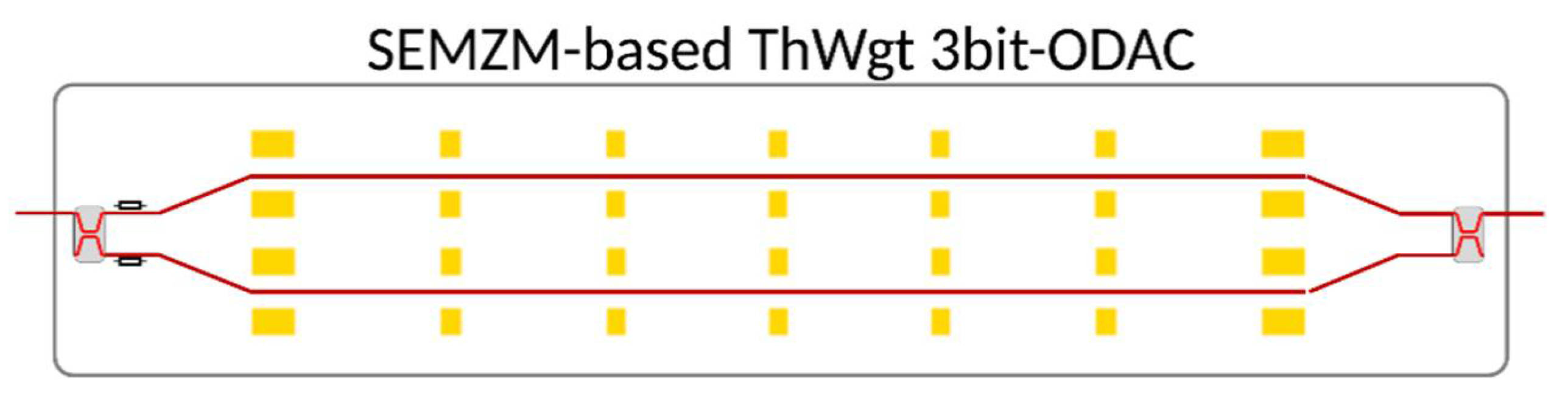
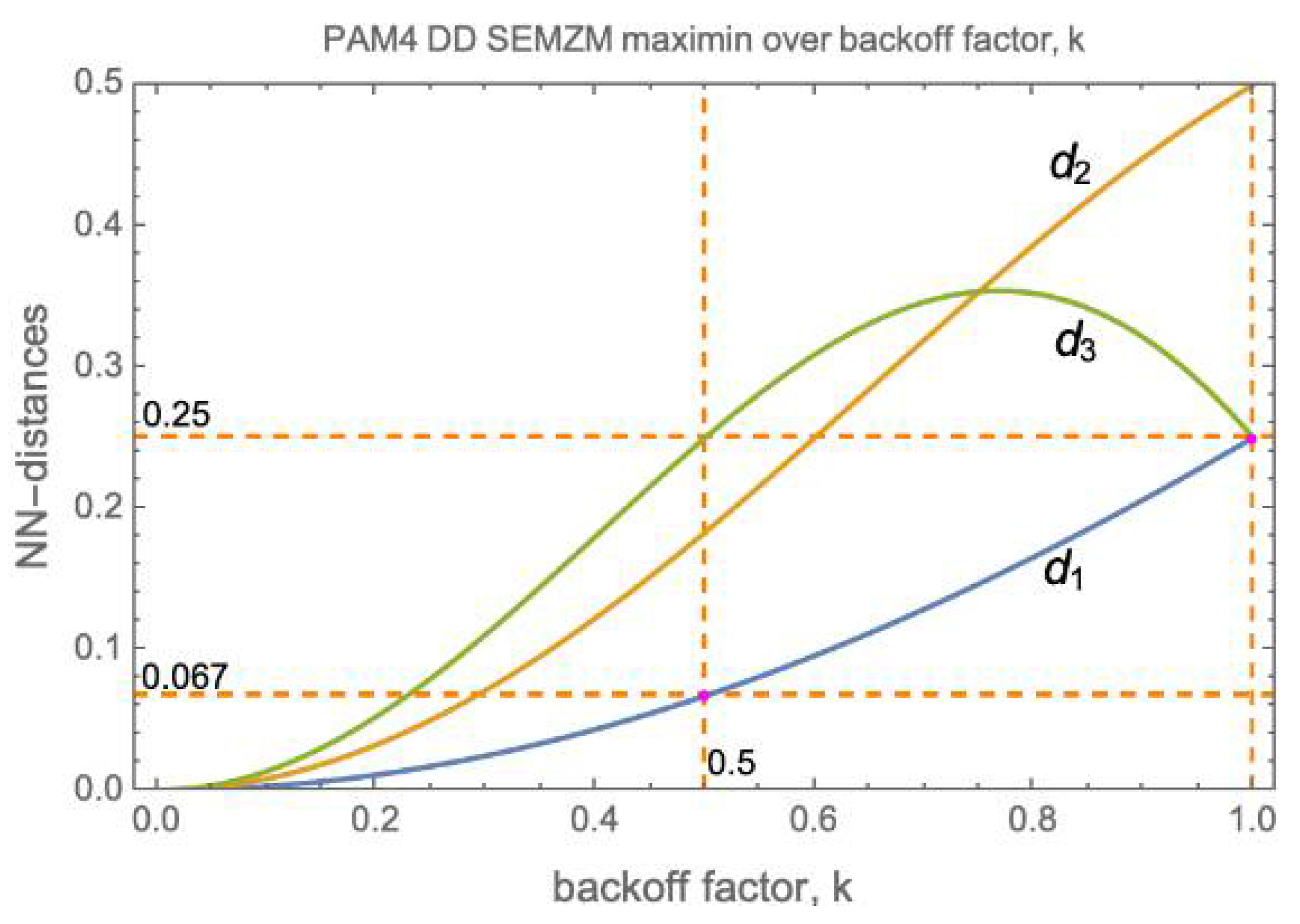
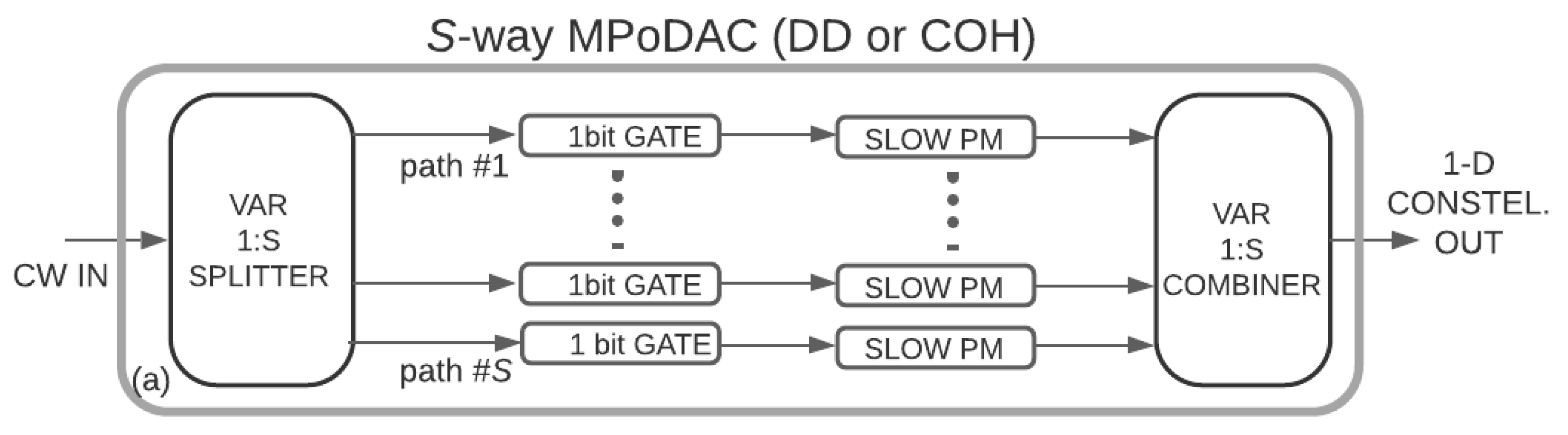
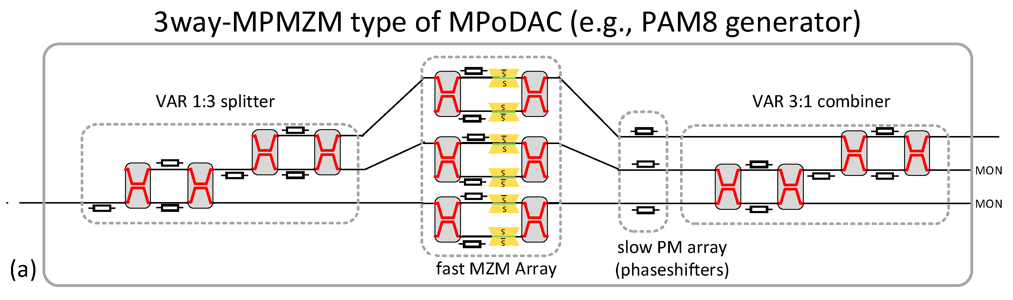
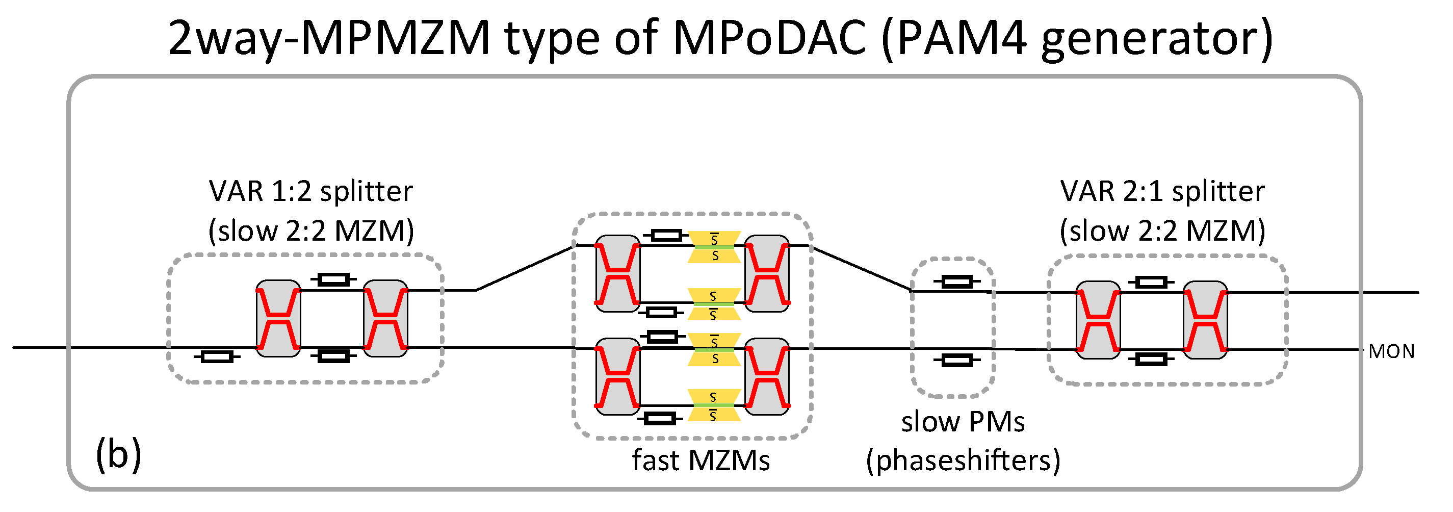
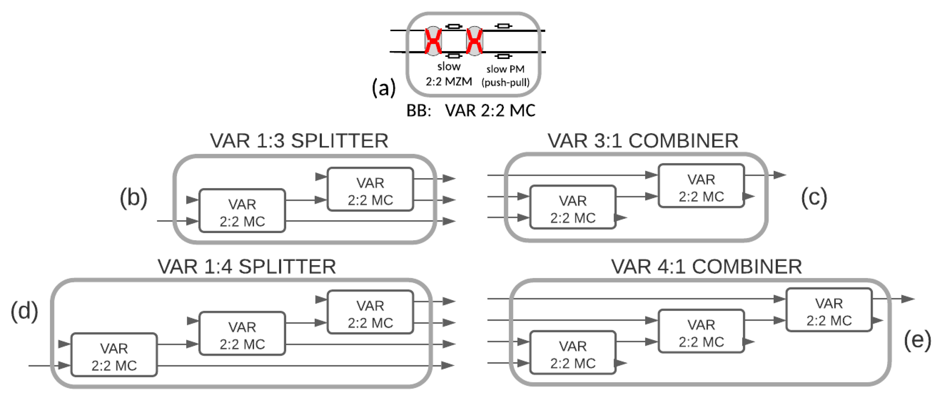
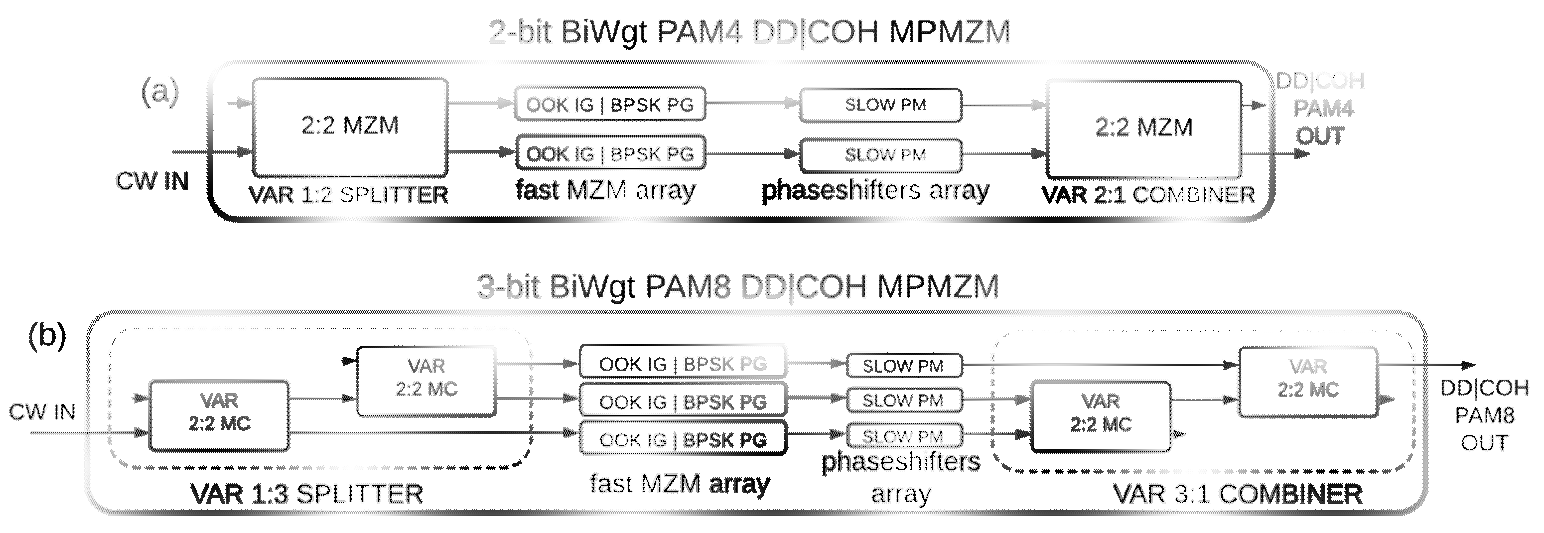
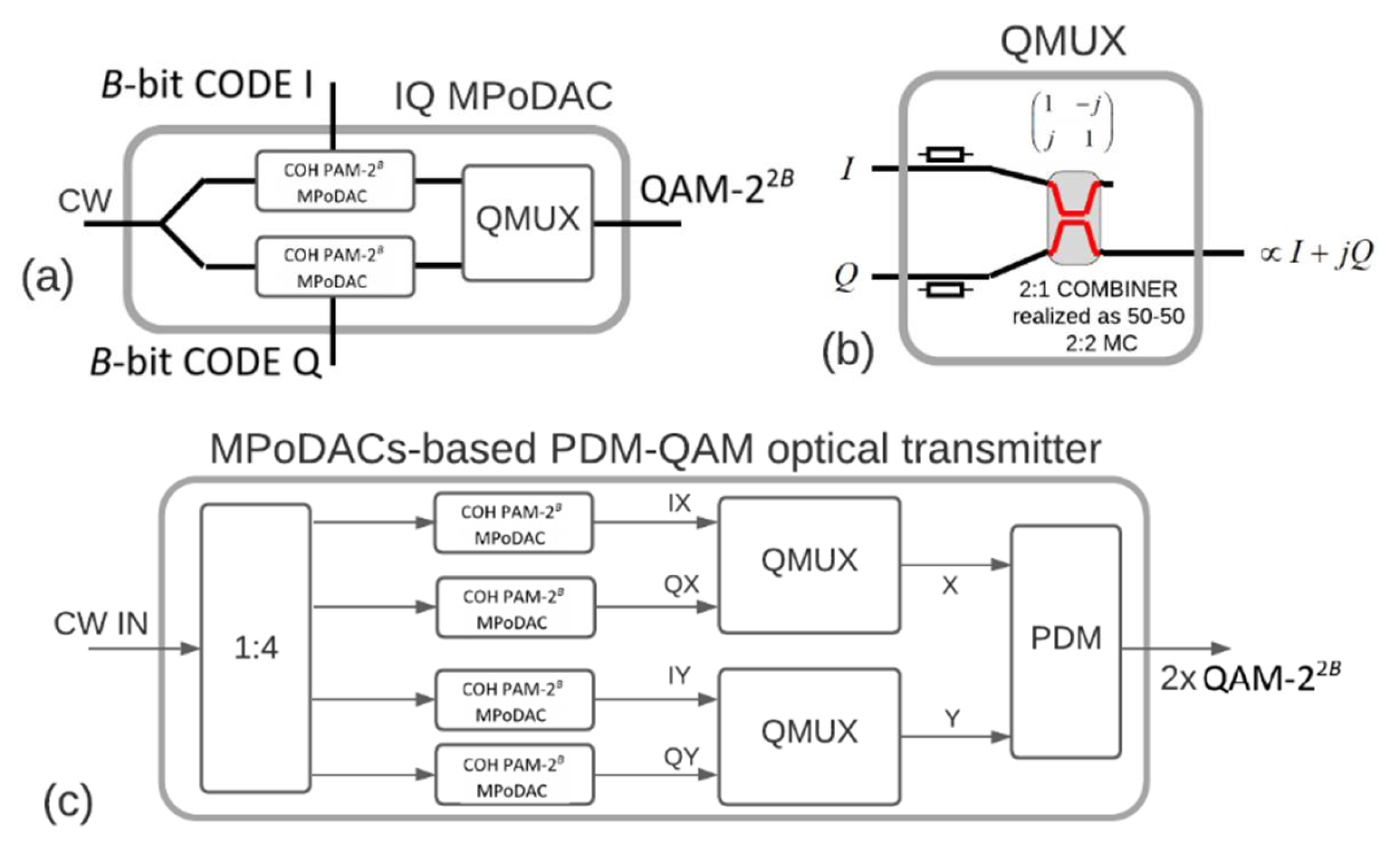
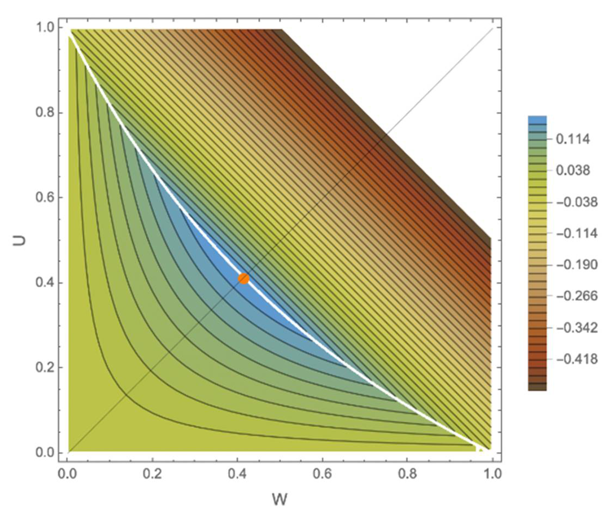
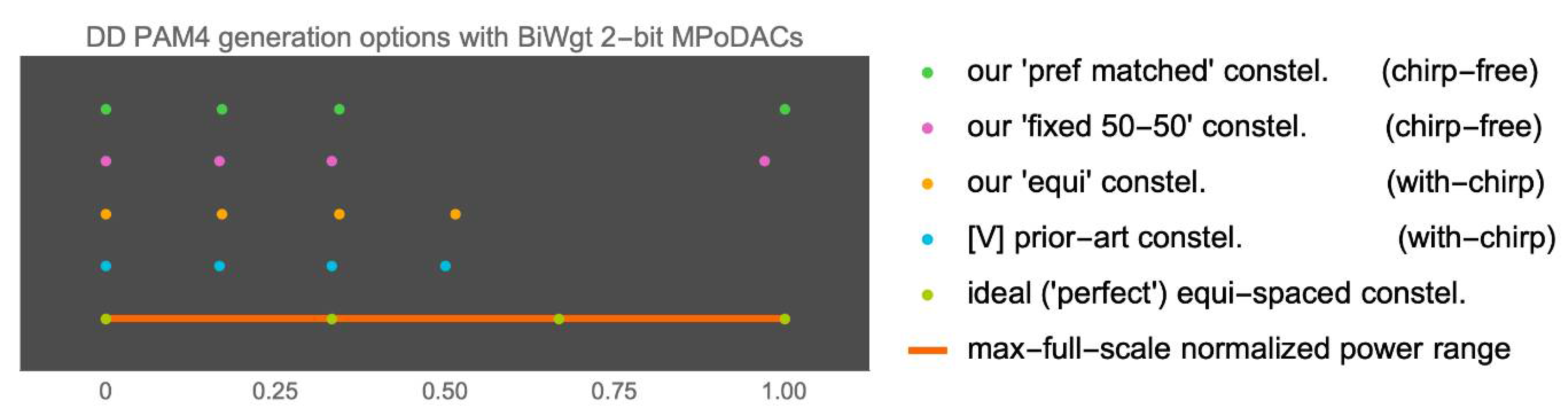
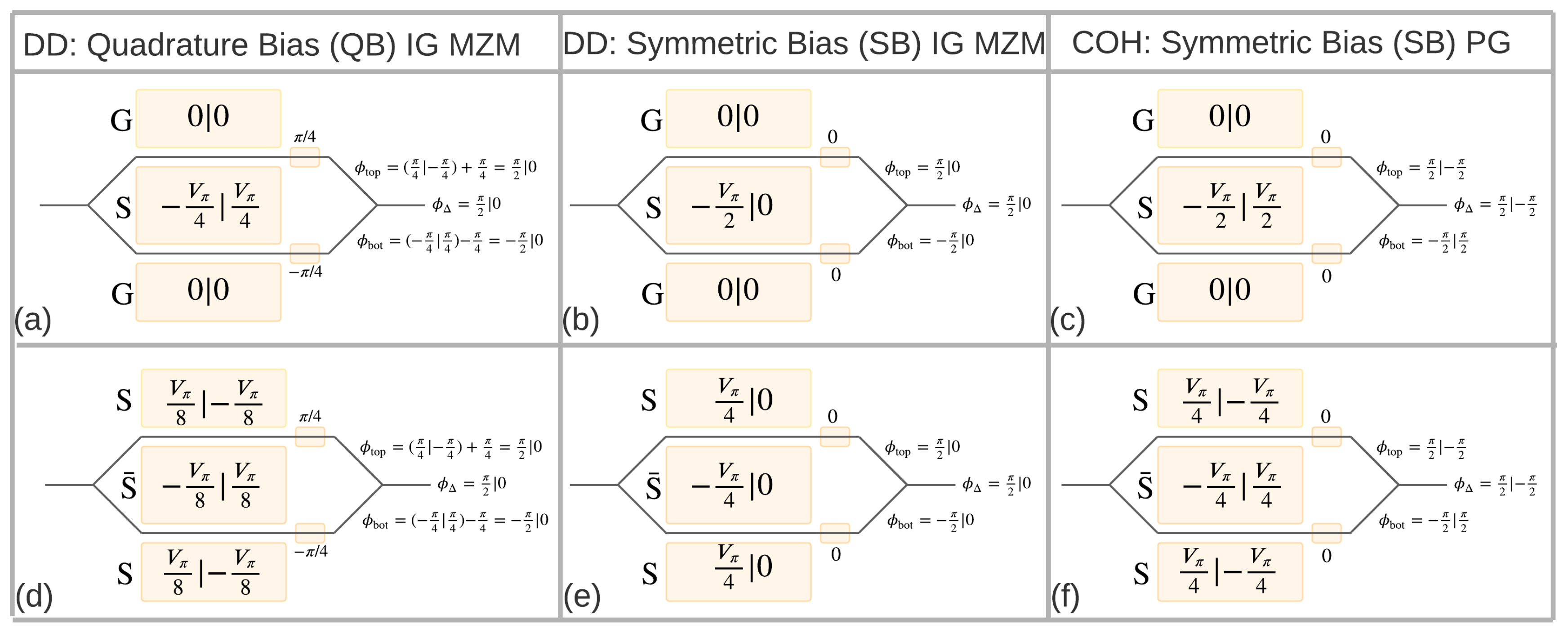
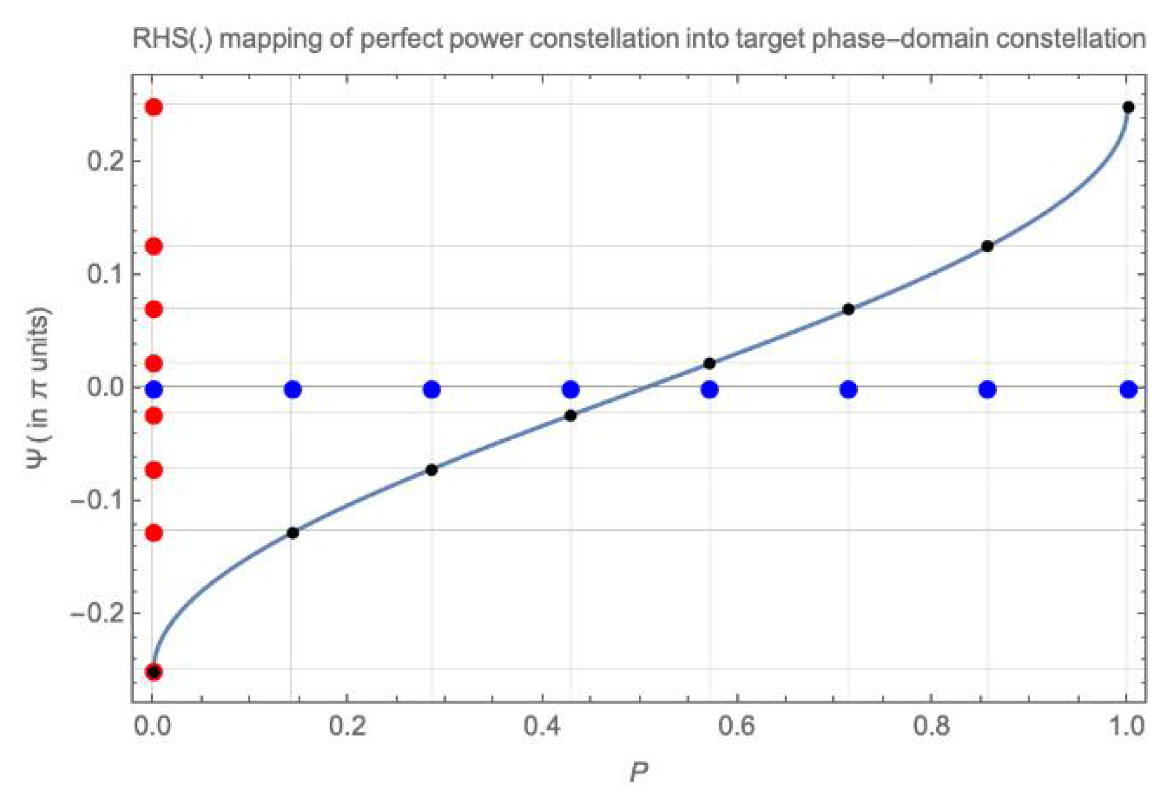


