Article

Proposal of Highly Efficient Quantum Well Microring Resonator-Loaded Optical Phase Modulator Integrated with Antenna-Coupled Electrodes for Radio-over-Fiber

Graduate School of Engineering, Yokohama National University, Yokohama 240-8501, Kanagawa, Japan
*
Author to whom correspondence should be addressed.
Photonics 2021, 8(2), 37; https://doi.org/10.3390/photonics8020037
Submission received: 30 December 2020 / Revised: 26 January 2021 / Accepted: 29 January 2021 / Published: 3 February 2021
(This article belongs to the Special Issue Radio over Fiber)

Abstract

:
Radio-over-fiber (RoF) technology for low-loss, high-speed millimeter-wave transmission using optical fibers has been attracting attention. We propose a highly efficient microring resonator (MRR)-loaded InGaAs/InAlAs multiple-quantum-well (MQW) phase modulator with an antenna coupled electrode (ACE) for 60 GHz RoF systems, and its modulation characteristics are theoretically discussed. This modulator is able to directly convert wireless millimeter-wave (MMW) signals into optical signals without an external power supply. The MRR used in the waveguide structure increases the optical phase change obtained by the unique quantum confinement Stark effect in the MQW through phase enhancement effects, while the ACE based on a coupled microstrip resonant electrode applies a strong standing wave electric field to the waveguide. The proposed modulator is expected to provide tens of times higher phase modulation efficiency than a conventional gap-embedded planar antenna-integrated modulator.

1. Introduction

Wireless millimeter-wave (MMW) technology is a communication method with excellent capacity and high-speed owing to its abundant frequency resources. In particular, the 60 GHz band is allocated internationally as a frequency band that does not require a license [1,2]. IEEE 802.11ay [3] is an ultra-short-range wireless local area network (LAN)standard using the 60 GHz band, which includes new beamforming and channel bonding functions, and is expected to make use of MMW radio for various applications. However, the number of antenna units to construct such wireless MMW systems is enormous, and the signals have relatively high propagation losses due to a large amount of oxygen absorbed in the air. Radio-over-fiber (RoF) technology that offers seamless connections between wireless and optical networks has been investigated [4,5,6,7]. In RoF technology, an RF signal received by an antenna is converted into a lightwave signal by an electro-optic (EO) modulator and transmitted over a low propagation loss silica fiber. This transmission method has a higher usable bandwidth as well as lower loss compared to coaxial cable transmissions. In addition, its high robustness to ambient noise makes it advantageous for the long-distance transmission of wireless MWW signals. Recently, an RoF transmission of 60 GHz radio signals at 31.4 Gbps using orthogonal frequency-division multiplexing (OFDM) has been demonstrated [8]. In conventional RoF systems, MMW signals received by an external antenna are transmitted through coaxial cables and input to an optical modulator. However, it has been pointed out that distortions and delays in MMW signals occur in coaxial cables, and the MMW speed is decreased. Therefore, an antenna-integrated optical modulator is attracting much attention as a new modulation device.
The antenna-integrated modulator is driven directly by received RF signals without an external power supply. Therefore, it has a high affinity that enables low latency communication. The antenna-coupled optical modulator can be applied to the fronthaul of wireless LAN, 5G, and beyond-5G systems [9]. The antenna-coupled optical modulator converts the wireless RF signals from user terminals received at a wireless LAN access point or a remote access point (RAU) to lightwave signals, which are then transmitted to a base station (BS) through optical silica fibers. An approach to building a high-capacity and low-latency RoF system is proposed by installing several dedicated antenna-coupled modulators in a high-density user environment. Furthermore, it is of interest in many applications such as high-resolution radar for airport runways, high-speed rail communication systems, high-precision antenna measurements, and imaging and sensing systems for security applications [10]. There have been reports on antenna-integrated optical modulators based on the Pockels effect of EO materials such as lithium niobate (LN) [10,11,12] and nonlinear optical polymers (EOP) [13,14,15,16]. However, there are some issues such as a relatively small change in refractive index induced by an electric field, large power consumption, poor integration with semiconductor light-emitting devices such as laser diodes (LDs), and enlargement and high losses of an entire system. To date, we reported a printed dipole antenna integrated phase modulator [17,18] with a multiple five-layer asymmetric coupled quantum well (FACQW) [19]. Its high-speed modulation under irradiation of MMW signals is experimentally demonstrated.
In this paper, we propose an InGaAs/InAlAs FACQW microring resonator (MRR)-loaded optical modulator [20,21] integrated with antenna-coupled electrodes (ACE) [22] for the 60 GHz RoF systems, and its modulation characteristics are theoretically discussed. This modulator is able to directly convert wireless MMW signals into optical signals without an external power supply. The electric-field-induced optical phase shift in the MRR waveguide is increased by the unique quantum confinement Stark effect (QCSE) in the FACQW and an enhanced phase shift in the MRR, while the ACE based on a coupled microstrip resonant electrode applies a strong standing wave electric field to the waveguide. Owing to the combination of these effects, the proposed modulator is expected to provide tens of times higher phase modulation efficiency than the previously reported gap-embedded planar antenna-integrated modulator [17].

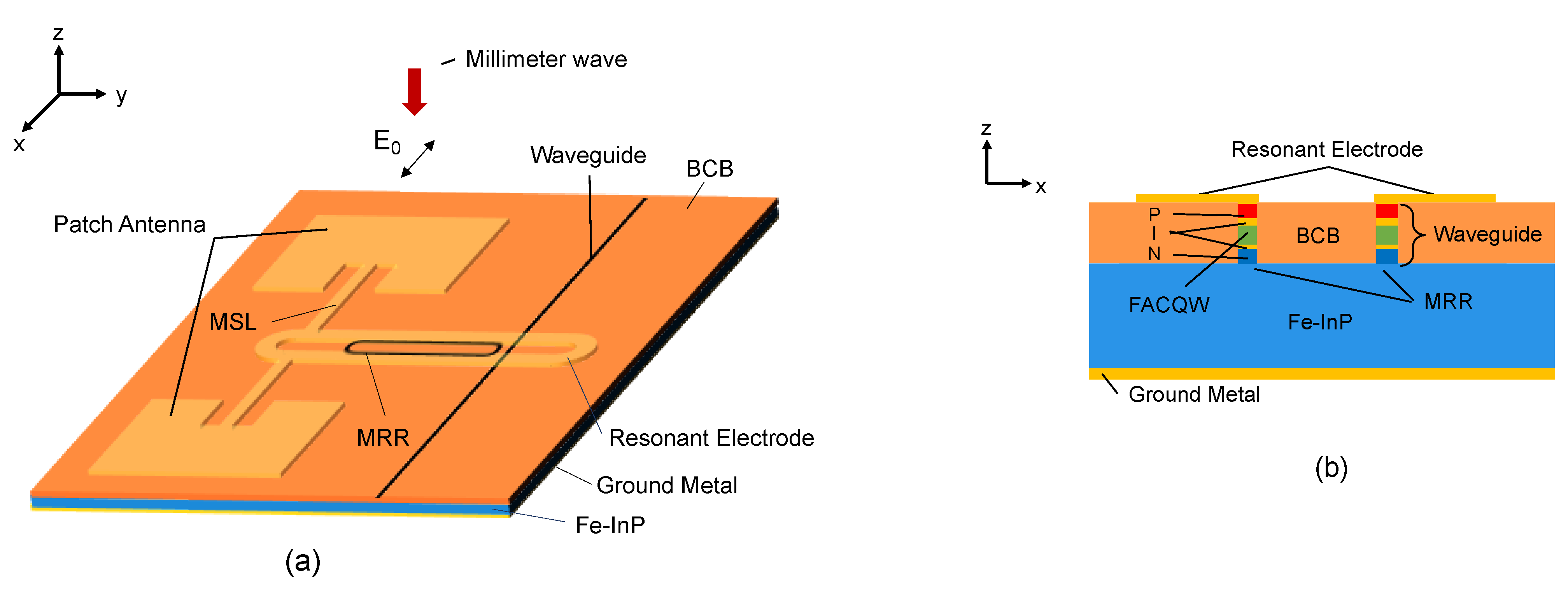
2. Device Design and Operation Principle
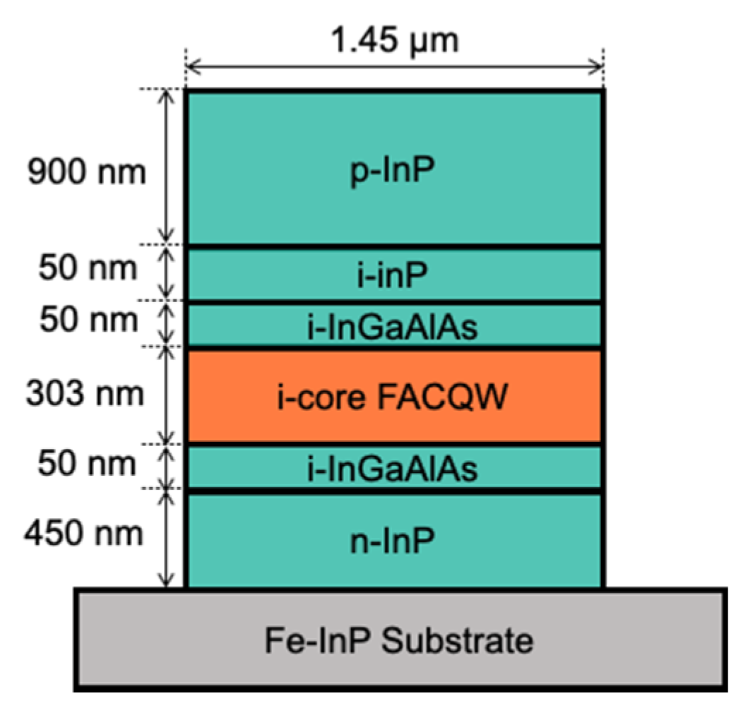
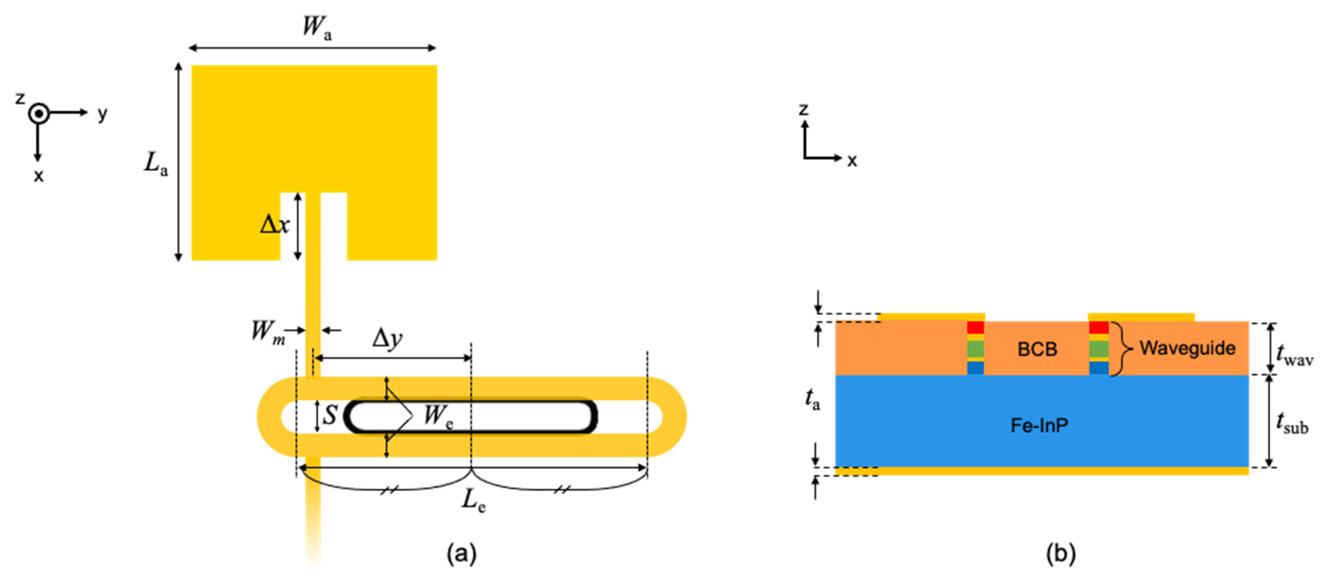
2.1. Device Design

Figure 1 shows a schematic of the proposed phase modulator, which employs Fe-doped InP (Fe-InP) as a substrate to improve the ACE antenna characteristics; the straight part of the MRR waveguide is located along the edge on the gap side of the ACE to efficiently receive voltage signals enhanced as the odd mode.

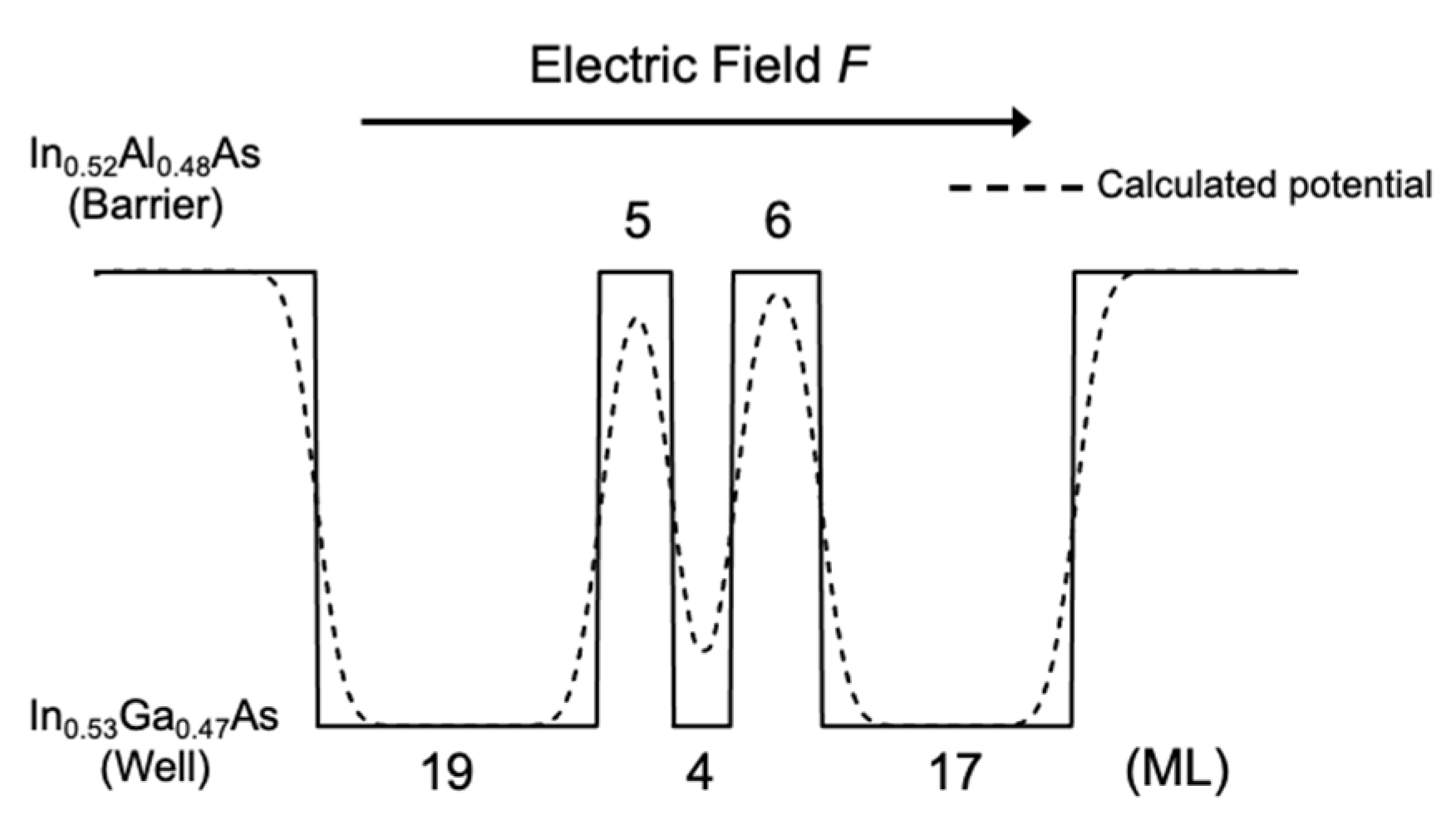
2.1.1. Large Electrorefractive Index Change in InGaAs/InAlAs FACQW

Figure 2 shows the potential diagram of the InGaAs/InAlAs FACQW [18,19], which is used for a core layer of the waveguide in this modulator. Each layer is lattice-matched to InP. The modulator is designed so that the absorption loss is small for the operation wavelength of 1550 nm [17].
Figure 3 shows the calculated electrorefractive index change in the InGaAs/InAlAs FACQW as a function of the electric field for the transverse electric (TE) mode at the wavelength of 1550 nm. The FACQW shows a large differential refractive index change |ΔnF| of approximately 4.0 × 10⁻⁴ cm/kV in the operating range of the reverse electric field F = −8 to −16 kV/cm.
Figure 4 shows a schematic cross-section of the waveguide for the MRR. The waveguide consists of a core layer with 12 sets of InGaAs/InAlAs FACQWs, a 50 nm InAlGaAs separate-confinement heterostructure layer, and p/n-doped InP cladding layers. The doping densities of the upper p-type InP (p-InP) and lower n-type InP (n-InP) cladding layers are assumed to be 1.0 × 1018 cm−3 and 2.0 × 1018 cm−3, respectively. Both sides of the waveguide are buried by benzocyclobutene (BCB), which is a low-refractive-index material. The total thickness of the core layer is approximately 300 nm. The pin diode structure provides a bias electric field of −11.6 kV/cm caused by the built-in potential in the pin junction, which enables the push–pull operation in the operating electric field region of the FACQW. A 50-nm thick undoped InP layer is inserted on top of the core layer to prevent the diffusion of dopants from the p-doped cladding layer and adjust the bias electric field.

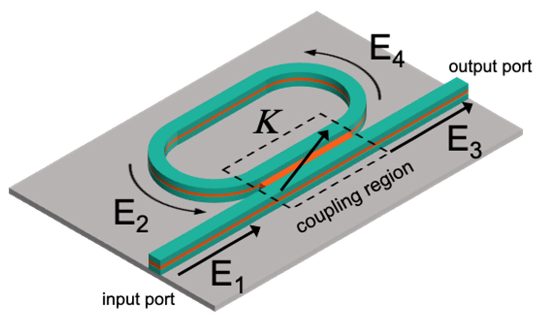
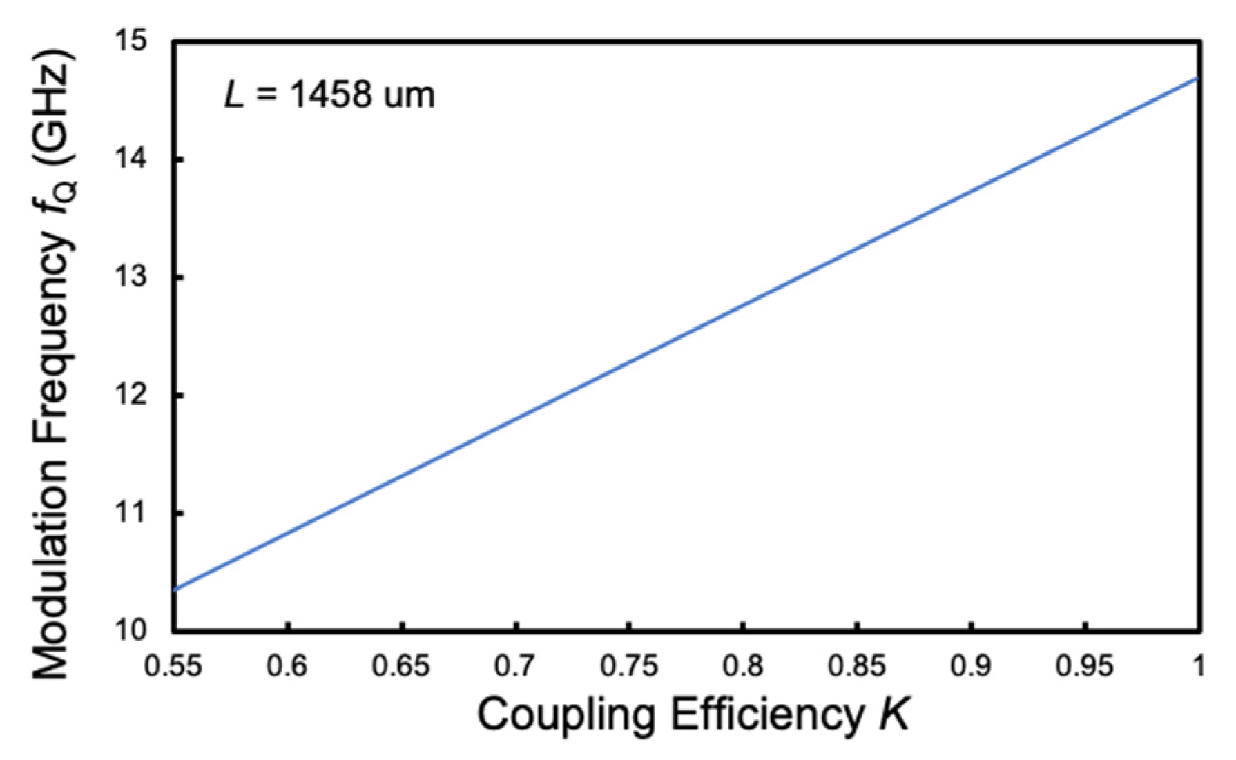
2.1.2. Microring Resonator

A typical ring resonator is a looped optical waveguide, and resonance occurs when the optical path length of the resonator is an integer multiple of the wavelength. In this study, we use the enhanced phase change in an MRR. [20,21] The transmittance of an electric field, T, in the busline waveguide shown in Figure 5 is given by
T = | E 3 E 1 | = | a 2 + r 2 2 a r cos ϕ a 2 r 2 + 1 2 a r cos ϕ | ,
where
r = 1 K ,
a = exp ( α L 2 ) .
The symbol r represents the field transmission coefficient at a coupler between the microring resonator and the busline waveguides. K is the power coupling efficiency, which is the ratio of the power coupling between the microring resonator and the busline waveguide. L is the round-trip length of the MRR, a is the field transmission coefficient, and α is the absorption coefficient. The effective phase change ϕeff is expressed by
ϕ e f f = arg ( E 3 E 1 ) = π + ϕ + arctan ( r sin ϕ a r cos ϕ ) + arctan ( a r sin ϕ 1 a r cos ϕ ) ,
where ϕ is the single-pass phase in the microring defined as −π < ϕ < +π and the total single-pass phase ϕtotal = ϕ (mod 2π). Figure 6 shows the effective phase shift ϕeff as a function of the single-pass phase shift ϕ for K = 0.55, α = 5 Np cm−1, and L = 1458 μm. The remarkable nonlinearity between the effective phase shift Δϕeff and single-pass phase shift Δϕ is strongly enhanced in the on-resonance state.
The phase enhancement factor, representing the phase enhancement effect, is expressed by [21]
| Δ ϕ e f f Δ ϕ | = π ϕ 2 ϕ 1 .
This equation means that the electric field required for driving is reduced by |Δϕeffϕ|−1 by loading an MRR. From Figure 6b, it is necessary to reduce K in order to increase the phase enhancement factor |Δϕeffϕ| and the Q factor. On the other hand, in order to obtain sufficient optical intensity coupled to the microring resonator, K needs to satisfy the over coupling conditions given by
K 1 a 2 .
Since a is assumed to be 5 Np/cm−1 in the proposed waveguide, K needs to be larger than 0.52 in order to satisfy Equation (6). The operating frequency band f of the modulator is expressed using the Q factor of the MRR as follows [23]:
f Q = c λ 0 Q ,
where c is the velocity of light in a vacuum and λ0 is the operating wavelength of light. The frequency of the signal wave irradiated to the modulator needs be lower than the operating frequency band fQ.

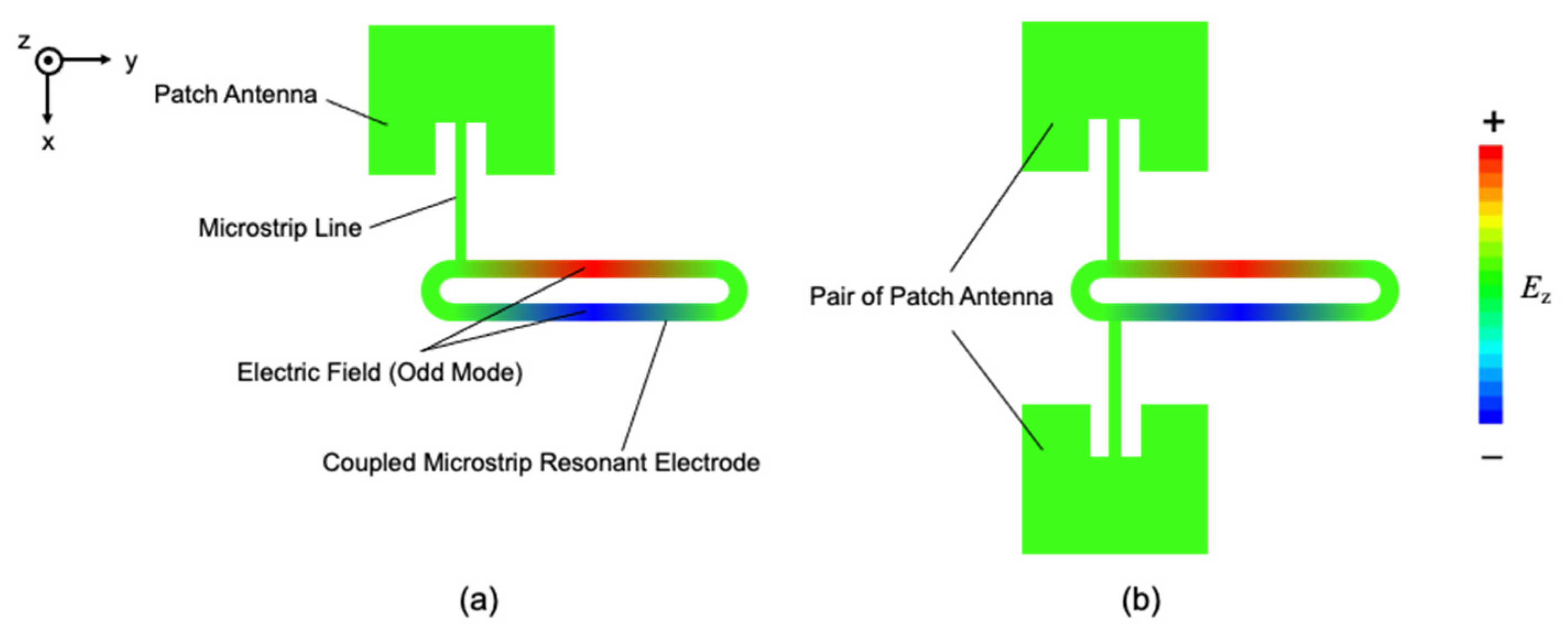
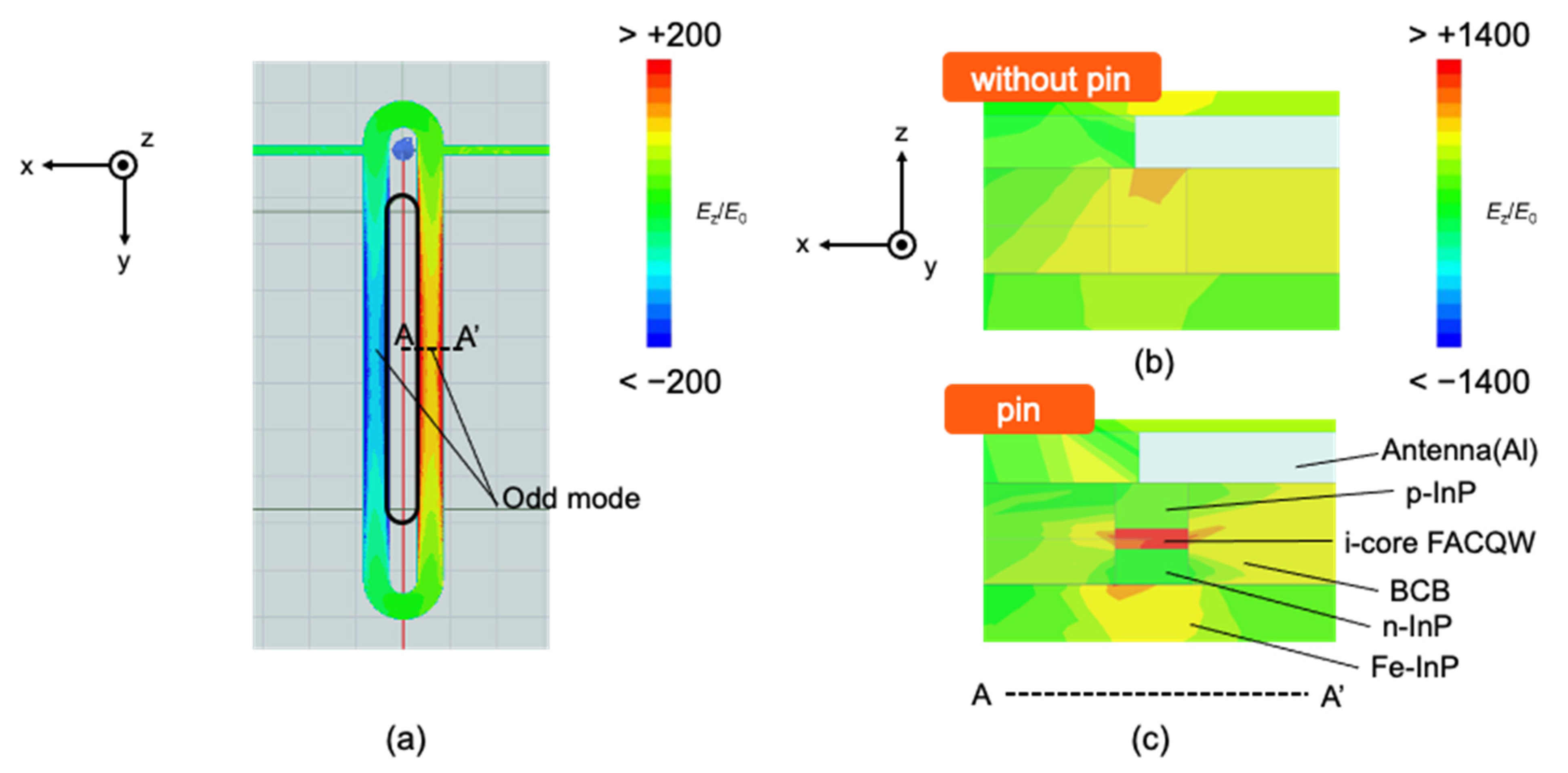
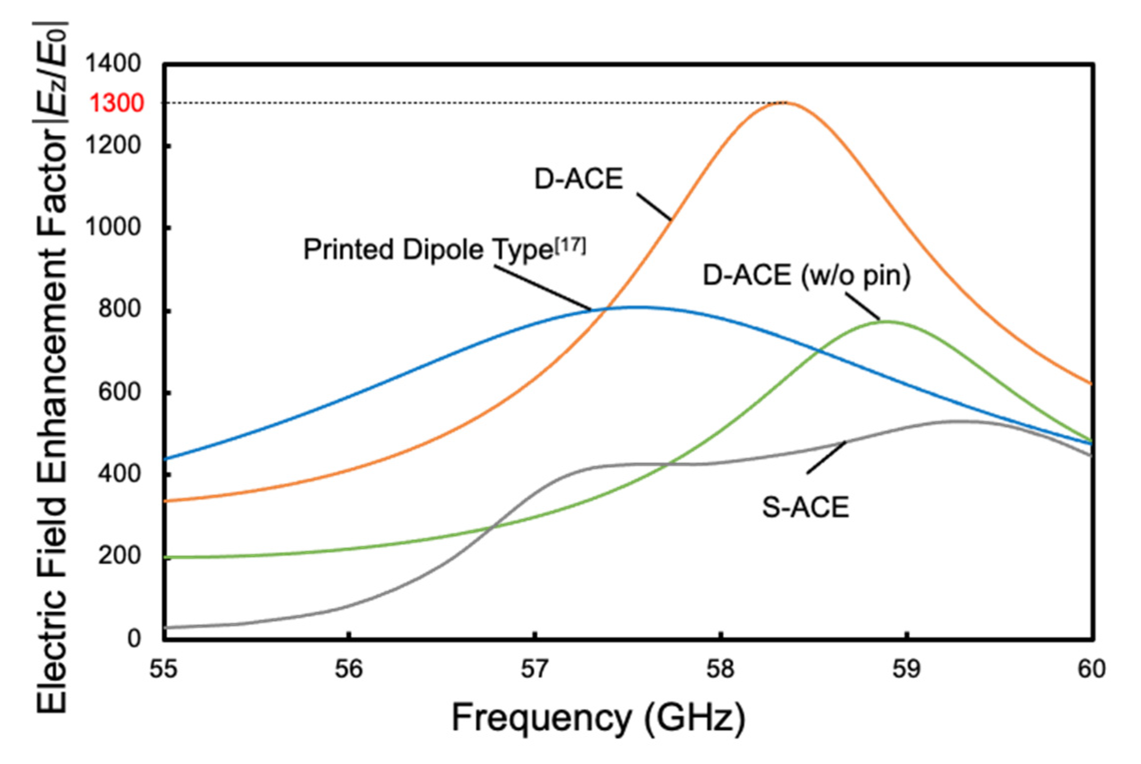
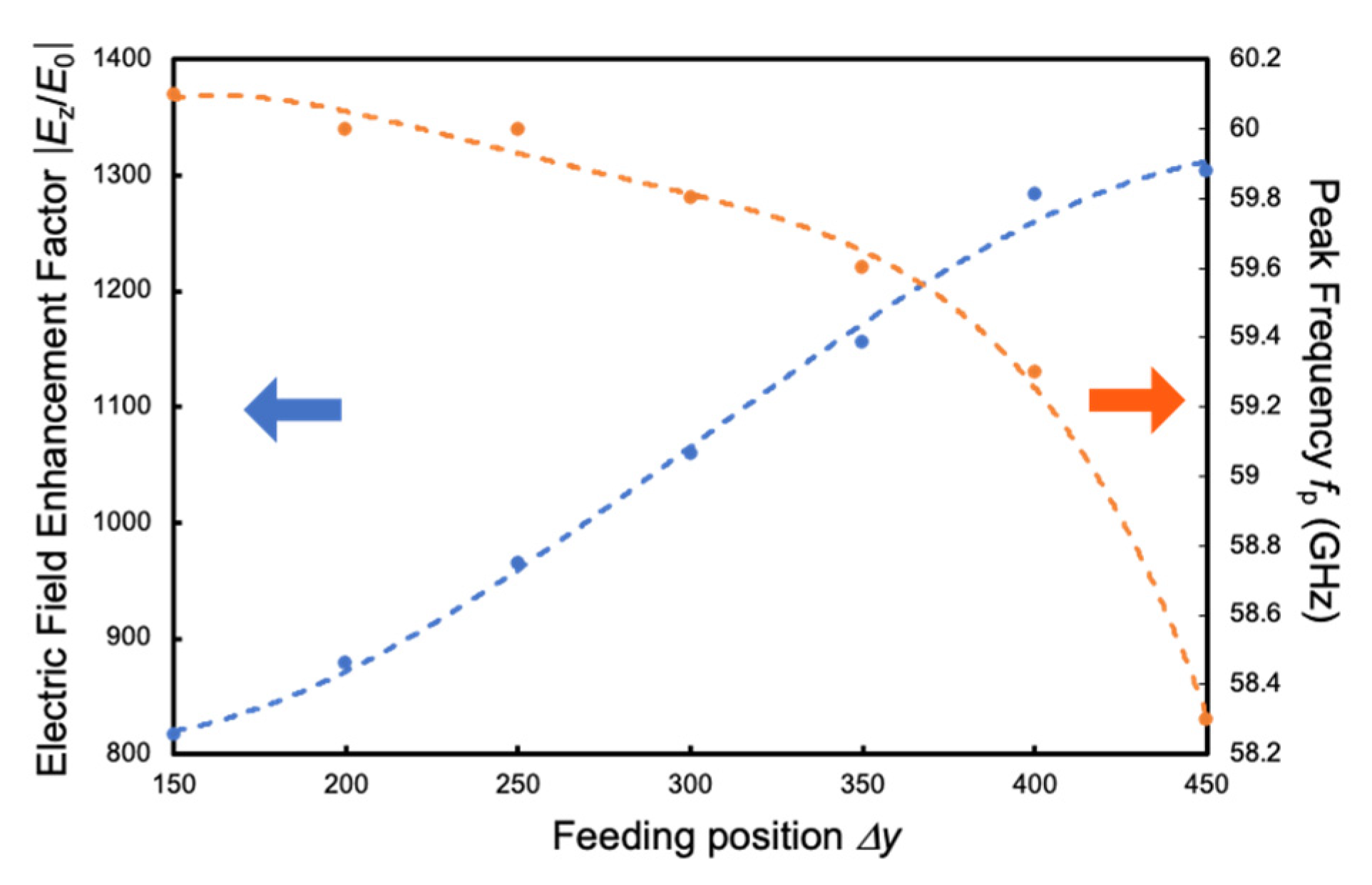
2.1.3. Antenna Coupled Electrode

Figure 7 shows the schematic configuration of the ACE used in the proposed modulator. The ACE consists of a patch antenna and a coupled microstrip resonant electrode. The coupled microstrip resonant electrode consists of a coupled microstrip line (MSL) shorted by a ring-shaped MSL. It generates a standing-wave electric field along the coupled microstrip line by receiving power from the MSL [10]. The coupled MSL also assists in the propagation of odd and even modes [24]. In the case of odd mode, when the potential difference between the ground and the coupled microstrip resonant electrode is V, the potential difference between the two lines of the coupled MSL is 2V. Each mode has a different resonant wavelength, so it is possible to excite the odd mode selectively [25]. By symmetrically coupling double antennas to a coupled microstrip resonant electrode (D-ACE), we can obtain higher efficiency of optical modulation than that of a single antenna resonant electrode (S-ACE). The patch antenna and the resonant electrode are modeled separately in the finite element method (FEM) simulation analysis and designed to minimize the reflection at the fed end. The overall loss due to reflection of the electric field is −18 dB in the D-ACE.

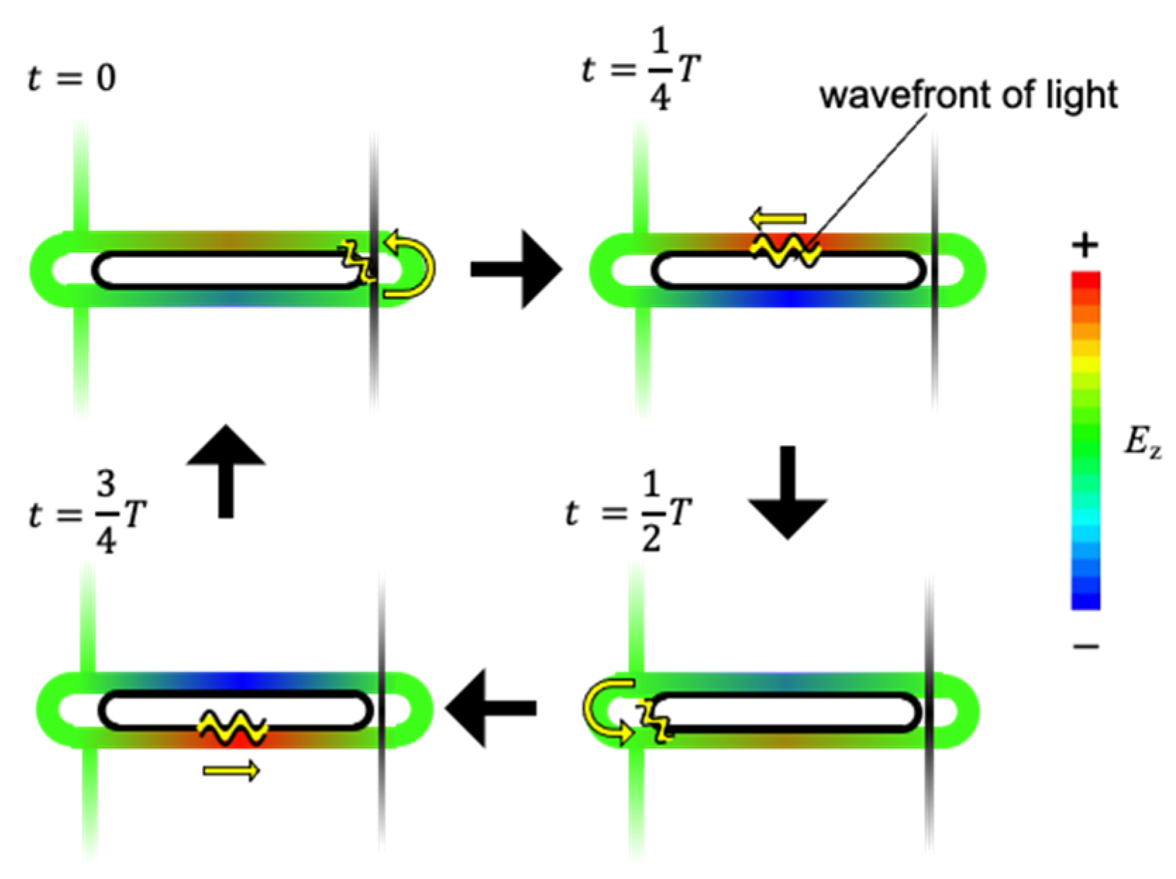
2.2. Operation Principle

Figure 8 explains the relationship between the light propagating in the MRR and the electric field Ez applied to the ring-shaped resonant electrode of the D-ACE. The direction of the electric field caused by the received radio wave changes every half cycle. Therefore, the direction of the refractive index change in the waveguide core layer is also reversed every half cycle. Therefore, in this modulator, the round-trip length and configuration of the MRR is designed so that the light transmitted through the waveguide exactly circles the MRR in one cycle of the alternate electric field caused by the received radio wave. As a result, the electric field Ez applied to the waveguide core layer where the wavefront of the light is always propagating in a constant direction, and the direction of the phase change of the light circling the MRR is always constant as well.
When an ACE is irradiated with an MMW with a frequency f in the z-direction, the standing-wave electric field generated at the resonant electrode is given by
E m 0 ( y , t ) = E z sin ( n m k m y ) cos ( ω m t ) ,
where Ez is the amplitude of the electric field, nm is the effective refractive index for the MMW at the modulation electrode, km is the wavenumber of the MMW in a vacuum, y is the distance the lightwave travels along the MRR, and wm is the angular frequency of the MMW signal.
Equation (8) is not suitable for calculating the electric field applied to an optical waveguide because it represents the electric field distribution in a stationary system. By modifying Equation (8), the electric field observed from the wavefront of the lightwave, when the period of the MMW is consistent with the time of the light propagating in the MRR, is expressed as
E ˜ m ( y , i , ϕ ) = E z sin ( n m k m { y + 1 2 ( i 1 ) u 1 + 1 4 u 1 } ) cos ( n g k m y + ϕ ) ,
where
u 1 = λ m n m λ m n g .
λm is the wavelength of the MMW signal, ng is the group refractive index of the lightwave, ϕ corresponds to the phase of the MMW signal when the lightwave is coupled to the MRR, and i is the number of times the light circulates halfway through the MRR to the other microstrip line side.
However, Equation (9) does not consider the fact that no electric field is applied to the waveguide distributed in the cavity of the resonant electrode. Therefore, the electric field distribution considering the gap is given by
E ˜ M R R ( y , i , ϕ , S ) = { E ˜ m ( y , i , ϕ )   ( π S 2 + ( i 1 ) u 2 y π S 2 + i u 2 ) 0 ( o t h e r w i s e ) ,
where
u 2 = λ R F 2 n g ,
and S is the electrode separation. From the above results, the phase change of the lightwave propagating the MRR can be expressed as
D = π λ o p n e f f r F A C Q W Γ L M R R × 0 2 N u 2 E ˜ M R R ( y , i , ϕ , S ) d y 2 N u 2 ,
where λop is the wavelength of the light, neff is the effective refractive index of the core layer, rFACQW is the coefficient of refractive index change in the FACQW, i.e., |ΔnF|, and Γ is the overlap coefficient between the Ez applied to the core layer and the optical electric field of the lightwave propagating in the FACQW core layer, and LMRR is the round-trip length of the MRR, and N is the number of times the lightwave travels around the MRR. Since Equation (13) represents the phase change per revolution of light in the MRR, the cumulative phase change in the MRR can be calculated with Equations (4) and (13).

3. Result and Discussion

3.1. MMW Characteristics

Figure 9 shows the schematic view of each parameter of the proposed modulator, and Table 1 shows the numerical values of each parameter obtained by the analysis. The parameters of the ACE were designed with reference to [26,27]. The coupling efficiency K satisfies the over coupling condition K 1 − a2 ~ 0.52. The MMW characteristics of the proposed modulators were analyzed using the FEM, and the MMW analysis was performed by irradiating the plane wave signals of the x-polarized light in the 60 GHz band.
Figure 10 shows the electric field enhancement factor Ez/E0 below the antenna when the antenna is irradiated with a y-polarized 60 GHz plane wave. As shown in Figure 10a, the odd mode is excited where the electric field is induced in both positive and negative directions along the resonant electrode. The electric field Ez around the inner edge is larger than that in the middle of the MSL of the resonant electrode, which means that the electric field is efficiently applied to the optical waveguide. Figure 10b shows the electric field enhancement factor Ez/E0 in the cross-section of the waveguide with and without the pin junction. In the pin junction, the electric field is concentrated in the nondoped layer (i-layer) composed of the FACQW, and a larger electric field is induced.
Figure 11 shows the electric field enhancement factor |Ez/E0| calculated as a function of the frequency of the MMW. Ez was calculated as the maximum value from the electric field applied to the core layer. The peak frequency fp of the D-ACE was calculated to be 58.3 GHz. At the peak frequency, |Ez/E0| is evaluated to be 1300, which means that the electric field applied to the core layer, Ez, is increased by 1300 times of the incident MMW magnitude E0.
On the other hand, maximum |Ez/E0| is 780 in the structure without the pin junction. This indicates that Ez is enhanced by 1.7 times by using the pin junction. In the case of S-ACE, at the peak frequency, |Ez/E0| of 530 of the incident MMW magnitude E0 can be applied to the core layer. This value indicates that the electric field enhancement in the D-ACE is approximately 2.5 times larger than that in the S-ACE. This is attributed to the fact that the D-ACE has twice the antenna aperture area of the S-ACE, and the MSLs are symmetrically coupled to the coupled microstrip resonant electrode, resulting in less distortion of the standing wave field. The small peak observed at 57.2 GHz in the S-ACE curve is caused by the resonance of the electric field in the MSL between the antenna and the junction of the microstrip antenna (MSA) and the resonant electrode. On the other hand, such a peak is not observed in the D-ACE curve because the impedance of the resonant electrode is changed by the MSL on the other side, and the resonance at 57.2 GHz is suppressed. Compared with the previously reported printed dipole type device with a pin junction [17], the D-ACE is approximately 1.63 times as large as |Ez/E0|.
Figure 12 shows the relationship between the electric field enhancement factor |Ez/E0| and the distance Δy from the center of the coupled microstrip resonant electrode to the feeding point of the MSL. We can see that |Ez/E0| increases with the increase in Δy, and the peak frequency shifts to the high-frequency side. This is due to the fact that the characteristic impedance is higher when Δy is smaller because the standing wave field induced in the coupled microstrip resonant electrode has its peak near the center. In this modulator, the MSL, MSA, and a coupled microstrip resonant electrode are impedance-matched at 110 Ω, which is much smaller than the characteristic impedance at Δy = 0. Therefore impedance matching is easier for smaller Δy.
Figure 13 shows the relationship between the electric field enhancement factor |Ez/E0| and the frequency, where the effect of the phase mismatch between the electric field applied to the MRR waveguide and the light propagating in the MRR is considered in addition to the frequency response of the ACEs obtained in Figure 11. The number of times the light circulates in the MRR, F, is assumed to be 2.5 (i = 4). Here, the finesse of an MRR, F, is given by [23]
F = π r a 1 r a .
The finesse represents the number of times the light travels around the MRR before its energy is reduced to 1/e of the incident light power. Although the 3 dB bandwidth of the D-ACE is narrower than that of the printed dipole antenna type modulator, it is still as wide as 1.6 GHz. The 3 dB bandwidth of the S-ACE is approximately two times as wide as that of the D-ACE due to the influence of the small peak observed in Figure 11.

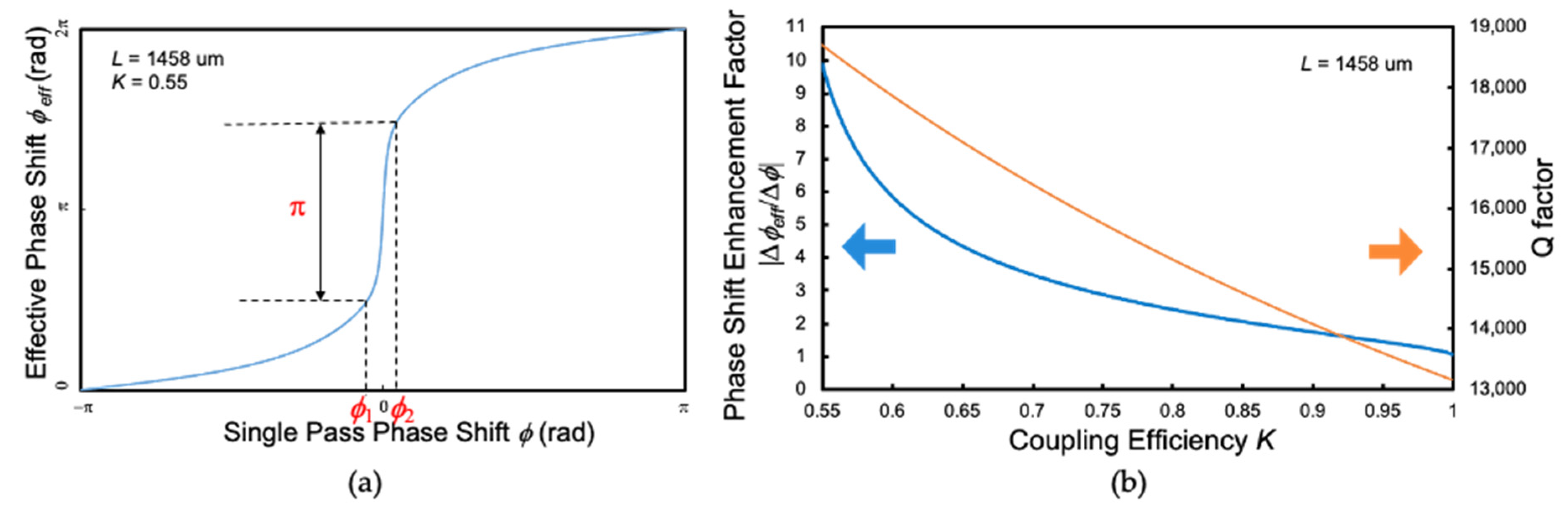
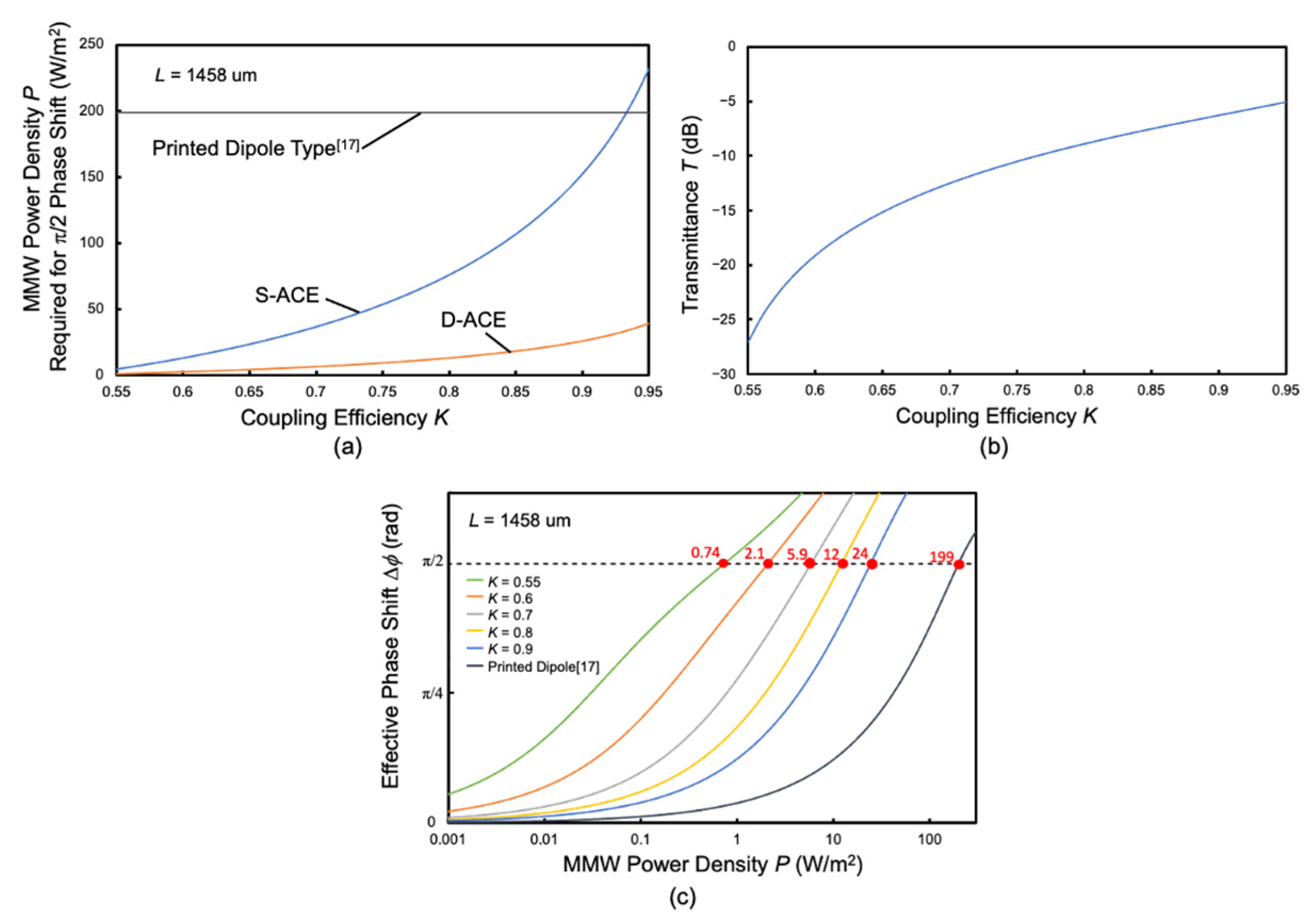
3.2. Phase Modulation Characteristics

Figure 14 shows the relationship between the coupling efficiency K, phase change f, and transmittance T. The phase change was calculated by substituting the electric field enhancement factor |Ez/E0| at the peak frequency obtained from Figure 11 into Ez in Equation (14). In Figure 14a, we can see that the input power density required for driving, P, decreases with the decrease in the coupling efficiency K. On the other hand, Figure 14b shows that the transmittance T also decreases and the insertion loss increases with the decrease in K. That is, there is a trade-off between the phase enhancement effect and the insertion loss. Considering the insertion loss, K of 0.8 or larger is preferable for practical use. In the case of K = 0.8, the input power required to obtain a phase change of π/2 is 12.
W/m2, which means that the modulation efficiency of the D-ACE modulator is 16.6 times higher than that of the printed dipole type modulator.
Figure 15 shows the relationship between the coupling efficiency K and the modulation speed fQ of the MRR. The frequency allocation of the 60 GHz band assumed in this modulator is roughly 57~66 GHz [1]. Therefore, the frequency of the modulated wave is less than 10 GHz at most. This means that this MRR structure has a sufficient modulation bandwidth in the range of coupling efficiency K that satisfies the over coupling condition.
The proposed modulator is expected to exhibit the excellent characteristics discussed in this paper when the device is fabricated as designed. In particular, the electric-field-induced change in the refractive index in the FACQW significantly deteriorates unless each layer is grown according to the designed structure with the accuracy of a few monolayers (ML, 0.293 nm), as discussed in [28]. The relative positions of the resonant electrode and the optical waveguide are also important to obtain the expected electric field enhancement factor. Fabrication errors in the positions are desired to be within 1.0 μm.
The phase modulation of p/2 rad of the proposed modulator (D-ACE) can be obtained with an input power density of 12 W/m2 in the 60 GHz band. Its modulation efficiency is expected to be three orders of magnitude larger than that of an antenna-integrated LN modulator [12] and two orders of magnitude larger than that of an antenna-integrated plasmonic modulator [13]. On the other hand, the 3 dB bandwidth of the D-ACE modulator is 1.6 GHz, which is approximately half of those of the LN and plasmonic modulators.

4. Conclusions

We proposed the InGaAs/InAlAs FACQW phase modulator composed of a coupled microstrip resonant electrode and MRR, and its RF and modulation characteristics were theoretically discussed. Owing to the strong resonant electric field by the coupled microstrip resonant electrode, the field intensity enhancement rate for the core layer is approximately 1.63 times higher than that of the printed dipole modulator. By utilizing both the large enhancement of the electric field in the resonant electrode and the large phase shift enhancement effect in the MRR, the phase change of tens of times higher than that of a printed dipole antenna-integrated modulator is expected to be obtained.

Author Contributions

Conceptualization, H.K. and T.A.; methodology, H.K. and T.A.; design and simulation, H.K.; writing—original draft preparation, H.K.; writing—review and editing, H.K. and T.A.; supervision, T.A. All authors have read and agreed to the published version of the manuscript.

Funding

This research was partly funded by a Grant-in-Aid for Scientific Research B (No. 18H01897) from the Ministry of Education, Culture, Sports, Science and Technology, Japan.

Acknowledgments

The authors express sincere thanks to Joo-Hyong Noh at Kanto Gakuin University for supporting electromagnetic analysis using the FEM simulator.

Conflicts of Interest

The authors declare no conflict of interest.

References

  1. Koji, T.; Naganori, S.; Kazuaki, T. 60 GHz band wireless access technology based on IEEE 802.11ad/WiGig and its future perspectives. IEICE Tech. Rep. 2017, 116, 207–212. [Google Scholar]
  2. Singh, H.; Prasad, R.; Bonev, B. The Studies of Millimeter Waves at 60 GHz in Outdoor Environments for IMT Applications: A State of Art. Wirel. Pers. Commun. 2018, 100, 463–474. [Google Scholar] [CrossRef] [Green Version]
  3. Ghasempour, Y.; da Silva, C.R.C.M.; Cordeiro, C.; Knightly, E.W. IEEE 802.11ay: Next-Generation 60 GHz Communication for 100 Gb/s Wi-Fi. IEEE Commun. Mag. 2017, 55, 186–192. [Google Scholar] [CrossRef]
  4. Beas, J.; Castanon, G.; Aldaya, I.; Aragon-Zavala, A.; Campuzano, G. Millimeter-Wave Frequency Radio over Fiber Systems: A Survey. IEEE Commun. Surv. Tutor. 2013, 15, 1593–1619. [Google Scholar] [CrossRef]
  5. Capmany, J.; Novak, D. Microwave Photonics Combines Two Worlds. Nat. Photonics 2007, 1, 319–330. [Google Scholar] [CrossRef]
  6. Marti, J.; Capmany, J. Microwave Photonics and Radio-over-Fiber Research. IEEE Microw. Mag. 2009, 10, 96–105. [Google Scholar] [CrossRef]
  7. Seeds, A.J.; Williams, K.J. Microwave Photonics. J. Lightwave Technol. 2006, 24, 4628–4641. [Google Scholar] [CrossRef]
  8. Ng’oma, A.; Lin, C.; He, L.Y.W.; Jiang, W.; Annunziata, F.; Chen, J.; Shih, P.; George, J.; Chi, S. 31 Gbps RoF System Employing Adaptive Bit-Loading OFDM Modulation at 60 GHz. In Proceedings of the 2011 Optical Fiber Communication Conference and Exposition and the National Fiber Optic Engineers Conference, Los Angeles, CA, USA, 6–10 March 2011; pp. 1–3. [Google Scholar]
  9. Cao, Z.; Ma, Q.; Smolders, A.B.; Jiao, Y.; Wale, M.J.; Oh, C.W.; Wu, H.; Koonen, A.M.J. Advanced Integration Techniques on Broadband Millimeter-Wave Beam Steering for 5G Wireless Networks and Beyond. IEEE J. Quantum Electron. 2016, 52, 1–20. [Google Scholar] [CrossRef]
  10. Murata, H. Millimeter-Wave-Band Electro-Optic Modulators Using Antenna-Coupled Electrodes for Microwave Photonic Applications. J. Lightwave Technol. 2020, 38, 5485–5491. [Google Scholar] [CrossRef]
  11. Sheehy, F.T.; Bridges, W.B.; Schaffner, J.H. 60 GHz and 94 GHz Antenna-Coupled LiNbO3 Electrooptic Modulators. IEEE Photonics Technol. Lett. 1993, 5, 307–310. [Google Scholar] [CrossRef]
  12. Wijayanto, Y.N.; Murata, H.; Okamura, Y. Electrooptic Millimeter-Wave–Lightwave Signal Converters Suspended to Gap-Embedded Patch Antennas on Low-k Dielectric Materials. IEEE J. Sel. Top. Quantum Electron. 2013, 19, 33–41. [Google Scholar] [CrossRef]
  13. Salamin, Y.; Baeuerle, B.; Heni, W.; Abrecht, F.C.; Josten, A.; Fedoryshyn, Y.; Haffner, C.; Bonjour, R.; Watanabe, T.; Burla, M.; et al. Microwave Plasmonic Mixer in a Transparent Fibre–Wireless Link. Nat. Photonics 2018, 12, 749–753. [Google Scholar] [CrossRef] [PubMed]
  14. Herrera, O.D.; Kim, K.; Voorakaranam, R.; Himmelhuber, R.; Wang, S.; Demir, V.; Zhan, Q.; Li, L.; Norwood, R.A.; Nelson, R.L.; et al. Silica/Electro-Optic Polymer Optical Modulator with Integrated Antenna for Microwave Receiving. J. Lightwave Technol. 2014, 32, 3861–3867. [Google Scholar] [CrossRef]
  15. Zhang, X.; Hosseini, A.; Subbaraman, H.; Wang, S.; Zhan, Q.; Luo, J.; Jen, A.K.-; Chen, R.T. Integrated Photonic Electromagnetic Field Sensor Based on Broadband Bowtie Antenna Coupled Silicon Organic Hybrid Modulator. J. Lightwave Technol. 2014, 32, 3774–3784. [Google Scholar] [CrossRef]
  16. Park, D.H.; Pagán, V.R.; Murphy, T.E.; Luo, J.; Jen, A.K.-Y.; Herman, W.N. Free Space Millimeter Wave-Coupled Electro-Optic High Speed Nonlinear Polymer Phase Modulator with in-Plane Slotted Patch Antennas. Opt. Express 2015, 23, 9464–9476. [Google Scholar] [CrossRef] [Green Version]
  17. Miyazeki, Y.; Arakawa, T. Proposal of InGaAs/InAlAs Multiple Quantum Well Mach–Zehnder Modulator Integrated with Array of Planar Antennas. Jpn. J. Appl. Phys. 2019, 58, SJJE05. [Google Scholar] [CrossRef]
  18. Miyazeki, Y.; Yokohashi, H.; Kodama, S.; Murata, H.; Arakawa, T. InGaAs/InAlAs Multiple-Quantum-Well Optical Modulator Integrated with a Planar Antenna for a Millimeter-Wave Radio-over-Fiber System. Opt. Express 2020, 28, 11583–11596. [Google Scholar] [CrossRef]
  19. Arakawa, T.; Toya, T.; Ushigome, M.; Yamaguchi, K.; Ide, T.; Tada, K. InGaAs/InAlAs Five-Layer Asymmetric Coupled Quantum Well Exhibiting Giant Electrorefractive Index Change. Jpn. J. Appl. Phys. 2011, 50, 032204. [Google Scholar] [CrossRef]
  20. Kaneshige, H.; Ueyama, Y.; Yamada, H.; Yajima, H.; Arakawa, T.; Kokubun, Y. InGaAs/InAlAs Multiple Quantum Well Mach–Zehnder Modulator with Single Microring Resonator. Jpn. J. Appl. Phys. 2012, 51, 02BG01. [Google Scholar] [CrossRef]
  21. Kaneshige, H.; Gautam, R.; Ueyama, Y.; Katouf, R.; Arakawa, T.; Kokubun, Y. Low-Voltage Quantum Well Microring-Enhanced Mach-Zehnder Modulator. Opt. Express 2013, 21, 16888–16900. [Google Scholar] [CrossRef]
  22. Murata, H.; Miyanaka, R.; Okamura, Y. Wireless Space-Division-Multiplexed Signal Discrimination Device Using Electro-Optic Modulator with Antenna-Coupled Electrodes and Polarization-Reversed Structures. Int. J. Microw. Wirel. Technol. 2012, 4, 399–405. [Google Scholar] [CrossRef]
  23. Bogaerts, W.; De Heyn, P.; Van Vaerenbergh, T.; De Vos, K.; Kumar Selvaraja, S.; Claes, T.; Dumon, P.; Bienstman, P.; Van Thourhout, D.; Baets, R. Silicon Microring Resonators. Laser Photonics Rev. 2012, 6, 47–73. [Google Scholar] [CrossRef]
  24. Gupta, K.C.; Garg, R.; Bahl, I.J. Microstrip Lines and Slotlines; Artech House: Norwood, MA, USA, 1979. [Google Scholar]
  25. Enokihara, A.; Yajima, H.; Murata, H.; Okamura, Y. Electro-Optic Intensity Modulator Using Higher-Order Resonant Electrode with Polarization-Reversed Structure. In Proceedings of the 2005 European Microwave Conference, Paris, France, 4–6 October 2005. [Google Scholar] [CrossRef]
  26. Kirschning, M.; Jansen, R.H. Accurate Wide-Range Design Equations for the Frequency-Dependent Characteristic of Parallel Coupled Microstrip Lines. IEEE Trans. Microw. Theory Tech. 1984, 32, 83–90. [Google Scholar] [CrossRef]
  27. Enokihara, A.; Yajima, H.; Murata, H.; Okamura, Y. Guided-Wave EO Intensity Modulator Using Coupled Microstrip Line Electrode of Higher-Order Harmonic Resonance Combined with Polarization-Reversed Structure. IEICE Trans. Electron. 2007, E90-C, 1096–1104. [Google Scholar] [CrossRef]
  28. Tada, K.; Arakawa, T.; Kazuma, K.; Kurosawa, N.; Noh, J.H. Influence of One Monolayer Thickness Variation in GaAs/AlGaAs Five-Layer Asymmetric Coupled Quantum Well upon Electrorefractive Index Change. Jpn. J. Appl. Phys. 2001, 40, 656–661. [Google Scholar] [CrossRef]
Figure 1. Schematic view of proposed modulator. (a) Whole view and (b) cross-sectional view in x–z plane.
Photonics 08 00037 g001
Figure 2. Potential profile of InGaAs/InAlAs five-layer asymmetric coupled quantum well (FACQW).
Photonics 08 00037 g002
Figure 3. Calculated electrorefractive index change in InGaAs/InAlAs FACQW as function of electric field for transverse electric (TE) mode at wavelength of 1550 nm.
Photonics 08 00037 g003
Figure 4. Schematic cross-section of waveguide for microring resonator (MRR).
Photonics 08 00037 g004
Figure 5. Schematic view of microring resonator with busline waveguide. E1 and E3 are optical electric fields at input and output ports, respectively. E2 and E4 are optical electric fields coming in and going out from coupler, respectively. K is optical power coupling efficiency between microring resonator and busline waveguide.
Photonics 08 00037 g005
Figure 6. Calculated phase shift characteristics in MRR. (a) Effective phase shift ϕeff as function of single-pass phase shift ϕ for coupling efficiency K = 0.55, round-trip length of MRR L = 1458 mm. (b) Phase shift enhancement factor |Δϕeffϕ| and Q factor as function of coupling efficiency K for L = 1458 mm.
Photonics 08 00037 g006
Figure 7. Schematic configurations of antenna coupled electrodes (ACEs). Colors of red to blue in ACE represent intensity and polarity of electric field Ez. (a) S-ACE and (b) D-ACE.
Photonics 08 00037 g007
Figure 8. Schematic diagram of light propagating in MRR under millimeter-wave electric field Ez. Colors of red to blue in D-ACE represent intensity and polarity of electric field Ez. T represents period where light circles in MRR.
Photonics 08 00037 g008
Figure 9. Schematic view of proposed modulator with design parameters shown in Table 1. (a) Top view and (b) cross-sectional view in x–z plane.
Photonics 08 00037 g009
Figure 10. Calculated distribution of electric field enhancement factor Ez/E0 in (a) upper surface of D-ACE and (b) cross-sectional view of waveguide without pin structure, (c) cross-sectional view of waveguide with pin structure under irradiation of 60 GHz band MMW plane waves.
Photonics 08 00037 g010
Figure 11. Calculated electric field enhancement factor |Ez/E0| as function of frequency of MMW plane waves.
Photonics 08 00037 g011
Figure 12. Calculated electric field enhancement factor |Ez/E0| and peak frequency fp as functions of feeding position Dy between the microstrip line (MSL) and coupled microstrip resonant electrode. Each broken line is approximate curve drawn with reference to plotted data.
Photonics 08 00037 g012
Figure 13. Calculated electric field enhancement factor |Ez/E0| as function of frequency of MMW plane waves considering mismatch between phases of electric field and lightwave in addition to frequency response of the ACEs.
Photonics 08 00037 g013
Figure 14. Static modulation characteristics of proposed modulator. (a) Electric power density P required for p/2 rad phase shift as function of the coupling efficiency K. (b) Transmittance T as function of the coupling efficiency K. (c) Effective phase shift Df as function of electric power density P generated around modulator.
Photonics 08 00037 g014
Figure 15. Calculated modulation frequency fQ as function of coupling efficiency K for device with parameters in Table 1.
Photonics 08 00037 g015
Table 1. Parameters for MMW analysis.
ParametersValue
Microstrip antenna
Peak operational frequency, fp58.3 GHz
Length, La633 mm
Width, Wa954 mm
Feeding position, Δx265 mm
Micro-strip line width, Wm 20 mm
Thickness, ta1 mm
Coupled microstrip resonant electrode
Length, Le (D-ACE)930 mm
(S-ACE)940 mm
Width, We55 mm
Electrode separation, S 450 mm
Feeding position, Δy60 mm
Microring resonator
Free spectral range, Δl0.48 nm
Group index, ng3.43
Thickness, twav2 mm
MRR round-trip length, L1458 mm
Coupling efficient, K0.55~0.95
Quality factor, Q4729~12,954
Operating frequency, fQ10~17 GHz
Substrate
Thickness, tsub200 mm
Dielectric constant, eFe-InP12.49
Publisher’s Note: MDPI stays neutral with regard to jurisdictional claims in published maps and institutional affiliations.

