Performance Analysis of a Multi-Function Mach-Zehnder Interferometer Based Photonic Architecture on SOI Acting as a Frequency Shifter


Abstract
:1. Introduction
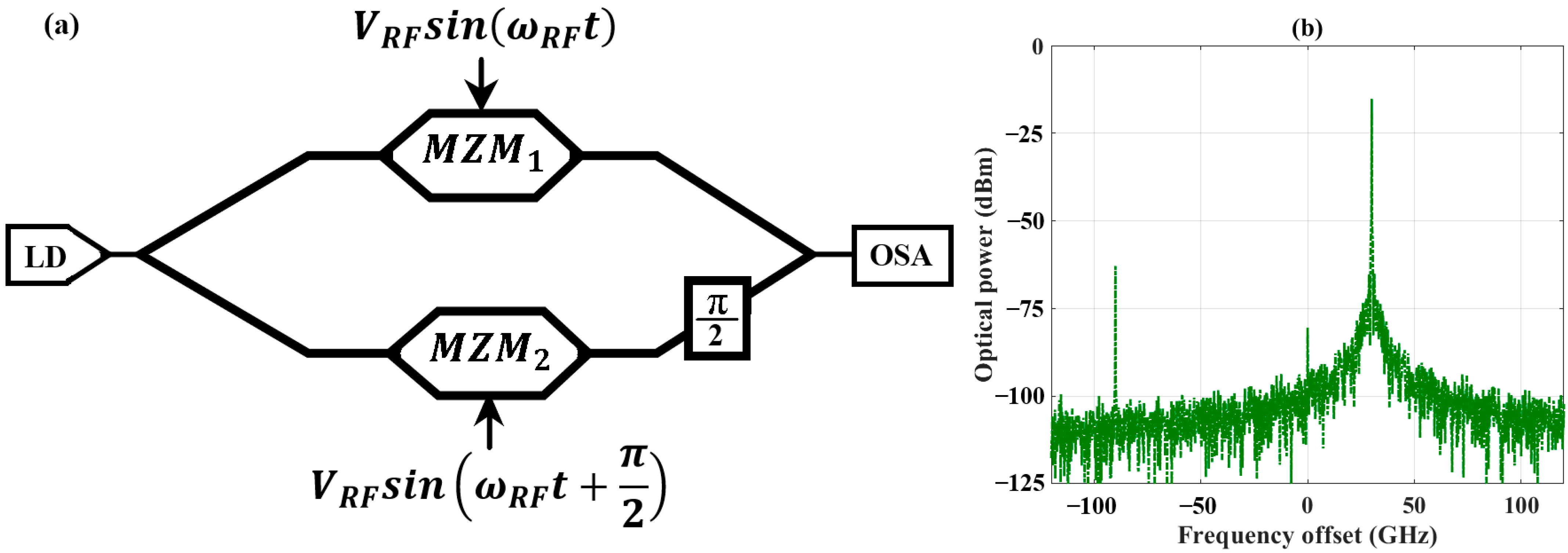
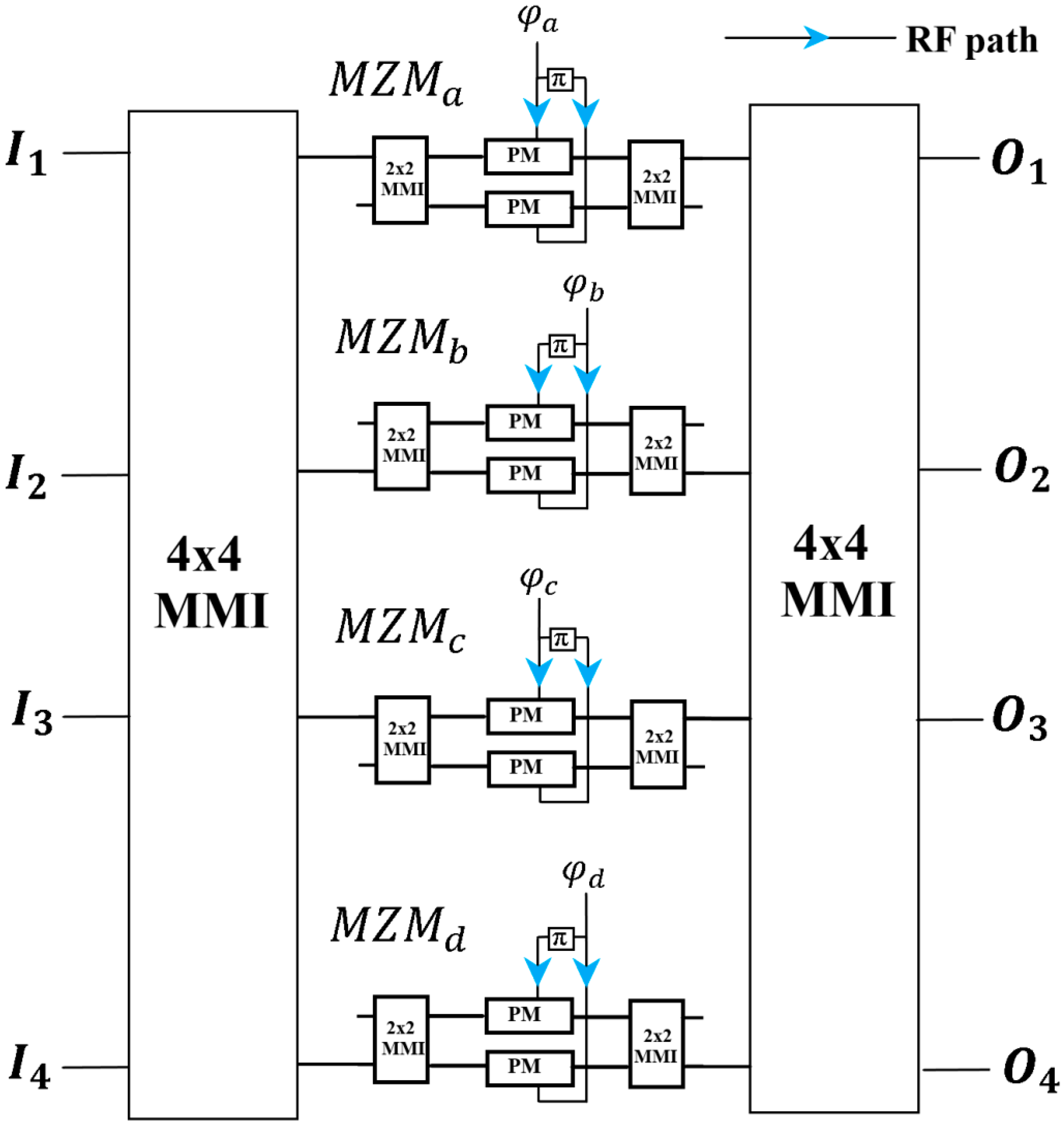
2. Theory
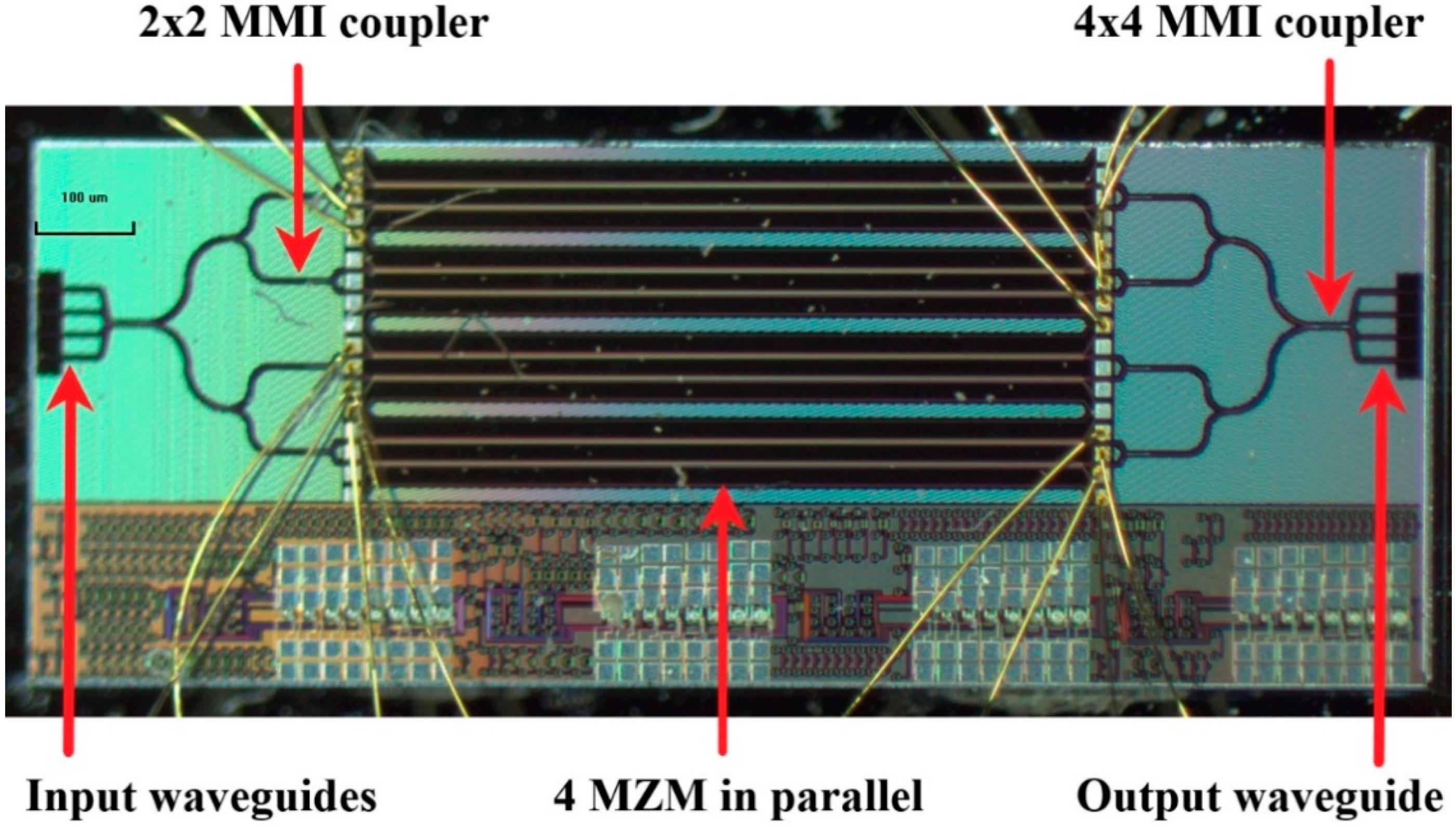
3. Device Fabrication
4. Experimental Result and Discussion
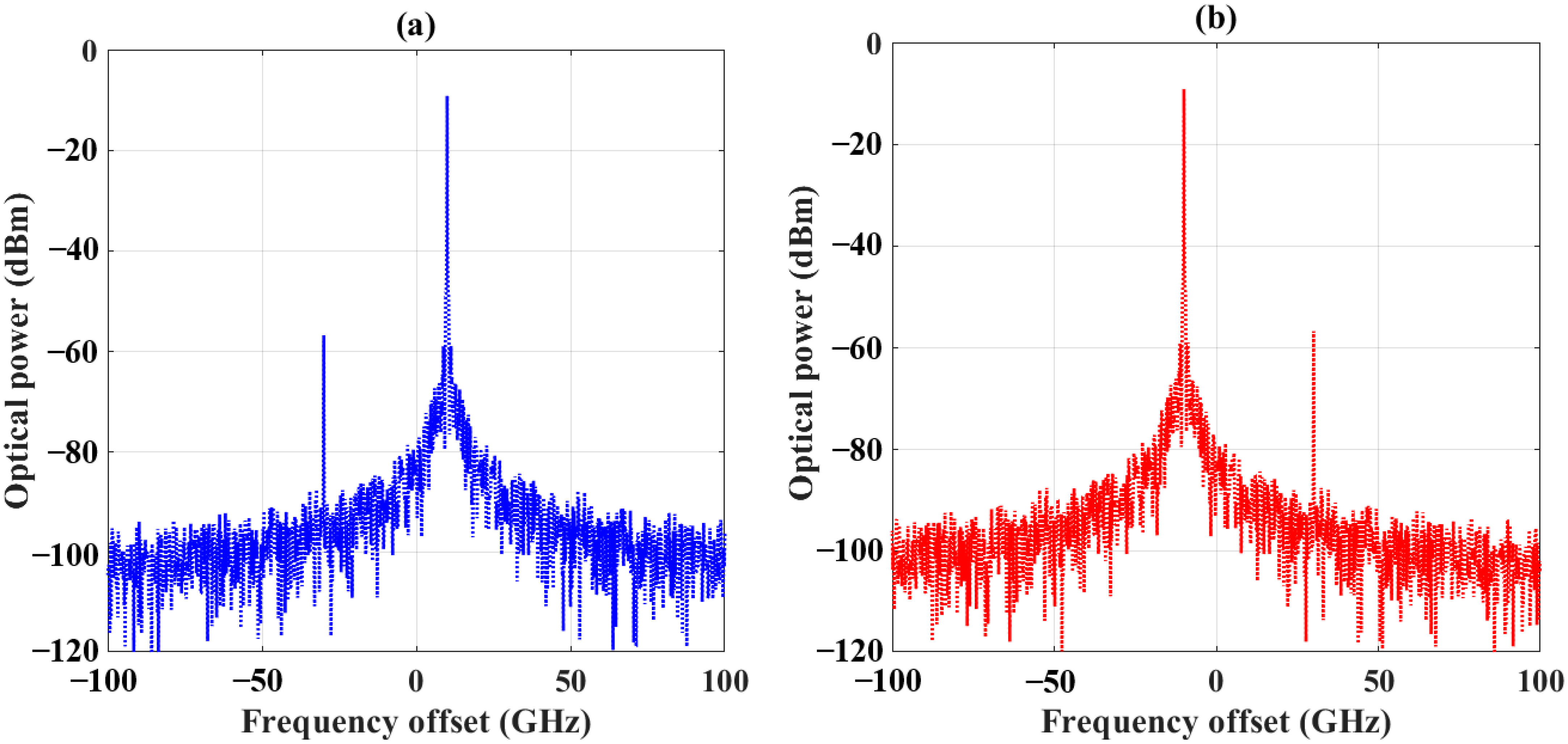
4.1. Static Assessment
4.2. Dynamic Assessment
5. Conclusions
Author Contributions
Funding
Institutional Review Board Statement
Informed Consent Statement
Data Availability Statement
Acknowledgments
Conflicts of Interest
References
- Hall, T.J.; Maldonado-Basilio, R.; Abdul-Majid, S.; Seregelyi, J.; Li, R.; Antolín-Pérez, I.; Nikkhah, H.; Lucarz, F.; Tocnaye, J.B.; Fracasso, B.; et al. Radio-over-Fibre access for sustainable Digital Cities. Ann. Telecommun. Ann. Télécommun. 2013, 68, 3–21. [Google Scholar] [CrossRef] [Green Version]
- Hirooka, T.; Yoshida, M.; Kasai, K.; Nakazawa, M. Optical and wireless-integrated next-generation access network based on coherent technologies. In Proceedings of the Broadband Access Communication Technologies X, San Francisco, CA, USA, 13–18 February 2016; Dingel, B.B., Tsukamoto, K., Eds.; SPIE OPTO: San Francisco, CA, USA, 2016; p. 977203. [Google Scholar]
- Kowalski, F.V.; Hale, P.D.; Shattil, S.J. Broadband continuous-wave laser. Opt. Lett. 1988, 13, 622–624. [Google Scholar] [CrossRef]
- Cygan, A.; Lisak, D.; Morzyński, P.; Bober, M.; Zawada, M.; Pazderski, E.; Ciuryło, R. Cavity mode-width spectroscopy with widely tunable ultra narrow laser. Opt. Express 2013, 21, 29744–29754. [Google Scholar] [CrossRef]
- Li, J.; Li, Z. Frequency-locked multicarrier generator based on a complementary frequency shifter with double recirculating frequency-shifting loops. Opt. Lett. 2013, 38, 359–361. [Google Scholar] [CrossRef]
- Li, J.; Zhang, X.; Li, Z.; Zhang, X.; Li, G.; Lu, C. Theoretical studies on the polarization-modulator-based single-side-band modulator used for generation of optical multicarrier. Opt. Express 2014, 22, 14087–14095. [Google Scholar] [CrossRef] [PubMed]
- Frankel, M.Y.; Esman, R.D.; Parent, M.G. Array transmitter/receiver controlled by a true time-delay fiber-optic beamformer. IEEE Photon. Technol. Lett. 1995, 7, 1216–1218. [Google Scholar] [CrossRef]
- Li, Y.; Meersman, S.; Baets, R. Optical frequency shifter on SOI using thermo-optic serrodyne modulation. In Proceedings of the 7th IEEE International Conference on Group IV Photonics, Beijing, China, 1–3 September 2010; IEEE: Piscataway, NJ, USA, 2010; pp. 75–77. [Google Scholar]
- Tanabe, T.; Notomi, M.; Kuramochi, E. Measurement of ultra-high-Q photonic crystal nanocavity using single-sideband frequency modulator. Electron. Lett. 2007, 43, 187–188. [Google Scholar] [CrossRef]
- Johnson, L.M.; Cox, C.H. Serrodyne optical frequency translation with high sideband suppression. J. Lightwave Technol. 1988, 6, 109–112. [Google Scholar] [CrossRef]
- Heismann, F.; Ulrich, R. Integrated-optical frequency translator with stripe waveguide. Appl. Phys. Lett. 1984, 45, 490–492. [Google Scholar] [CrossRef]
- Shen, Y.; Zhang, X.; Chen, K. Optical single sideband modulation of 11-GHz RoF system using stimulated Brillouin scattering. IEEE Photon. Technol. Lett. 2005, 17, 1277–1279. [Google Scholar] [CrossRef]
- Sharma, G.P.; Preußler, S.; Schneider, T. Precise optical frequency shifting using stimulated Brillouin scattering in optical Fibers. IEEE Photon. Technol. Lett. 2017, 29, 1467–1470. [Google Scholar] [CrossRef]
- Nosu, K.; Rashleigh, S.C.; Taylor, H.F.; Weller, J.F. Acousto-optic frequency shifter for single-mode fibres. Electron. Lett. 1983, 19, 816–818. [Google Scholar] [CrossRef]
- Cummins, H.Z.; Knable, N. Single sideband modulation of coherent light by Bragg reflection from acoustical waves. Proc. IEEE 1963, 51, 1246. [Google Scholar] [CrossRef]
- Hui, R.; Zhu, B.; Huang, R.; Allen, C.T.; Demarest, K.R.; Richards, D. Subcarrier multiplexing for high-speed optical transmission. J. Lightwave Technol. 2002, 20, 417. [Google Scholar]
- Frankel, M.Y.; Esman, R.D. Optical single-sideband suppressed-carrier modulator for wide-band signal processing. J. Lightwave Technol. 1998, 16, 859. [Google Scholar] [CrossRef]
- Xiao, S.; Weiner, A.M. Optical carrier-suppressed single sideband (O-CS-SSB) modulation using a hyperfine blocking filter based on a virtually imaged phased-array (VIPA). IEEE Photon. Technol. Lett. 2005, 17, 1522–1524. [Google Scholar] [CrossRef]
- Zibar, D.; Sambaraju, R.; Jambrina, A.C.; Alemany, R.; Herrera, J.; Monroy, I.T. 16 Gb/s QPSK Wireless-over-Fibre link in 75–110 GHz band employing optical heterodyne generation and coherent detection. In Proceedings of the 36th European Conference and Exhibition on Optical Communication, Turin, Italy, 19–23 September 2010; IEEE: Piscataway, NJ, USA, 2010; pp. 1–3. [Google Scholar]
- Izutsu, M.; Shikama, S.; Sueta, T. Integrated optical SSB modulator/frequency shifter. IEEE J. Quantum Electron. 1981, 17, 2225–2227. [Google Scholar] [CrossRef]
- Shimotsu, S.; Oikawa, S.; Saitou, T.; Mitsugi, N.; Kubodera, K.; Kawanishi, T.; Izutsu, M. Single side-band modulation performance of a LiNbO3 integrated modulator consisting of four-phase modulator waveguides. IEEE Photon. Technol. Lett. 2001, 13, 364–366. [Google Scholar] [CrossRef]
- Yamaguchi, Y.; Kanno, A.; Kawanishi, T.; Izutsu, M.; Nakajima, H. Pure single-sideband modulation using high extinction-ratio parallel Mach-Zehnder modulator with third-order harmonics superposition technique. In Proceedings of the Conference on Lasers and Electro-Optics (CLEO): Science and Innovations 2015, San Jose, CA, USA, 10–15 May 2015; Optical Society of America: Washington, DC, USA, 2015. [Google Scholar]
- Yamazaki, H.; Saida, T.; Goh, T.; Mori, A.; Mino, S. Dual-carrier IQ modulator with a complementary frequency shifter. Opt. Express 2011, 19, B69–B74. [Google Scholar] [CrossRef]
- Yamazaki, H.; Saida, T.; Goh, T.; Mino, S.; Nagatani, M.; Nosaka, H.; Murata, K. Dual-carrier dual-polarization IQ modulator using a complementary frequency shifter. IEEE J. Sel. Top. Quantum. Electron. 2013, 19, 175–182. [Google Scholar] [CrossRef]
- Chow, C.W.; Wang, C.H.; Yeh, C.H.; Chi, S. Analysis of the carrier-suppressed single-sideband modulators used to mitigate Rayleigh backscattering in carrier-distributed PON. Opt. Express 2011, 19, 10973–10978. [Google Scholar] [CrossRef]
- Lauermann, M.; Weimann, C.; Knopf, A.; Heni, W.; Palmer, R.; Koeber, S.; Elder, D.L.; Bogaerts, W.; Leuthold, J.; Dalton, L.R.; et al. Integrated optical frequency shifter in silicon-organic hybrid (SOH) technology. Opt. Express 2016, 24, 11694–11707. [Google Scholar] [CrossRef] [PubMed] [Green Version]
- Kodigala, A.; Gehl, M.; DeRose, C.T.; Hood, D.; Pomerene, A.T.; Dallo, C.; Trotter, D.; Moore, P.; Starbuck, A.L.; Lee, J.; et al. Silicon photonic single-sideband generation with dual-parallel mach-zehnder modulators. In Proceedings of the Conference on Lasers and Electro-Optics (CLEO): Science and Innovations 2019, San Jose, CA, USA, 5–10 May 2015; Optical Society of America: Washington, DC, USA, 2015. [Google Scholar]
- Hasan, M.; Hall, T.J. Photonic circuit for high order USB and LSB separation for remote heterodyning: Analysis and simulation. Opt. Express 2015, 23, 25259–25271. [Google Scholar] [CrossRef] [PubMed]
- Mao, M.Z.; Giddings, R.P.; Cao, B.Y.; Xu, Y.T.; Wang, M.; Tang, J.M. DSP-enabled reconfigurable and transparent spectral converters for converging optical and mobile fronthaul/backhaul networks. Opt. Express 2017, 25, 13836–13856. [Google Scholar] [CrossRef]
- Li, X.; Zhao, S.; Zhu, Z.; Qu, K.; Lin, T.; Pan, S. An optical frequency shifter based on high-order optical single-sideband modulation and polarization multiplexing. J. Lightwave Technol. 2016, 34, 5094–5100. [Google Scholar] [CrossRef]
- Xiao, X.; Li, S.; Xie, Z.; Peng, S.; Wu, D.; Xue, X.; Zheng, X.; Zhou, B. Photonic harmonic up-converter based on a self-oscillating optical frequency comb using a DP-DPMZM. Opt. Commun. 2018, 413, 48–53. [Google Scholar] [CrossRef]
- Ma, J.; Wen, A.; Tu, Z. Filter-free photonic microwave upconverter with frequency quadrupling. Appl. Opt. 2019, 58, 7915–7920. [Google Scholar] [CrossRef]
- Liow, T.Y.; Ang, K.W.; Fang, Q.; Song, J.F.; Xiong, Y.Z.; Yu, M.B.; Lo, G.Q.; Kwong, D.L. Silicon modulators and germanium photodetectors on SOI: Monolithic integration, compatibility, and performance optimization. IEEE J. Sel. Top. Quantum. Electron. 2009, 16, 307–315. [Google Scholar] [CrossRef]
- Miller, D.A. Perfect optics with imperfect components. Optica 2015, 2, 747–750. [Google Scholar] [CrossRef]
- Ortega-Moñux, A.; Alonso-Ramos, C.; Maese-Novo, A.; Halir, R.; Zavargo-Peche, L.; Pérez-Galacho, D.; Molina-Fernández, I.; Wangüemert-Pérez, J.G.; Cheben, P.; Schmid, J.H.; et al. An ultra-compact multimode interference coupler with a subwavelength grating slot. Laser Photonics Rev. 2013, 7, L12–L15. [Google Scholar] [CrossRef]
- Halir, R.; Bock, P.J.; Cheben, P.; Ortega-Moñux, A.; Alonso-Ramos, C.; Schmid, J.H.; Lapointe, J.; Xu, D.X.; Wangüemert-Pérez, J.G.; Molina-Fernández, Í.; et al. Waveguide sub-wavelength structures: A review of principles and applications. Laser Photonics Rev. 2015, 9, 25–49. [Google Scholar] [CrossRef]
- Cheben, P.; Schmid, J.H.; Wang, S.; Xu, D.X.; Vachon, M.; Janz, S.; Lapointe, J.; Painchaud, Y.; Picard, M.J. Broadband polarization independent nanophotonic coupler for silicon waveguides with ultra-high efficiency. Opt. Express 2015, 23, 22553–22563. [Google Scholar] [CrossRef] [PubMed]
- Picard, M.J.; Painchaud, Y.; Latrasse, C.; Larouche, C.; Pelletier, F.; Poulin, M. Novel spot-size converter for optical fiber to sub-μm silicon waveguide coupling with low loss, low wavelength dependence and high tolerance to alignment. In Proceedings of the 2015 European Conference on Optical Communication (ECOC), Valencia, Spain, 27 September–1 October 2015; IEEE: Piscataway, NJ, USA, 2015; pp. 1–3. [Google Scholar]


Publisher’s Note: MDPI stays neutral with regard to jurisdictional claims in published maps and institutional affiliations. |
© 2021 by the authors. Licensee MDPI, Basel, Switzerland. This article is an open access article distributed under the terms and conditions of the Creative Commons Attribution (CC BY) license (https://creativecommons.org/licenses/by/4.0/).
Share and Cite
Hasan, G.M.; Hasan, M.; Hall, T.J. Performance Analysis of a Multi-Function Mach-Zehnder Interferometer Based Photonic Architecture on SOI Acting as a Frequency Shifter. Photonics 2021, 8, 561. https://doi.org/10.3390/photonics8120561
Hasan GM, Hasan M, Hall TJ. Performance Analysis of a Multi-Function Mach-Zehnder Interferometer Based Photonic Architecture on SOI Acting as a Frequency Shifter. Photonics. 2021; 8(12):561. https://doi.org/10.3390/photonics8120561
Chicago/Turabian StyleHasan, Gazi Mahamud, Mehedi Hasan, and Trevor J. Hall. 2021. "Performance Analysis of a Multi-Function Mach-Zehnder Interferometer Based Photonic Architecture on SOI Acting as a Frequency Shifter" Photonics 8, no. 12: 561. https://doi.org/10.3390/photonics8120561