Photonic Crystal Enhanced by Metamaterial for Measuring Electric Permittivity in GHz Range

 ,
,
Abstract
:1. Introduction
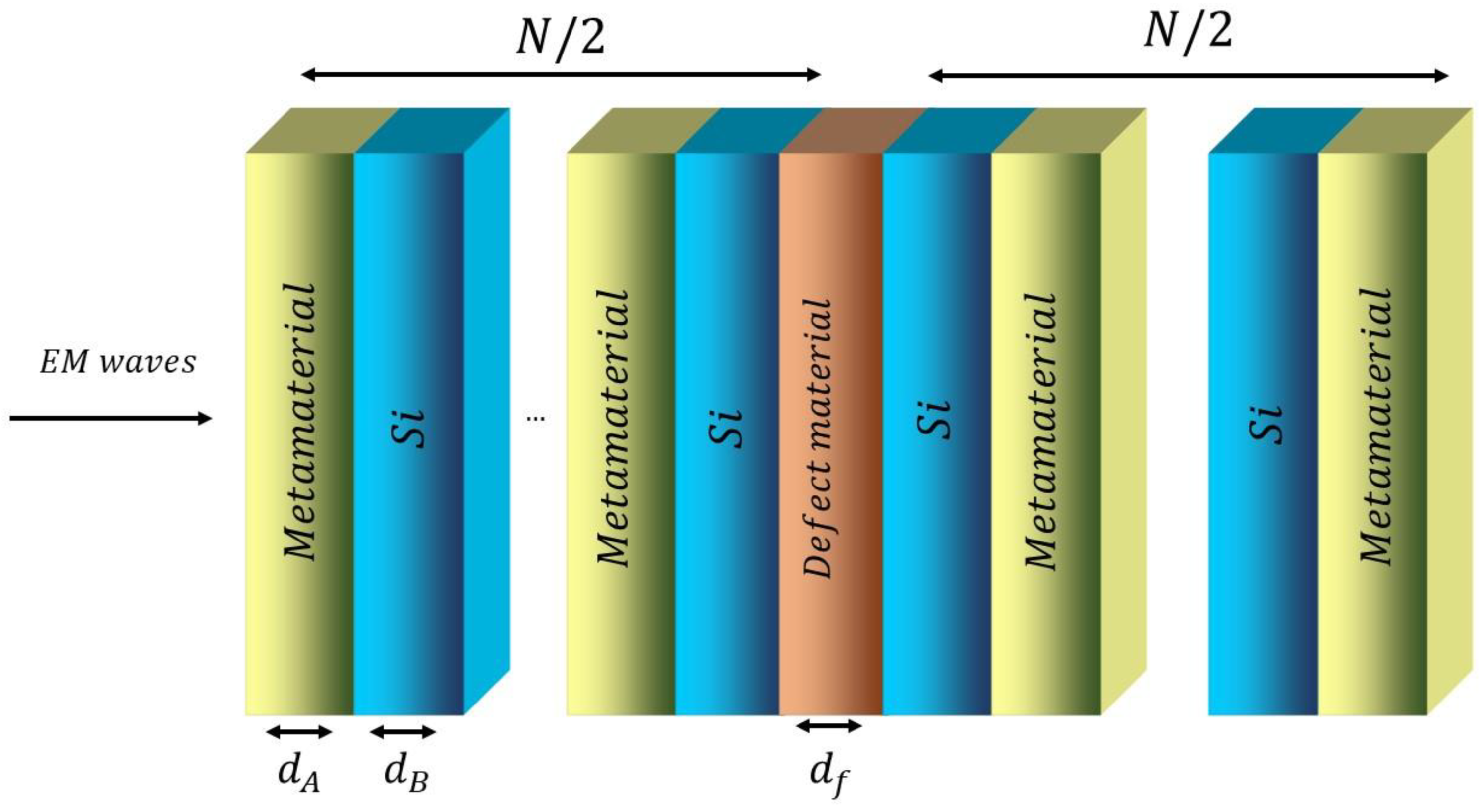
2. Theoretical Analysis
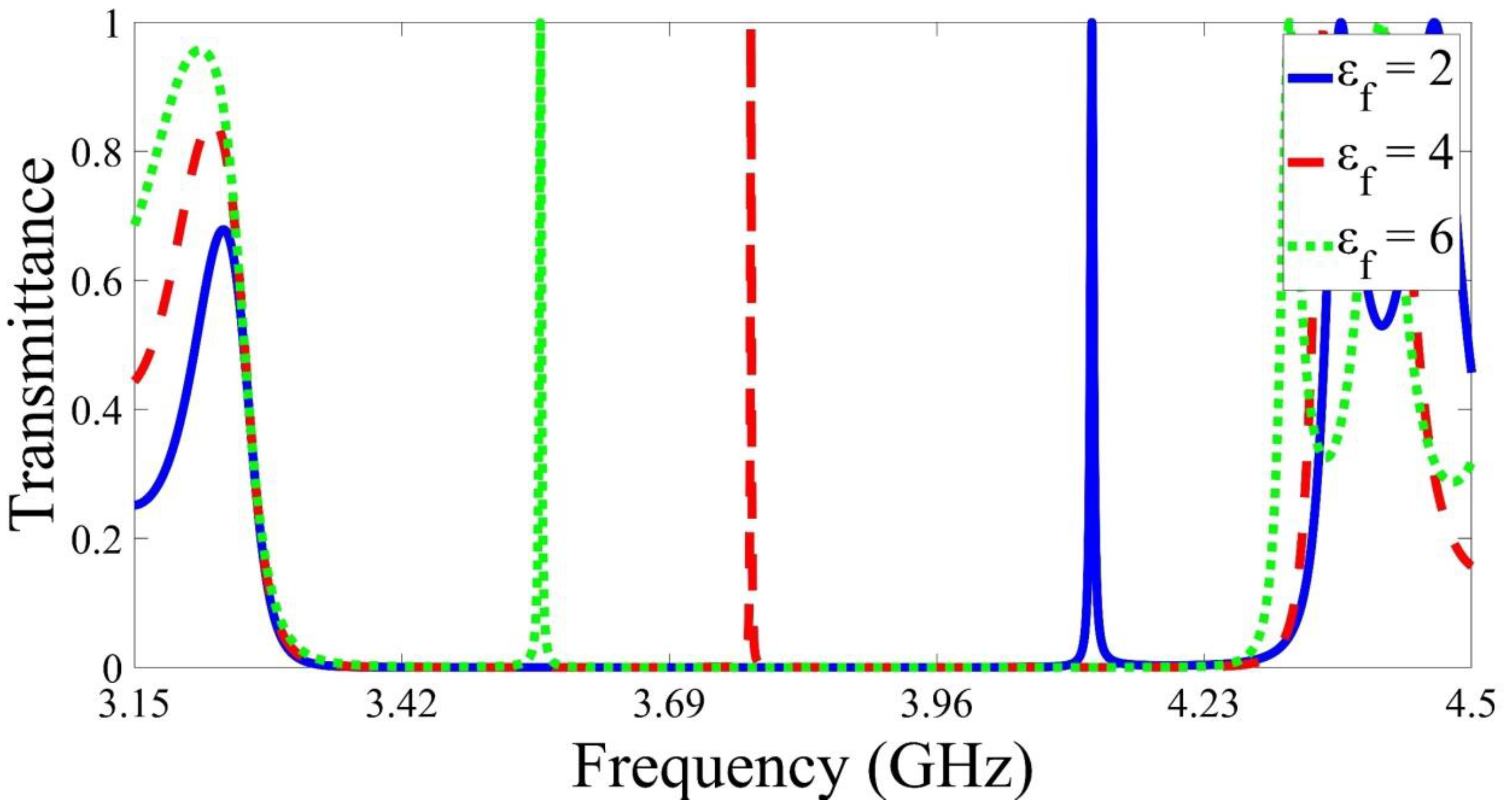
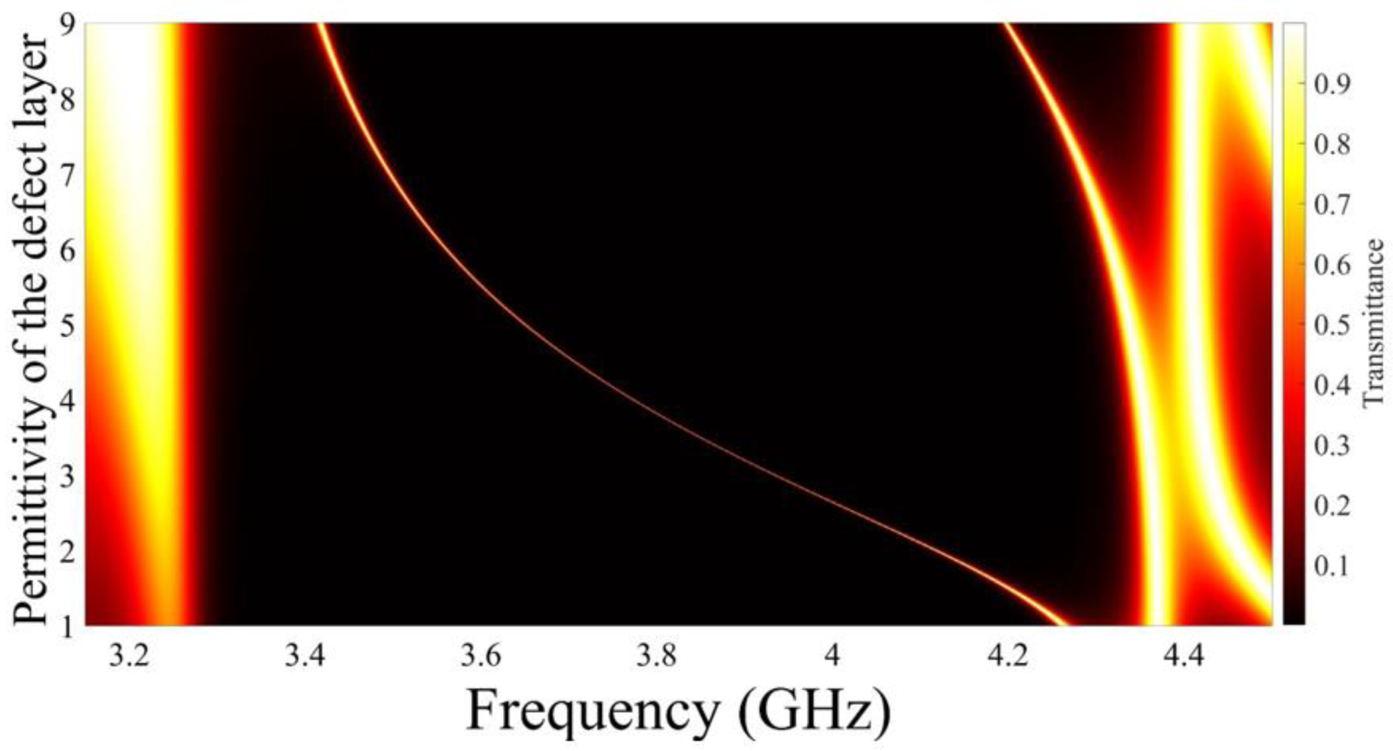
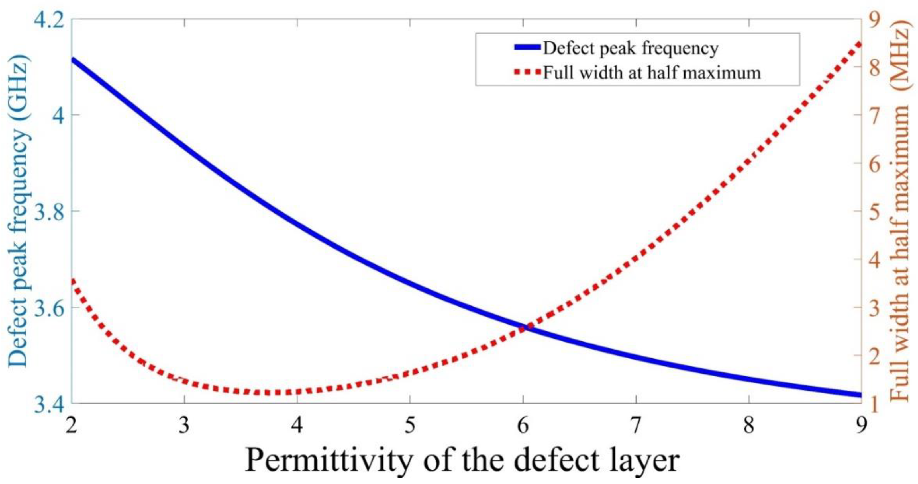
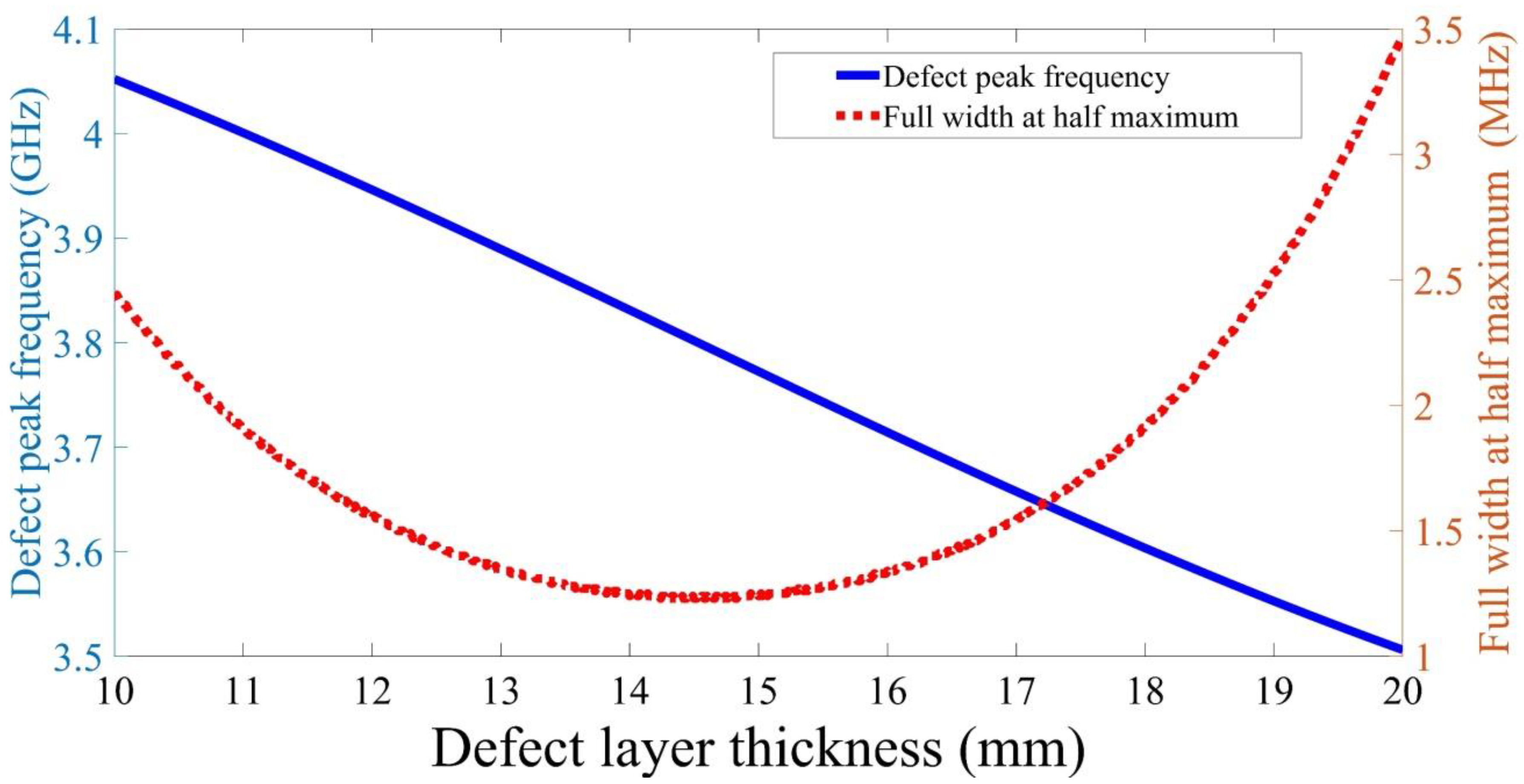
3. Results and Discussions
4. Conclusions
Author Contributions
Funding
Acknowledgments
Conflicts of Interest
References
- Noda, S.; Tomoda, K.; Yamamoto, N.; Chutinan, A. Full Three-Dimensional Photonic Bandgap Crystals at Near-Infrared Wavelengths. Science 2000, 289, 604–606. [Google Scholar] [CrossRef]
- Bayindir, M.; Temelkuran, B.; Ozbay, E. Propagation of photons by hopping: A waveguiding mechanism through localized coupled cavities in three-dimensional photonic crystals. Phys. Rev. B 2000, 61, R11855. [Google Scholar] [CrossRef] [Green Version]
- Bayindir, M.; Temelkuran, B.; Ozbay, E. Tight-Binding Description of the Coupled Defect Modes in Three-Dimensional Photonic Crystals. Phys. Rev. Lett. 2000, 84, 2140–2143. [Google Scholar] [CrossRef]
- Yablonovitch, E. Inhibited Spontaneous Emission in Solid-State Physics and Electronics. Phys. Rev. Lett. 1987, 58, 2059–2062. [Google Scholar] [CrossRef] [PubMed] [Green Version]
- John, S. Strong localization of photons in certain disordered dielectric superlattices. Phys. Rev. Lett. 1987, 58, 2486–2489. [Google Scholar] [CrossRef] [Green Version]
- Aly, A.H.; Ameen, A.A.; ElSayed, H.A.; Mohamed, S.H. Photonic crystal defective superconductor and black body radiations. Opt. Quantum Electron. 2018, 50, 361. [Google Scholar] [CrossRef]
- Manzanares-Martinez, J.; Archuleta-Garcia, R.; Castro-Garay, P.; Moctezuma-Enriquez, D.; Urrutia-Banuelos, E. One-Dimensional Photonic Heterostructure with Broadband Omnidirectional Reflection. Prog. Electromagn. Res. 2011, 111, 105–117. [Google Scholar] [CrossRef] [Green Version]
- Berman, O.L.; Lozovik, Y.E.; Eiderman, S.L.; Coalson, R.D. Superconducting photonic crystals: Numerical calculations of the band structure. Phys. Rev. B 2006, 74, 092505. [Google Scholar] [CrossRef]
- Moroz, A. Three-Dimensional Complete Photonic-Band-gap Structures in the Visible. Phys. Rev. Lett. 1999, 83, 5274–5277. [Google Scholar] [CrossRef]
- Kazmierczak, T.; Song, H.; Hiltner, A.; Baer, E. Polymeric One-Dimensional Photonic Crystals by Continuous Coextrusion. Macromol. Rapid Commun. 2007, 28, 2210–2216. [Google Scholar] [CrossRef]
- Aly, A.H.; Elsayed, H.A.; El-Naggar, S.A. Tuning the flow of light in two-dimensional metallic photonic crystals based on Faraday effect. J. Mod. Opt. 2017, 64, 74–80. [Google Scholar] [CrossRef]
- Akahane, Y.; Asano, T.; Song, B.-S.; Noda, S. High-Q photonic nanocavity in a two-dimensional photonic crystal. Nature 2003, 425, 944–947. [Google Scholar] [CrossRef]
- Chopra, H.; Kaler, R.S.; Painam, B. Photonic crystal waveguide-based biosensor for detection of diseases. J. Nanophotonics 2016, 10, 036011. [Google Scholar] [CrossRef]
- Poli, F.; Cucinotta, A.; Selleri, S. Photonic Crystal Fibers: Properties and Applications; Springer: Dordrecht, The Netherlands, 2007. [Google Scholar]
- Aly, A.H.; Elsayed, H.A.; Ameen, A.A.; Mohamed, S.H. Tunable properties of one-dimensional photonic crystals that incorporate a defect layer of a magnetized plasma. Int. J. Mod. Phys. B 2017, 31, 1750239. [Google Scholar] [CrossRef]
- del Villar, I.; Matias, I.; Arregui, F.; Claus, R. Analysis of one-dimensional photonic band gap structures with a liquid crystal defect towards development of fiber-optic tunable wavelength filters. Opt. Express 2003, 11, 430–436. [Google Scholar] [CrossRef]
- King, T.-C.; Yang, Y.-P.; Liou, Y.-S.; Wu, C.-J. Tunable defect mode in a semiconductor-dielectric photonic crystal containing extrinsic semiconductor defect. Solid State Commun. 2012, 152, 2189–2192. [Google Scholar] [CrossRef]
- Maurya, J.; François, A.; Prajapati, Y. Two-Dimensional Layered Nanomaterial-Based One-Dimensional Photonic Crystal Refractive Index Sensor. Sensors 2018, 18, 857. [Google Scholar] [CrossRef] [Green Version]
- Sreekanth, K.V.; Zeng, S.; Yong, K.-T.; Yu, T. Sensitivity enhanced biosensor using graphene-based one-dimensional photonic crystal. Sens. Actuators B Chem. 2013, 182, 424–428. [Google Scholar] [CrossRef]
- Villa-Arango, S.; Sánchez, D.B.; Torres, R.; Kyriacou, P.; Lucklum, R. Differential Phononic Crystal Sensor: Towards a Temperature Compensation Mechanism for Field Applications Development. Sensors 2017, 17, 1960. [Google Scholar] [CrossRef]
- Gharaati, A.; Zare, Z. Modeling of thermal tunable multichannel filter using defective metallic photonic crystals. Opt. Appl. 2017, 47, 611–619. [Google Scholar] [CrossRef]
- Aly, A.H.; Mohamed, D.; Matar, Z.S.; Trabelsi, Y.; Vigneswaran, D.; Tayeboun, F.; Mohaseb, M.A. Tunability and Fano Resonance Properties in Different Types of One-Dimensional Superconductor Photonic Crystals. Mater. Res. 2021, 24, e20200507. [Google Scholar] [CrossRef]
- Ameen, A.A.; ElSayed, H.; Aly, A.H. Towards a highly efficient air purifier using annular photonic crystals in UV regimes. RSC Adv. 2021, 11, 14915–14921. [Google Scholar] [CrossRef]
- Aly, A.H.; Elsayed, H.A. Defect mode properties in a one-dimensional photonic crystal. Phys. B Condens. Matter 2012, 407, 120–125. [Google Scholar] [CrossRef]
- Aly, A.H.; Ameen, A.A.; Vigneswaran, D. Superconductor Nanometallic Photonic Crystals as a Novel Smart Window for Low-Temperature Applications. J. Supercond. Nov. Magn. 2019, 32, 191–197. [Google Scholar] [CrossRef]
- Srivastava, S.K.; Aghajamali, A. Study of optical reflectance properties in 1D annular photonic crystal containing double negative (DNG) metamaterials. Phys. B Condens. Matter 2016, 489, 67–72. [Google Scholar] [CrossRef]
- Xu, W.; Xie, L.; Ying, Y. Mechanisms and applications of terahertz metamaterial sensing: A review. Nanoscale 2017, 9, 13864–13878. [Google Scholar] [CrossRef] [PubMed]
- Niu, X.; Hu, X.; Chu, S.; Gong, Q. Epsilon-Near-Zero Photonics: A New Platform for Integrated Devices. Adv. Opt. Mater. 2018, 6, 1701292. [Google Scholar] [CrossRef]
- Leonhardt, U.; Tyc, T. Broadband Invisibility by Non-Euclidean Cloaking. Science 2009, 323, 110–112. [Google Scholar] [CrossRef] [Green Version]
- Jacob, Z.; Alekseyev, L.V.; Narimanov, E. Optical Hyperlens: Far-field imaging beyond the diffraction limit. Opt. Express 2006, 14, 8247–8256. [Google Scholar] [CrossRef] [PubMed] [Green Version]
- Valentine, J.; Li, J.; Zentgraf, T.; Bartal, G.; Zhang, X. An optical cloak made of dielectrics. Nat. Mater. 2009, 8, 568–571. [Google Scholar] [CrossRef] [Green Version]
- Zhang, W.; Song, Q.; Zhu, W.; Shen, Z.; Chong, P.; Tsai, D.P.; Qiu, C.; Liu, A.Q. Metafluidic metamaterial: A review. Adv. Phys. X 2018, 3, 1417055. [Google Scholar] [CrossRef]
- Padilla, W.J.; Vier, D.C.; Nemat-Nasser, S.C.; Schultz, S.; Smith, D.R. Composite Medium with Simultaneously Negative Permeability and Permittivity. Phys. Rev. Lett. 2000, 84, 4184–4187. [Google Scholar] [CrossRef] [Green Version]
- Linden, S.; Enkrich, C.; Wegener, M.; Zhou, J.; Koschny, T.; Soukoulis, C.M. Magnetic Response of Metamaterials at 100 Terahertz. Science 2004, 306, 1351–1353. [Google Scholar] [CrossRef] [PubMed] [Green Version]
- Gundogdu, T.F.; Katsarakis, N.; Kafesaki, M.; Penciu, R.S.; Konstantinidis, G.; Kostopoulos, A.; Economou, E.N.; Soukoulis, C.M. Negative index short-slab pair and continuous wires metamaterials in the far infrared regime. Opt. Express 2008, 16, 9173–9180. [Google Scholar] [CrossRef] [PubMed]
- Valentine, J.; Zhang, S.; Zentgraf, T.; Ulin-Avila, E.; Genov, D.A.; Bartal, G.; Zhang, X. Three-dimensional optical metamaterial with a negative refractive index. Nature 2008, 455, 7211. [Google Scholar] [CrossRef]
- Li, J.; Zhou, L.; Chan, C.T.; Sheng, P. Photonic Band Gap from a Stack of Positive and Negative Index Materials. Phys. Rev. Lett. 2003, 90, 083901. [Google Scholar] [CrossRef] [PubMed]
- Aly, A.H.; Ameen, A.A.; Elsayed, H.A.; Mohamed, S.H.; Singh, M.R. One-Dimensional Metallo-Superconductor Photonic Crystals as a Smart Window. J. Supercond. Nov. Magn. 2019, 32, 2313–2318. [Google Scholar] [CrossRef]
- Yang, Y. Development of a Real-Time Ultra-Wideband See Through Wall Imaging Radar System. Doctoral Dissertations, The University of Tennessee, Knoxville, TN, USA, 2008. Available online: https://trace.tennessee.edu/utk_graddiss/432 (accessed on 31 December 2008).


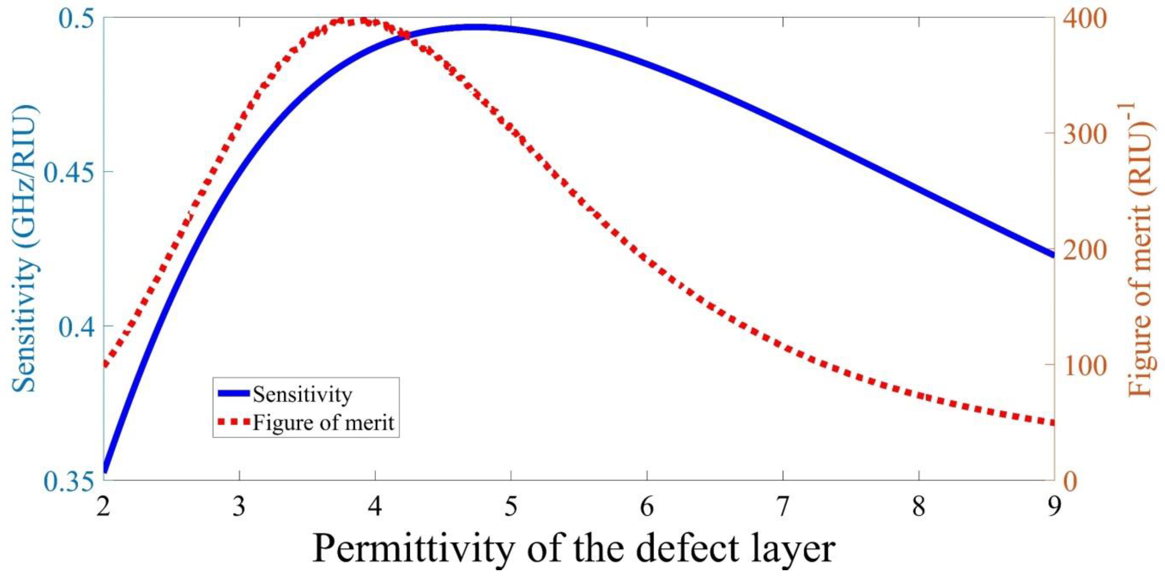
| 2 | 4.116 | 3.5 | 99.9% | 0.35 | 100.7 |
| 4 | 3.772 | 1.2 | 99.9% | 0.49 | 408.5 |
| 6 | 3.559 | 2.5 | 99.9% | 0.48 | 193.9 |
| Material | ||||||
|---|---|---|---|---|---|---|
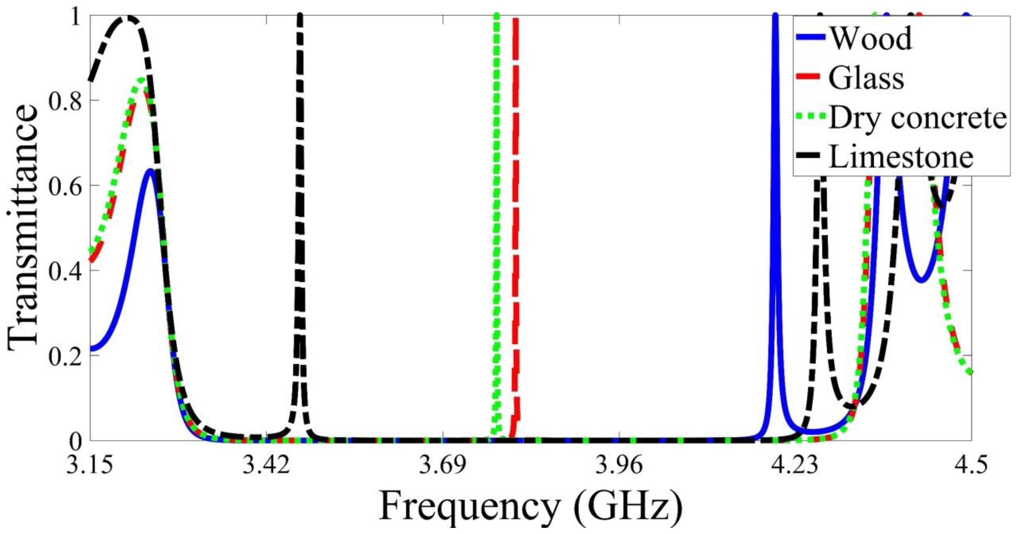
| Wood | 1.5 | 4.19 | 6.9 | 99.9% | 0.282 | 40.9 |
| Glass | 3.8 | 3.80 | 1.2 | 99.9% | 0.485 | 404.6 |
| Dry concrete | 4 | 3.77 | 1.2 | 99.9% | 0.490 | 408.5 |
| Limestone | 7.5 | 3.47 | 4.9 | 99.9% | 0.455 | 92.8 |
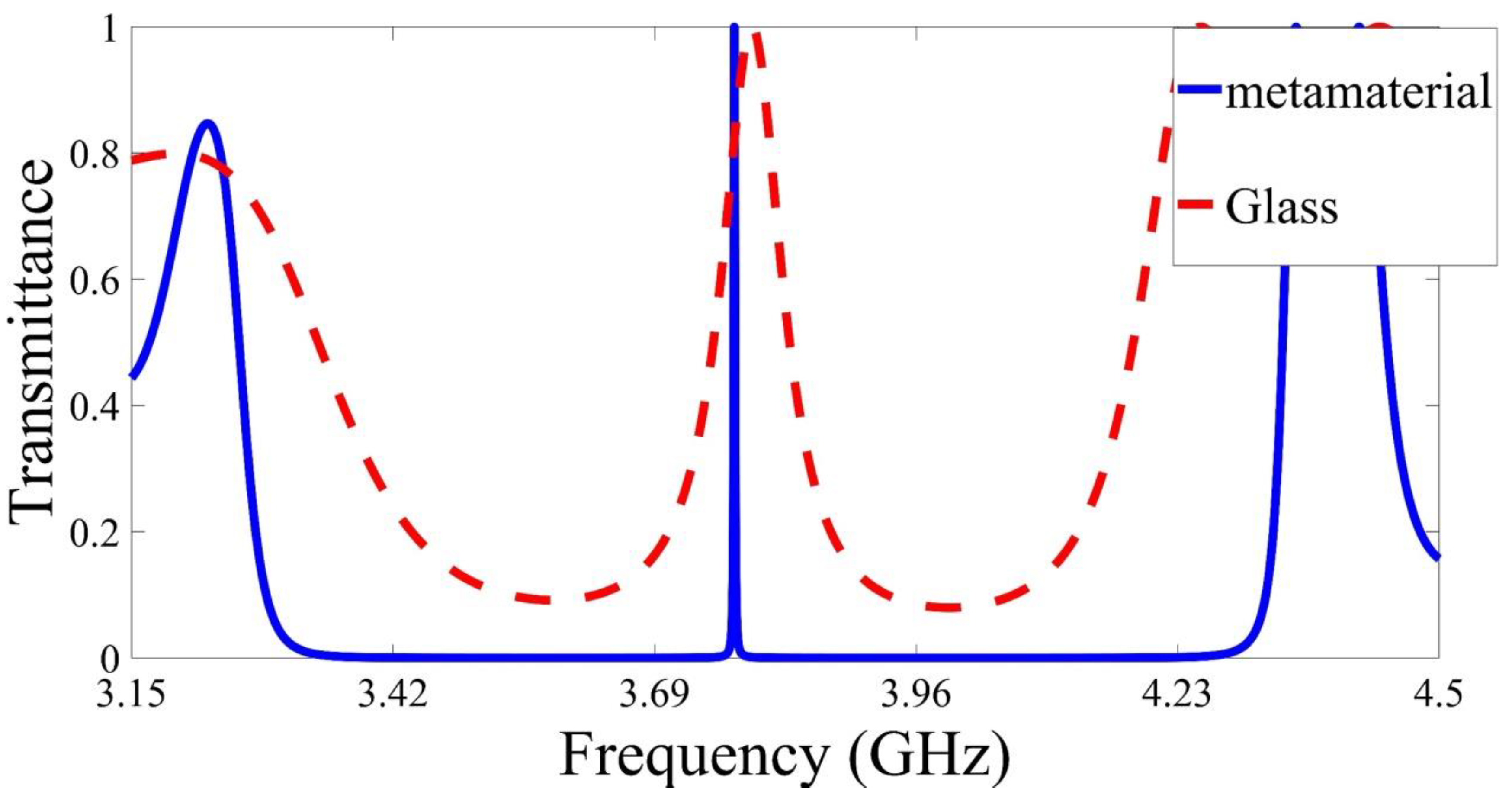
| Material | N | Q | |||
|---|---|---|---|---|---|
| Metamaterial | 6 | 3.77 | 1.2 | 99.9% | 3143.6 |
| Glass | 6 | 3.79 | 86 | 99.9% | 44.06 |
| Glass | 16 | 3.77 | 1.6 | 99.9% | 2356.2 |
Publisher’s Note: MDPI stays neutral with regard to jurisdictional claims in published maps and institutional affiliations. |
© 2021 by the authors. Licensee MDPI, Basel, Switzerland. This article is an open access article distributed under the terms and conditions of the Creative Commons Attribution (CC BY) license (https://creativecommons.org/licenses/by/4.0/).
Share and Cite
Aly, A.H.; Ameen, A.A.; Mahmoud, M.A.; Matar, Z.S.; Al-Dossari, M.; Elsayed, H.A. Photonic Crystal Enhanced by Metamaterial for Measuring Electric Permittivity in GHz Range. Photonics 2021, 8, 416. https://doi.org/10.3390/photonics8100416
Aly AH, Ameen AA, Mahmoud MA, Matar ZS, Al-Dossari M, Elsayed HA. Photonic Crystal Enhanced by Metamaterial for Measuring Electric Permittivity in GHz Range. Photonics. 2021; 8(10):416. https://doi.org/10.3390/photonics8100416
Chicago/Turabian StyleAly, Arafa H., Ayman A. Ameen, M. A. Mahmoud, Z. S. Matar, M. Al-Dossari, and Hussein A. Elsayed. 2021. "Photonic Crystal Enhanced by Metamaterial for Measuring Electric Permittivity in GHz Range" Photonics 8, no. 10: 416. https://doi.org/10.3390/photonics8100416