Photonic Band Gaps and Resonance Modes in 2D Twisted Moiré Photonic Crystal


1
Department of Physics, University of North Texas, Denton, TX 76203, USA
2
Department of Electrical Engineering, University of North Texas, Denton, TX 76203, USA
*
Author to whom correspondence should be addressed.
Photonics 2021, 8(10), 408; https://doi.org/10.3390/photonics8100408
Submission received: 9 September 2021
/
Revised: 19 September 2021
/
Accepted: 20 September 2021
/
Published: 23 September 2021
(This article belongs to the Special Issue Design and Application of Modern Evanescent Wave Photonic Sensors)
Abstract
:The study of twisted bilayer 2D materials has revealed many interesting physics properties. A twisted moiré photonic crystal is an optical analog of twisted bilayer 2D materials. The optical properties in twisted photonic crystals have not yet been fully elucidated. In this paper, we generate 2D twisted moiré photonic crystals without physical rotation and simulate their photonic band gaps in photonic crystals formed at different twisted angles, different gradient levels, and different dielectric filling factors. At certain gradient levels, interface modes appear within the photonic band gap. The simulation reveals “tic tac toe”-like and “traffic circle”-like modes as well as ring resonance modes. These interesting discoveries in 2D twisted moiré photonic crystal may lead toward its application in integrated photonics.
1. Introduction
Reducing the dimensionality of a material system very often leads to exceptional electronic, optical, and magnetic properties because of enhanced quantum effects in reduced phase space [1]. Recently, atomically thin two-dimensional (2D) materials have been stacked layer-by-layer to create synthetic materials with entirely new properties [2]. Intensive research has been focused on moiré materials where 2D layered materials are superposed against each other with a relative twist angle [3,4,5,6,7,8,9,10,11,12,13,14,15,16,17,18]. The formed moiré pattern at different twist angles results in a topological edge state, the formation of moiré excitons, interlayer magnetism, and fine control of the electron band structure [3,4,5,6,7,8,9,10,11,12,13,14,15,16,17,18]. In particular, the recent discovery of superconductivity in magic-angle twisted bilayer graphene [4] has triggered another wave of research in moiré 2D materials [5,6,7,8,9,10,11,12,13,14,15,16,17,18].
Twisted moiré photonic crystal is an optical analog of twisted 2D materials while photonic crystal is a periodic dielectric structure with a modulation of the refractive index close to the operation wavelength of light [19,20,21]. The twisted bilayer photonic crystal consists of two layers of identical photonic crystal stacked into moiré patterns [19,22,23,24] that also revealed magic-angle photonic flat bands with a non-Anderson-type localization [23]. Several research groups have generated twisted photonic crystals in photorefractive crystals with a shallow refractive index modulation and have observed the localization and delocalization of light waves [25,26,27,28,29,30,31].
Moiré photonic crystals have also been fabricated by holographic fabrication through laser interference of two sets of laser beams arranged in two-cone geometry with different cone angles [31,32,33,34,35,36,37,38]. Due to the gradient pattern and super-cell in the photonic crystal, this has also been named graded photonic super-crystal [37,38,39] or graded photonic super-quasi-crystal [35]. In contrast to twisted bilayer 2D materials and twisted bilayer photonic crystal, two mutually twisted optical lattices generated by laser interference will interfere further and form a single layer twisted photonic crystal if we consider the 2D case [36].
In this paper, we show the relationship between moiré pattern and twisted holographic pattern. Due to three-dimensional (3D) feature in the formed holographic pattern, there are different modulation levels at different z-locations and, thus, different gradients in the x–y plane. We simulate the photonic band structure and resonance modes for 2D twisted photonic crystal formed at different z-locations. There are interface modes within the photonic band gap at certain z-locations. Interestingly, crossing the waveguide along the interface, ring resonator, and their combination appears at different frequencies in the simulation of electric-field intensity for resonance modes in the 2D twisted moiré photonic crystal.
2. Design Principle from a Moiré Pattern with a Physical Rotation to a Twisted Holographic Photonic Crystal without Physical Rotations
The design principle of twisted photonic crystals comes from the analysis of reciprocal spatial and frequency (spectral) domains of the moiré pattern and the application of such an analysis to the real and reciprocal k-space in the optical lattice.
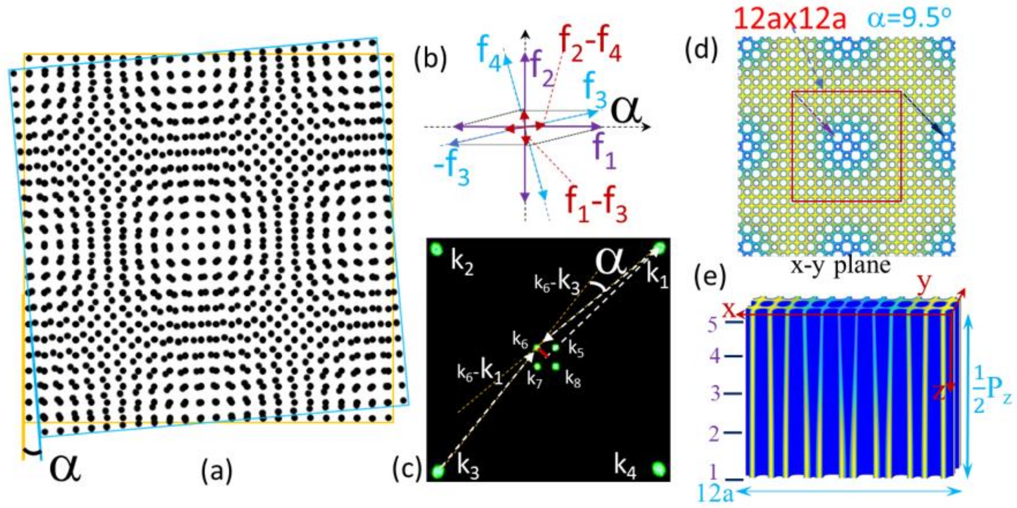
Figure 1a shows the superposition of 2D square dot patterns in the spatial domain, as an example, with a twist angle of α. The square dot pattern edged by a yellow square in Figure 1a has two fundamental frequency vectors f1 and f2 in the spectral domain in the Fourier transform. These two frequency vectors are perpendicular and have the same magnitude as shown in Figure 1b. The spectra of Fourier transform have …, −3f1, −2f1, −f1, 0, f1, 2f1, 3f1, … and −3f2, −2f2, −f2, 0, f2, 2f2, 3f2, …, etc. [40]. Only frequency vectors of −f1, f1 and −f2, f2 are drawn in purple arrows in Figure 1b. For the square dot pattern edged by a blue square, only frequency vectors of −f3, f3 and −f4, f4 are drawn in blue arrows in Figure 1b. The f3 and f4 vectors are perpendicular and have the same magnitude. The frequencies of f1–f3 and f2–f4 in Figure 1b are within the visible circle [40].
The spectra with frequencies of f1–f3 and f2–f4 represent the visible periodic component in the spatial domain in Figure 1a. The index for a moiré pattern is defined by, for example, f1−f3 = (1f1 + 0f2 − f3 + 0f4) => (1, 0, −1, 0) [40]. Thus, Figure 1a shows a moiré pattern with an index of (1, 0, −1, 0) and (0, 1, 0, −1) in the superposition of two square dot patterns with a twist angle of α. The moiré frequency (f1–f3) can be calculated by Equation (1)
A similar analysis is applied to the holographic pattern below. When eight beams (eight 532 nm green spots in Figure 1c) are overlapped through a 4f imaging system [34], these four inner beams together with four outer beams have holographic interference with an intensity I(r) calculated by Equation (2):
where e is the electric field polarization, E is the electric field, k is the wave vector, and δ is the initial phase. The orientation of the optical lattice in real space is determined by the vector difference of (ki–kk) in reciprocal space. (k1,k2,k3,k4) in Figure 1c are the k-vector components in the x–y plane for outer beams and have the same magnitude while (k5,k6,k7,k8) are the k-vector components in the x–y plane for inner beams and have also the same magnitude. From Figure 1c, we can see that the k-vector difference (k1–k6) is twisted by a rotation angle α from (k3–k6).
There is the same twist angle between (k2–k7) and (k4–k7), between (k3–k8) and (k1–k8), and between (k4–k5) and (k2–k5). By analyzing the cross-section in the x–y plane of the formed 3D holographic pattern, a square optical lattice in real space due to reciprocal k-vectors of (k1–k6), (k2–k7), (k3–k8), and (k4–k5) is twisted by a rotation angle α from those by (k3–k6), (k4–k7), (k1–k8), and (k2–k5). The twist angle α is determined by the ratio of the k-vector component in th4 x–y plane of the inner beam over the outer beam in Equation (3):
Figure 1d shows a simulated twisted 2D holographic photonic crystal in the x–y plane. A super-cell appears in the figure as indicated by red solid square. The size(s) of the super-cell is approximately determined by Equation (4):
and lattice period a is approximately calculated by Equation (5):
Thus, the size of super-cell is related to lattice period a and twist angle α by Equation (6):
The period in the z-direction (Pz) of the 3D holographic pattern is determined by the z-components of inner and outer beams, ki,z and ko,z, respectively, in Equation (7):
Figure 1d shows simulated 2D moiré photonic crystal in the x–y plane with a twist angle of 9.5 degrees and super-cell size of 12a × 12a as indicated by the solid red square. The central area of the red square in Figure 1d is a bright region, and the others are dark regions. Figure 1e shows a 3D interference pattern with dimensions of 12a × 2a × 0.5 Pz. These two figures are inverted structures from the interference assuming a positive photoresistor is used. Figure 1d is a cross section at z = 0.17 Pz from the bottom of Figure 1e.
Thus, by arranging the two sets of interfering beams in two-cone geometry and controlling the cone angle, we are able to relate the moiré pattern to the twist photonic crystal. Those graded photonic super-crystals [31,33,34,37] generated by two-cone arrangement of the laser beam are actually 2D twisted photonic crystals.
3. Simulation Methods
We simulate photonic band gap and resonance modes for 2D twist moiré photonic crystal obtained at different z-locations of 1, 2, 3, 4, and 5 in Figure 1e and also at different iso-intensity surface by setting up the intensity threshold. In the simulation, the interference intensity function, I(r), in Equation (2) at certain z-location, is replaced by a binary Si/air structures by comparing I(r) with a threshold intensity Ith. A step function is used: ε(r) = 1 (for air) when I > Ith, and ε(r) = 12 (for Si) when I < Ith. Photonic band structures in 2D twisted moiré photonic crystal with air holes in Si were computed using the MIT Photonic Bands (MPB) software package, a fully-vectorial eigenmode solver for Maxwell’s equations [41], via the Simpetus Electromagnetic Simulation Platform from Amazon Web Services.
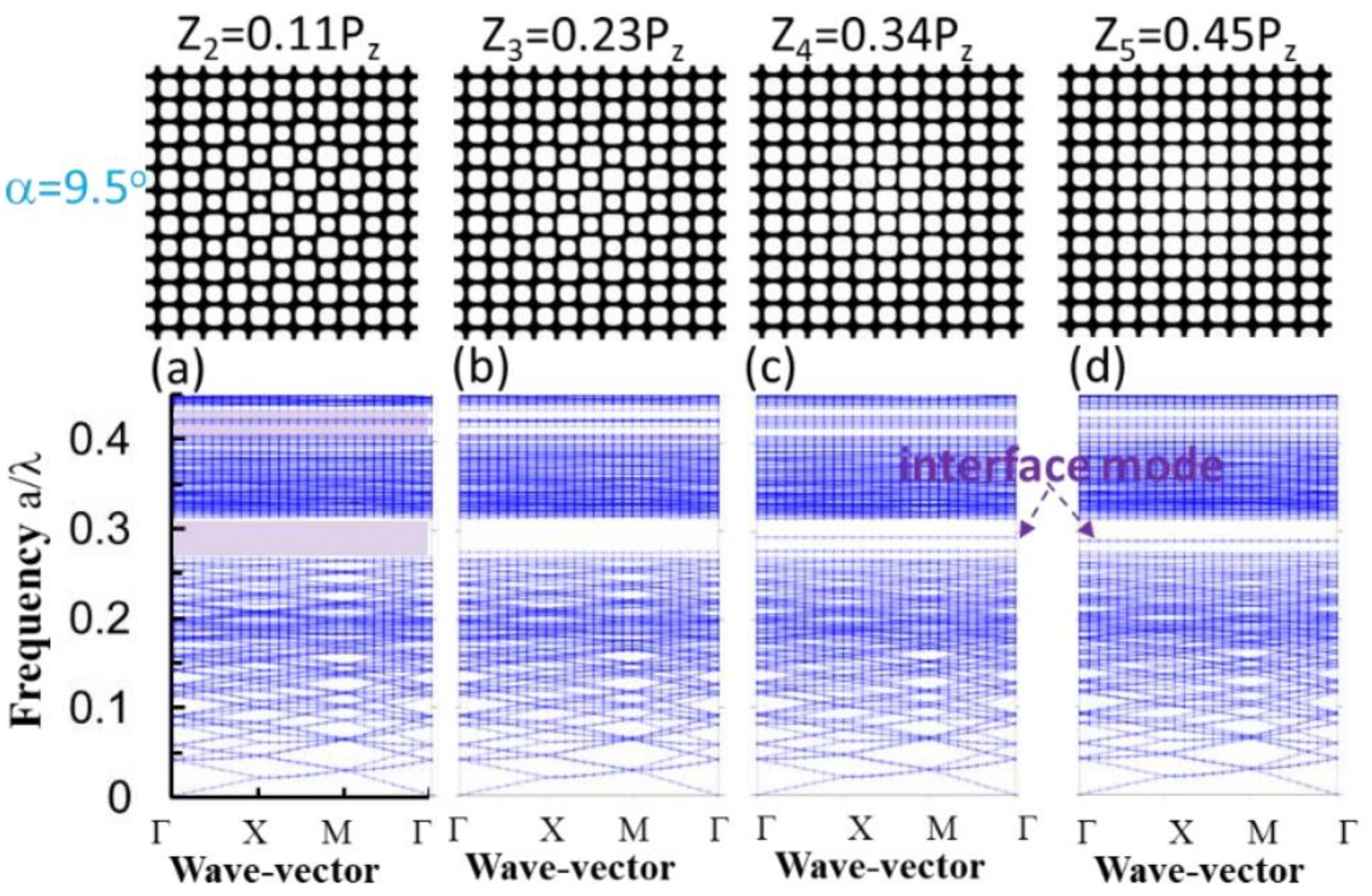
The spatial distribution of dielectric constants was output from MPB and is shown in top row in Figure 2 at different z-locations of 0.11, 0.23, 0.34, and 0.45 Pz in location 2, 3, 4, and 5 in Figure 1e, respectively. We also simulate cavity quality factors and electric field (E-field) intensity distributions for resonance modes in twisted photonic crystal with a thickness of 2a using the harmonic inversion function included in the MIT MEEP software [42,43] via Amazon Web Services.
4. Results
4.1. Photonic Band Structures in Twisted Photonic Crystals with Different z-Locations, Twist Angle and Threshold Intensity in the Step Function
We simulated photonic band structures in moiré photonic crystals with a twist angle of 9.5 degrees obtained at various z-locations. Figure 2a–d shows the results for TE modes in the twisted moiré photonic crystals at z = 0.11, 0.23, 0.34, and 0.45 Pz, respectively. The smaller the z-location in Figure 2, the higher the gradient level is. The shadowed areas in Figure 2a indicate the photonic crystal gaps. Figure 2a shows three photonic band gaps around frequency a/λ of 0.26–0.31, 0.4–0.42, and 0.43–0.44. With increasing z-location, the size of all three band gaps decreases and the frequency ranges of the photonic band gaps are almost same. However, interface modes (or waveguide mode for wave propagation) appear within the lowest photonic band gap in Figure 2c,d. The photonic band gap around 0.4–0.41 disappears at z-location = 0.45 Pz in Figure 2d.
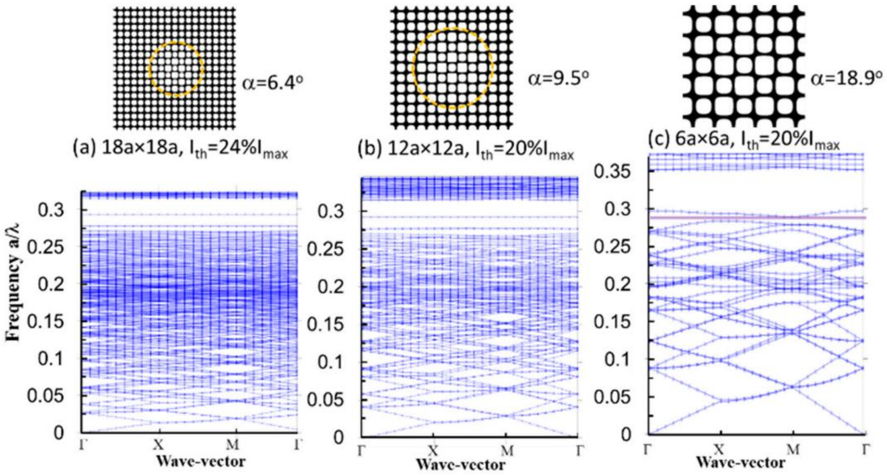
Figure 3 shows the photonic band structure for TE modes in moiré photonic crystals with twist angles of 6.4, 9.5, and 18.9 degrees at a z-location around 0.4 Pz. In Figure 3a,b, the photonic band gap appears at almost the same frequency range and almost the same gap size. Interface modes appear in both Figure 3a,b. In the unit super-cell of 12a × 12a in Figure 3b, half of the lattices are inside the yellow circle (bright region). Both dark and bright regions have contribution to the formation of the photonic band gap and interface mode. An increase of the unit super-cell to 18a × 18a in Figure 3a only increases the dark region outside the yellow circle. However, almost all regions are considered as bright regions in the unit super-cell of 6a × 6a in Figure 3c.
The photonic band gap increases and the interface mode is not flat and close to the band-edge above the shadowed area in Figure 3c. Other optical properties, such as the extraction efficiency of organic light emitting diode patterned in moiré photonic crystal, reaches high performance in moiré photonic crystal with unit super-cell sizes between 9a × 9a and 14a × 14a [44]. It is not necessary to have a twisted photonic crystal with a very large unit super-cell in order to gain different properties from traditional photonic crystals. Below, we focus our research on the moiré photonic crystal with a twist angle of 9.5 degrees (super-cell of 12a × 12a).
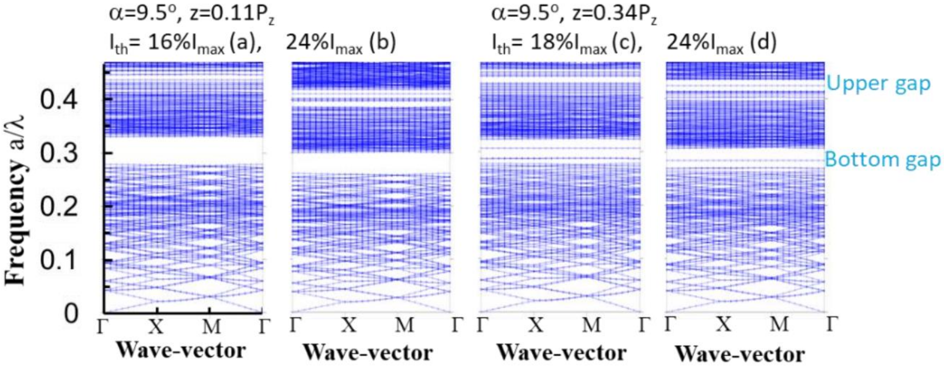
We simulated photonic band structures for moiré photonic crystals with a twist angle of 9.5 degrees, obtained by setting the threshold Ith in the range of 16% Imax and 26% Imax in the step function and at z-locations of 0.11, 0.23, 0.34, and 0.45 Pz. Representative results for twisted photonic crystals with z = 0.11 Pz, Ith = 16% Imax, and 24% Imax are shown in Figure 4a,b, and with z = 0.34 Pz, Ith = 18% Imax, and 24% Imax in Figure 4c,d, respectively. With increasing threshold intensity, both filling fraction of dielectric materials and effective refractive index of the twisted photonic crystal will increase.
The central wavelength for the Bragg diffraction from the twisted photonic crystal will also increases. Thus, the central frequency of the photonic band gap decreases as shown in Figure 4. The band gap width also decreases with increasing the threshold intensity. By varying Ith, the bottom photonic band gap does not have an interface mode for twisted photonic crystals obtained at z = 0.11 and 0.23 Pz, and there is always an interface mode in the bottom band gap for those obtained at z = 0.34 and 0.45 Pz. However, the band gap splits and interface modes appear in the upper band gap with increasing Ith for all z locations.
4.2. Resonance Modes in Twisted Photonic Crystals at Different z-Locations
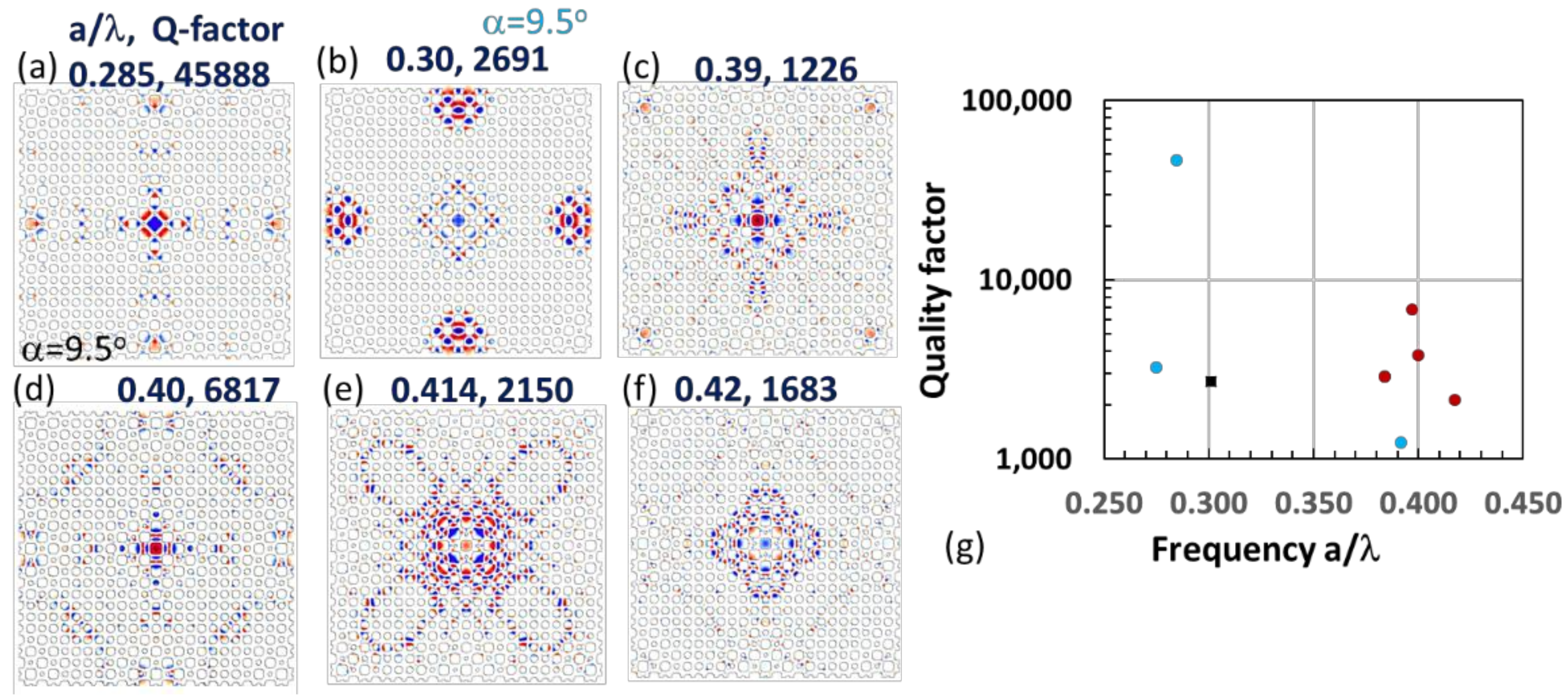
We simulate quality-factors (Q-factors) and electric-field intensity distribution for resonance modes in two moiré photonic crystals where one has no interface mode and the other has an interface mode in the bottom band gap. Figure 5a–f shows the electric-field intensity for resonance and interface modes at frequency a/λ of 0.285, 0.30, 0.39, 0.40, 0.414, and 0.42 with a Q-factor of 45,888, 2691, 1226, 6817, 2150, and 1683, respectively, for moiré photonic crystal with a twist angle of 9.5 degrees at z = 0.11 Pz.
Due to the dislocation in the bottom band gap [38] between the bright and dark regions in the moiré photonic crystal, some resonance modes appear in the bright region with a high Q-factor as shown in Figure 5a. The resonance or waveguide modes in Figure 5c–f are related to the interface modes in the upper band gap. They have a square symmetry with oscillations in the x and y directions in Figure 5c, in the diagonal direction in 5f and in both x (or y) and diagonal directions in Figure 5d,e. Figure 5g shows the Q-factors for resonance and interface modes at certain frequency locations. The purple square and red circles in the figure indicate these modes near the band gap edges or within the interface state.
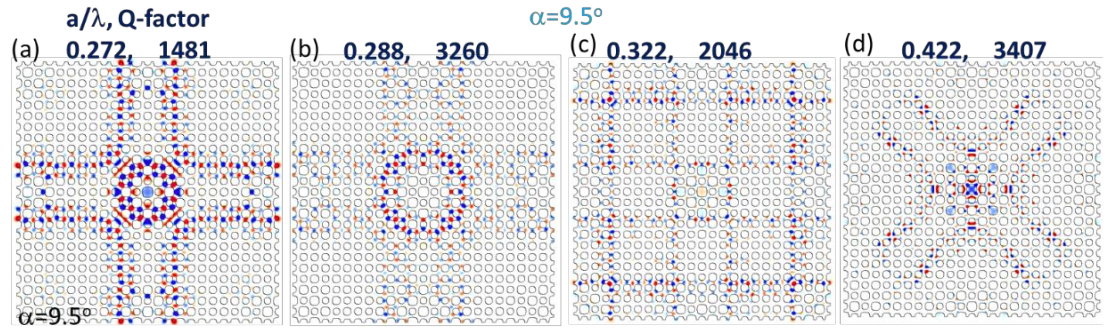
Figure 6 shows the electric-field intensity distribution for interface (or waveguide) modes at frequencies a/λ of 0.272, 0.288, 0.322, and 0.422 with a Q-factor of 1481, 3260, 2046, and 3407, respectively, for moiré photonic crystal with a twist angle of 9.5 degrees at z = 0.34 Pz. Due to the small gradient in the moiré pattern at z = 0.34 Pz and interface modes within both bottom and upper band gaps, wave propagation into the moiré photonic crystal is expected. High symmetry “traffic circle”-like waveguides and ring resonators are observed in Figure 6a at a frequency a/λ of 0.272, close to the frequency for the interface mode within the bottom band gap. Figure 6b shows a ring resonator around the edge of the bright region in the moiré photonic crystal at a frequency a/λ of 0.288. Square symmetry “tic tac toe”-like wave propagation is shown in Figure 6c at a frequency a/λ of 0.322, near the gap edge of bottom band gap. The “x” shape resonance mode in Figure 6d corresponds to the interface mode within the upper band gap.
5. Discussion
Usually point or line defects are designed for the engineering of a resonance cavity or waveguide in a traditional photonic crystal. In a moiré photonic crystal with a twist angle of 9.5 degrees in Figure 6, there is an interface for light to propagate without specifically designed defects in the twisted photonic crystal. Topological properties in moiré photonic crystals need to be further studied for a potential application of topological waveguide [45,46].
The pattern inside the red square in Figure 1d with a size of 12a × 12a has been input as a unit super-cell for the simulation of the photonic band gap. The size of the air motif increases along the purple dashed arrow in a diagonal direction in the figure. However, the size of the air motif decreases along the blue dashed arrow on the right side of the square in Figure 1d. In order to have more accurate photonic band structure in the moiré photonic crystal, a unit super-cell of 24a × 24a can be used for the simulation. However, higher performance computation than the current one is needed. Even for the current simulation with a unit super-cell of 12a × 12a, a resolution of 18 is not high enough.
The simulation of electric-field intensity and Q-factors was performed in a pattern with a size of 24a × 24a for the twisted photonic crystal with a unit super-cell size of 12a × 12a in Figure 5 and Figure 6. These results include the effect of size changes in the air motif in Figure 1d.
We do not yet understand why we were not able to obtain photonic band gaps for TM modes by varying the threshold intensity and, thus, the filling fraction of dielectric materials. With increasing unit super-cell size, the number of modes increases per a frequency range in the photonic band structure. With the same unit super-cell size, the number of modes per a frequency range is same in twisted photonic crystals obtained by different z-locations in Figure 2. The central wavelength of the photonic band gap is scalable with the lattice constant of the twisted photonic crystal.
A change of the refractive index in dielectric materials in twisted photonic crystal will not only shift the central frequency of band gap but also change the band gap size. For the simulation of the photonic band gap of twisted photonic crystals in dielectric materials with a varying refractive index at different wavelengths, a MEEP program should be used [38,47]. However, the MEEP program is not good at simulating the photonic band structure at low frequencies.
6. Conclusions
We revealed the relationship between moiré patterns and twisted photonic crystals through analysis of moiré patterns in reciprocal spatial and spectral domains and holographic pattern in reciprocal spatial and wavevector spaces. The twist angle of moiré photonic crystal was calculated from the wavevector of interfering beams arranged in dual-cone geometry. We simulated a photonic band gap, electric field intensity distribution for resonance modes, and their Q-factors in twisted photonic crystals at different twist angles, different z-locations (different gradient), and different iso-intensity levels. At certain gradients in moiré twisted photonic crystals, we observed interface modes within the photonic band gap and various wave-propagation and resonances, including ring-resonators and “traffic circle”-like patterns. Further study can lead toward the application of twisted photonic crystals in integrated photonics.
Author Contributions
Conceptualization, Y.L. and J.C.; methodology, Y.L., K.A., S.K. and N.H.; software, K.A. and S.K.; formal analysis, Y.L. and K.A.; writing—original draft preparation, K.A. and Y.L.; writing—review and editing, N.H.; funding acquisition, J.C. and Y.L. All authors have read and agreed to the published version of the manuscript.
Funding
This research was funded by the U.S. National Science Foundation, grant number 2128367.
Institutional Review Board Statement
Not applicable.
Informed Consent Statement
Not applicable.
Data Availability Statement
Data will be available upon request.
Conflicts of Interest
The authors declare no conflict of interest. The funders had no role in the design of the study; in the collection, analyses, or interpretation of data; in the writing of the manuscript, or in the decision to publish the results.
References
- Geim, A.K.; Novoselov, K.S. The Rise of Graphene. Nat. Mater. 2007, 6, 183–191. [Google Scholar] [CrossRef] [PubMed]
- Woods, C.R.; Britnell, L.; Eckmann, A.; Ma, R.S.; Lu, J.C.; Guo, H.M.; Lin, X.; Yu, G.L.; Cao, Y.; Gorbachev, R.V. Commensurate–Incommensurate Transition in Graphene on Hexagonal Boron Nitride. Nat. Phys. 2014, 10, 451–456. [Google Scholar] [CrossRef]
- Carr, S.; Massatt, D.; Fang, S.; Cazeaux, P.; Luskin, M.; Kaxiras, E. Twistronics: Manipulating the Electronic Properties of Two-Dimensional Layered Structures through Their Twist Angle. Phys. Rev. B 2017, 95, 075420. [Google Scholar] [CrossRef] [Green Version]
- Cao, Y.; Fatemi, V.; Fang, S.; Watanabe, K.; Taniguchi, T.; Kaxiras, E.; Jarillo-Herrero, P. Unconventional Superconductivity in Magic-Angle Graphene Superlattices. Nature 2018, 556, 43–50. [Google Scholar] [CrossRef]
- Burg, G.W.; Zhu, J.; Taniguchi, T.; Watanabe, K.; MacDonald, A.H.; Tutuc, E. Correlated Insulating States in Twisted Double Bilayer Graphene. Phys. Rev. Lett. 2019, 123, 197702. [Google Scholar] [CrossRef] [Green Version]
- Yankowitz, M.; Chen, S.; Polshyn, H.; Zhang, Y.; Watanabe, K.; Taniguchi, T.; Graf, D.; Young, A.F.; Dean, C.R. Tuning Superconductivity in Twisted Bilayer Graphene. Science 2019, 363, 1059–1064. [Google Scholar] [CrossRef] [PubMed] [Green Version]
- Arora, H.S.; Polski, R.; Zhang, Y.; Thomson, A.; Choi, Y.; Kim, H.; Lin, Z.; Wilson, I.Z.; Xu, X.; Chu, J.-H.; et al. Superconductivity in Metallic TWISTED Bilayer GRAPHENE Stabilized by WSe2. Nature 2020, 583, 379–384. [Google Scholar] [CrossRef]
- Balents, L.; Dean, C.R.; Efetov, D.K.; Young, A.F. Superconductivity and Strong Correlations in Moiré Flat Bands. Nat. Phys. 2020, 16, 725–733. [Google Scholar] [CrossRef]
- Gonzalez, J.; Stauber, T. Kohn-Luttinger Superconductivity in Twisted Bilayer Graphene. Phys. Rev. Lett. 2019, 122, 026801. [Google Scholar] [CrossRef] [Green Version]
- Bai, Y.; Zhou, L.; Wang, J.; Wu, W.; McGilly, L.J.; Halbertal, D.; Lo, C.F.B.; Liu, F.; Ardelean, J.; Rivera, P.; et al. Excitons in strain-induced one-dimensional moiré potentials at transition metal dichalcogenide heterojunctions. Nat. Mater. 2020, 19, 1068–1073. [Google Scholar] [CrossRef]
- Chen, S.; He, M.; Zhang, Y.-H.; Hsieh, V.; Fei, Z.; Watanabe, K.; Taniguchi, T.; Cobden, D.H.; Xu, X.; Dean, C.R. Electrically Tunable Correlated and Topological States in Twisted Monolayer–Bilayer Graphene. Nat. Phys. 2021, 17, 374–380. [Google Scholar] [CrossRef]
- Hu, G.; Ou, Q.; Si, G.; Wu, Y.; Wu, J.; Dai, Z.; Krasnok, A.; Mazor, Y.; Zhang, Q.; Bao, Q. Topological Polaritons and Photonic Magic Angles in Twisted α-MoO 3 Bilayers. Nature 2020, 582, 209–213. [Google Scholar] [CrossRef]
- Carr, S.; Fang, S.; Kaxiras, E. Electronic-Structure Methods for Twisted Moiré Layers. Nat. Rev. Mater. 2020, 5, 748–763. [Google Scholar] [CrossRef]
- Zhang, Z.; Wang, Y.; Watanabe, K.; Taniguchi, T.; Ueno, K.; Tutuc, E.; LeRoy, B.J. Flat Bands in Twisted Bilayer Transition Metal Dichalcogenides. Nat. Phys. 2020, 16, 1093–1096. [Google Scholar] [CrossRef]
- Hu, G.; Krasnok, A.; Mazor, Y.; Qiu, C.-W.; Alù, A. Moiré Hyperbolic Metasurfaces. Nano Lett. 2020, 20, 3217–3224. [Google Scholar] [CrossRef]
- He, M.; Li, Y.; Cai, J.; Liu, Y.; Watanabe, K.; Taniguchi, T.; Xu, X.; Yankowitz, M. Symmetry Breaking in Twisted Double Bilayer Graphene. Nat. Phys. 2021, 17, 26–30. [Google Scholar] [CrossRef]
- Xu, S.; Al Ezzi, M.M.; Balakrishnan, N.; Garcia-Ruiz, A.; Tsim, B.; Mullan, C.; Barrier, J.; Xin, N.; Piot, B.A.; Taniguchi, T.; et al. Tunable van Hove singularities and correlated states in twisted monolayer–bilayer graphene. Nat. Phys. 2021, 17, 619–626. [Google Scholar] [CrossRef]
- Slizovskiy, S.; Garcia-Ruiz, A.; Berdyugin, A.; Xin, N.; Taniguchi, T.; Watanabe, K.; Geim, A.; Drummond, N.; Fal’ko, V. Out-of-Plane Dielectric Susceptibility of Graphene in Twistronic and Bernal Bilayers. Nano Lett. 2021, 21, 6678–6683. [Google Scholar] [CrossRef]
- Lou, B.; Zhao, N.; Minkov, M.; Guo, C.; Orenstein, M.; Fan, S. Theory for Twisted Bilayer Photonic Crystal Slabs. Phys. Rev. Lett. 2021, 126, 136101. [Google Scholar] [CrossRef]
- Sunku, S.S.; Ni, G.; Jiang, B.-Y.; Yoo, H.; Sternbach, A.; McLeod, A.S.; Stauber, T.; Xiong, L.; Taniguchi, T.; Watanabe, K. Photonic Crystals for Nano-Light in Moiré Graphene Superlattices. Science 2018, 362, 1153–1156. [Google Scholar] [CrossRef] [Green Version]
- Lin, Y.; Herman, P.R.; Darmawikarta, K. Design and holographic fabrication of tetragonal and cubic photonic crystals with phase mask: Toward the mass-production of three-dimensional photonic crystals. Appl. Phys. Lett. 2005, 86, 071117. [Google Scholar] [CrossRef]
- Wu, Z.; Zheng, Y. Moiré Chiral Metamaterials. Adv. Opt. Mater. 2017, 5, 1700034. [Google Scholar] [CrossRef] [Green Version]
- Dong, K.; Zhang, T.; Li, J.; Wang, Q.; Yang, F.; Rho, Y.; Wang, D.; Grigoropoulos, C.P.; Wu, J.; Yao, J. Flat Bands in Magic-Angle Bilayer Photonic Crystals at Small Twists. Phys. Rev. Lett. 2021, 126, 223601. [Google Scholar] [CrossRef] [PubMed]
- Hu, G.; Zheng, C.; Ni, J.; Qiu, C.-W.; Alù, A. Enhanced Light-Matter Interactions at Photonic Magic-Angle Topological Transitions. Appl. Phys. Lett. 2021, 118, 211101. [Google Scholar] [CrossRef]
- Huang, C.; Ye, F.; Chen, X.; Kartashov, Y.V.; Konotop, V.V.; Torner, L. Localization-Delocalization Wavepacket Transition in Pythagorean Aperiodic Potentials. Sci. Rep. 2016, 6, 32546. [Google Scholar] [CrossRef] [Green Version]
- Wang, P.; Zheng, Y.; Chen, X.; Huang, C.; Kartashov, Y.V.; Torner, L.; Konotop, V.V.; Ye, F. Localization and Delocalization of Light in Photonic Moiré Lattices. Nature 2020, 577, 42–46. [Google Scholar] [CrossRef]
- Fu, Q.; Wang, P.; Huang, C.; Kartashov, Y.V.; Torner, L.; Konotop, V.V.; Ye, F. Optical Soliton Formation Controlled by Angle Twisting in Photonic Moiré Lattices. Nat. Photonics 2020, 14, 663–668. [Google Scholar] [CrossRef]
- Lyu, J.; Wen, Z.; Han, K.; Qi, X.; Gao, Y. Nonlinear Transmission and Pseudospin in Two-Dimensional Octagon and Dodecagon Photonic Lattices. Opt. Mater. Express 2018, 8, 2713–2721. [Google Scholar] [CrossRef]
- Zeng, J.; Hu, Y.; Zhang, X.; Fu, S.; Yin, H.; Li, Z.; Chen, Z. Localization-to-Delocalization Transition of Light in Frequency-Tuned Photonic Moiré Lattices. Opt. Express 2021, 29, 25388–25398. [Google Scholar] [CrossRef]
- Jin, W.; Song, M.; Xue, Y.L.; Gao, Y.; Zheng, L. Construction of Photorefractive Photonic Quasicrystal Microstructures by Twisted Square Lattices. Appl. Opt. 2020, 59, 6638–6641. [Google Scholar] [CrossRef]
- Sun, X.; Wu, F.; Wang, S.; Qi, Y.; and Zeng, Y. Design of Gradient Photonic Crystal Lens Array Using Two-Parameter Hexagonal Prism Interferometer. Acta Opt. Sin. 2020, 40, 0222002. [Google Scholar]
- Behera, S.; Joseph, J. Single-Step Optical Realization of Bio-Inspired Dual-Periodic Motheye and Gradient-Index-Array Photonic Structures. Opt. Lett. 2016, 41, 3579–3582. [Google Scholar] [CrossRef] [PubMed]
- Ohlinger, K.; Lutkenhaus, J.; Arigong, B.; Zhang, H.; Lin, Y. Spatially Addressable Design of Gradient Index Structures through Spatial Light Modulator Based Holographic Lithography. J. Appl. Phys. 2013, 114, 213102. [Google Scholar] [CrossRef]
- Lowell, D.; Lutkenhaus, J.; George, D.; Philipose, U.; Chen, B.; Lin, Y. Simultaneous Direct Holographic Fabrication of Photonic Cavity and Graded Photonic Lattice with Dual Periodicity, Dual Basis, and Dual Symmetry. Opt. Express 2017, 25, 14444–14452. [Google Scholar] [CrossRef] [PubMed]
- Lowell, D.; Hassan, S.; Sale, O.; Adewole, M.; Hurley, N.; Philipose, U.; Chen, B.; Lin, Y. Holographic Fabrication of Graded Photonic Super-Quasi-Crystals with Multiple-Level Gradients. Appl. Opt. 2018, 57, 6598–6604. [Google Scholar] [CrossRef] [PubMed]
- Alnasser, K.; Kamau, S.; Hurley, N.; Cui, J.; Lin, Y. Resonance Modes in Moiré Photonic Patterns for Twistoptics. OSA Contin. 2021, 4, 1339–1347. [Google Scholar] [CrossRef]
- Lowell, D.; Hassan, S.; Adewole, M.; Philipose, U.; Chen, B.; Lin, Y. Holographic fabrication of graded photonic super-crystals using an integrated spatial light modulator and reflective optical element laser projection system. Appl. Opt. 2017, 56, 9888–9891. [Google Scholar] [CrossRef]
- Hassan, S.; Sale, O.; Alnasser, K.; Hurley, N.; Zhang, H.; Philipose, U.; Lin, Y. Broadband Light-Matter Interaction Due to Resonance Cavities in Graded Photonic Super-Crystals. OSA Contin. 2019, 2, 3272–3280. [Google Scholar] [CrossRef]
- Hassan, S.; Jiang, Y.; Alnasser, K.; Hurley, N.; Zhang, H.; Philipose, U.; Lin, Y. Generation of over 1000 Diffraction Spots from 2D Graded Photonic Super-Crystals. Photonics 2020, 7, 27. [Google Scholar] [CrossRef] [Green Version]
- Amidror, I. Volume I: Periodic Layers. In The Theory of the Moiré Phenomenon, 2nd ed.; Springer: Berlin/Heidelberg, Germany, 2009. [Google Scholar]
- Johnson, S.G.; Joannopoulos, J.D. Block-Iterative Frequency-Domain Methods for Maxwell’s Equations in a Planewave Basis. Opt. Express 2001, 8, 173–190. [Google Scholar] [CrossRef] [Green Version]
- Mandelshtam, V.A.; Taylor, H.S. Harmonic Inversion of Time Signals and Its Applications. J. Chem. Phys. 1997, 107, 6756–6769. [Google Scholar] [CrossRef]
- Oskooi, A.F.; Roundy, D.; Ibanescu, M.; Bermel, P.; Joannopoulos, J.D.; Johnson, S.G. MEEP: A Flexible Free-Software Package for Electromagnetic Simulations by the FDTD Method. Comput. Phys. Commun. 2010, 181, 687–702. [Google Scholar] [CrossRef]
- Alnasser, K.; Hassan, S.; Kamau, S.; Zhang, H.; Lin, Y. Enhanced light extraction from organic light-emitting diodes by reducing plasmonic loss through graded photonic super-crystals. J. Opt. Soc. Am. B 2020, 37, 1283–1289. [Google Scholar] [CrossRef]
- Barik, S.; Karasahin, A.; Flower, C.; Cai, T.; Miyake, H.; DeGottardi, W.; Hafezi, M.; and Waks, E. A topological quantum optics interface. Science 2018, 359, 666–668. [Google Scholar] [CrossRef] [PubMed] [Green Version]
- Shalaev, M.I.; Walasik, W.; Tsukernik, A.; Xu, Y.; and Litchinitse, N.M. Robust topologically protected transport in photonic crystals at telecommunication wavelengths. Nat. Nanotechnol. 2019, 14, 31–34. [Google Scholar] [CrossRef]
- Hassan, S.; Alnasser, K.; Lowell, D.; Lin, Y. Effects of Photonic Band Structure and Unit Super-Cell Size in Graded Photonic Super-Crystal on Broadband Light Absorption in Silicon. Photonics 2019, 6, 50. [Google Scholar] [CrossRef] [Green Version]
Figure 1.
(a) A ((1, 0, −1, 0), (0, 1, 0, −1)) moiré in the superposition of two square dot patterns with a twist angle of α (b) and its first-order spectra; (c) components of k-wave-vectors in the x–y plane for eight interfering beams before their overlapping; (d) inverted 2D moiré interfere pattern with a twist angle of 9.5 degrees and super-cell size of 12a × 12a; and (e) inverted 3D interfere pattern. The labels of 1, 2, 3, 4, and 5 indicate the z-locations from the bottom.

Figure 2.
(Top row) Iso-intensity slices produced from the eight-beam interference with a twist angle of 9.5 degrees and used as an unit super-cell to calculate the respective photonic band structures for TE modes in (a–d) (bottom row) at z-locations of 0.11, 0.23, 0.34, and 0.45 Pz, respectively.
Figure 2.
(Top row) Iso-intensity slices produced from the eight-beam interference with a twist angle of 9.5 degrees and used as an unit super-cell to calculate the respective photonic band structures for TE modes in (a–d) (bottom row) at z-locations of 0.11, 0.23, 0.34, and 0.45 Pz, respectively.

Figure 3.
(Top row) Iso-intensity slices produced from the eight-beam interference at certain threshold intensity with twist angles of 6.4 (a), 9.5 (b), and 18.9 degrees (c) and used as a unit super-cell to calculate the respective photonic band structures for TE modes (bottom row) at z-locations around 0.4 Pz.

Figure 4.
Photonic band structures for TE modes in moiré photonic crystal with a twist angle of 9.5 degrees at a z-location of 0.11 Pz and with a threshold intensity of 16% Imax (a) and 24% Imax (b), and at a z-location of 0.34 Pz and with a threshold intensity of 18% Imax (c) and 24% Imax (d).
Figure 4.
Photonic band structures for TE modes in moiré photonic crystal with a twist angle of 9.5 degrees at a z-location of 0.11 Pz and with a threshold intensity of 16% Imax (a) and 24% Imax (b), and at a z-location of 0.34 Pz and with a threshold intensity of 18% Imax (c) and 24% Imax (d).

Figure 5.
Simulated electric field intensity for resonance modes in the moiré photonic crystal with a twist angle of 9.5° obtained at z = 0.11Pz and Ith = 24%Imax. The frequency a/λ and Q-factor are labelled in each figure (a–f). (g) Calculated Q-factors at certain frequencies for resonance modes in the moiré photonic crystal with a twist angle of 9.5 degrees.

Figure 6.
(a–d) Simulated electric field intensity for resonance modes in the moiré photonic crystal with a twist angle of 9.5° obtained at z = 0.34 Pz and Ith = 26% Imax. The frequency a/λ and Q-factor are labelled in each figure.
Figure 6.
(a–d) Simulated electric field intensity for resonance modes in the moiré photonic crystal with a twist angle of 9.5° obtained at z = 0.34 Pz and Ith = 26% Imax. The frequency a/λ and Q-factor are labelled in each figure.

Publisher’s Note: MDPI stays neutral with regard to jurisdictional claims in published maps and institutional affiliations. |
© 2021 by the authors. Licensee MDPI, Basel, Switzerland. This article is an open access article distributed under the terms and conditions of the Creative Commons Attribution (CC BY) license (https://creativecommons.org/licenses/by/4.0/).
Share and Cite
MDPI and ACS Style
Alnasser, K.; Kamau, S.; Hurley, N.; Cui, J.; Lin, Y. Photonic Band Gaps and Resonance Modes in 2D Twisted Moiré Photonic Crystal. Photonics 2021, 8, 408. https://doi.org/10.3390/photonics8100408
AMA Style
Alnasser K, Kamau S, Hurley N, Cui J, Lin Y. Photonic Band Gaps and Resonance Modes in 2D Twisted Moiré Photonic Crystal. Photonics. 2021; 8(10):408. https://doi.org/10.3390/photonics8100408
Chicago/Turabian StyleAlnasser, Khadijah, Steve Kamau, Noah Hurley, Jingbiao Cui, and Yuankun Lin. 2021. "Photonic Band Gaps and Resonance Modes in 2D Twisted Moiré Photonic Crystal" Photonics 8, no. 10: 408. https://doi.org/10.3390/photonics8100408
Note that from the first issue of 2016, this journal uses article numbers instead of page numbers. See further details here.