Article

Study of Phase Transition in MOCVD Grown Ga2O3 from κ to β Phase by Ex Situ and In Situ Annealing

1
Center for Quantum Devices, Department of Electrical and Computer Engineering, Northwestern University, Evanston, IL 60208, USA
2
Department of Material Science and Engineering, Northwestern University, Evanston, IL 60208, USA
3
The NUANCE Center, Northwestern University, Evanston, IL 60208, USA
*
Author to whom correspondence should be addressed.
Photonics 2021, 8(1), 17; https://doi.org/10.3390/photonics8010017
Submission received: 29 December 2020 / Revised: 7 January 2021 / Accepted: 11 January 2021 / Published: 13 January 2021

Abstract

:
We report the post-growth thermal annealing and the subsequent phase transition of Ga2O3 grown on c-plane sapphire substrates by metal organic chemical vapor deposition (MOCVD). We demonstrated the post-growth thermal annealing at temperatures higher than 900 °C under N2 ambience, by either in situ or ex situ thermal annealing, can induce phase transition from nominally metastable κ- to thermodynamically stable β-phase. This was analyzed by structural characterizations such as high-resolution scanning transmission electron microscopy and x-ray diffraction. The highly resistive as-grown Ga2O3 epitaxial layer becomes conductive after annealing at 1000 °C. Furthermore, we demonstrate that in situ annealing can lead to a crack-free β-Ga2O3.

1. Introduction

Growing attention has been given to gallium oxide (Ga2O3) due to its potential for realizing next generation ultra-wide band gap (UWBG) electronic/optoelectronic device applications such as high-power transistors or UV solar blind photodetectors (SBPD). Single crystal Ga2O3 can possess different polymorphic forms of α-, β-, γ-, ε -, and κ [1]. Among its five different polymorphs, β-Ga2O3 is the thermodynamically most stable with a wide direct bandgap energy of 4.85 eV [2]. Single crystal β-Ga2O3 also exhibits a relatively high breakdown voltage compared with those of other wide bandgap materials, such as GaN or SiC. In addition, bandgap engineering within UVC solar blind band (200–280 nm) has also been reported by alloying with other elements such as indium, aluminum, or magnesium [3,4,5]. These unique properties, together with the recent advent of commercially available single crystal substrates by melt growth method, have drawn considerable interest in utilizing β-Ga2O3 in a number of important technological applications from transparent electrodes, thin film transistors, and gas sensors to solar blind photodetectors and LEDs emitting in UVC band [6]. For the practical device applications, the growth of high quality Ga2O3 on either native Ga2O3 substrate or foreign substrates (such as c- or m-plane sapphire substrate) has been investigated by various epitaxial growth techniques such as mist-chemical vapor deposition (mist-CVD) [7,8], molecular beam epitaxy (MBE) [9,10], pulsed laser deposition (PLD) [6,11], hydride vapor phase epitaxy (HVPE) [12,13], and metal organic chemical vapor deposition (MOCVD) [14,15,16,17]. Different types of polymorphs of the epitaxially grown Ga2O3 have been reported for different types of crystal growth techniques, growth condition, and substrates. This possibly suggests that the structural properties of the epitaxial Ga2O3 can be heavily dependent upon the thermodynamics in the growth process and post-growth processing condition. In a recent report [18], we have shown that a stabilized κ-Ga2O3 can be formed on c-plane sapphire substrates by MOCVD process. However, there still has been a lack of the investigation on the thermal stability of this epitaxially grown κ-Ga2O3. Thus, in this work, we demonstrated that post-growth thermal annealing at a temperature above 900 °C can induce the phase transition from the epitaxially stabilized κ-Ga2O3 to thermodynamically stable β-Ga2O3. In addition, we discuss the electrical and optical properties of these, as grown κ-Ga2O3 and annealed β-Ga2O3.

2. Materials and Methods

The growth of Ga2O3 was performed on c-plane sapphire substrates by AIXTRON AIX200/4 horizontal MOCVD reactor at the growth temperature between 610 to 690 °C and at the pressure of 50 mbar, using H2 as a carrier gas. Trimethyl-Ga (TMGa) and pure H2O were used as Ga and O precursors, respectively, while SiH4 was used as a doping precursor. After material growth, post-growth thermal annealing was carried out under N2 ambience by either an ex situ rapid thermal annealing (RTA) or in situ annealing within the MOCVD reactor. For in situ annealing, the as-grown Ga2O3 samples were annealed after the growth without exposure to the ambient air. In situ annealing allows for precise control of the heating and cooling rate in the annealing process, which can minimize undesirable effects, such as the generation of detrimental cracks associated with rapid temperature changes. On the other hand, ex situ RTA generally employs a rapid temperature ramping up and down, which can often result in aforementioned detrimental effects. Structural, optical, and electrical properties of the grown sample were fully analyzed before and after annealing. Field emission scanning electron microscopy (SEM) was used to investigate the surface morphology as well as to measure the thickness of the either as grown and annealed Ga2O3 epitaxial layers on sapphire substrates. The surface morphology was further characterized by atomic force microscopy (AFM). In addition, the structural integrity and the corresponding phase of the as-grown and annealed Ga2O3 epitaxial layers grown on c-plane sapphire substrates were evaluated by high-resolution x-ray diffraction (HR-XRD). The scanning transmission electron microscopy ((S)TEM) characterization was performed using a probe-corrected JEOL ARM 200CF microscope, which is equipped with bright field (BF) detectors and operated at 200 kV. The beam convergence angle is around 20 mrad, and the collection angle for annular bright field (ABF) imaging ranges from 11 to 22 mrad. The electron transparent cross-sectional samples were prepared by an FEI Helios NanoLab focused ion beam system. Electrical characteristics, including resistivity, mobility, and carrier concentration, of the film were obtained by using Van der Pauw Hall technique at room temperature. Optical characterizations were performed by photoluminescence (PL) measurement using an Ar ion laser with excitation wavelength of 244 nm.

3. Results and Discussion

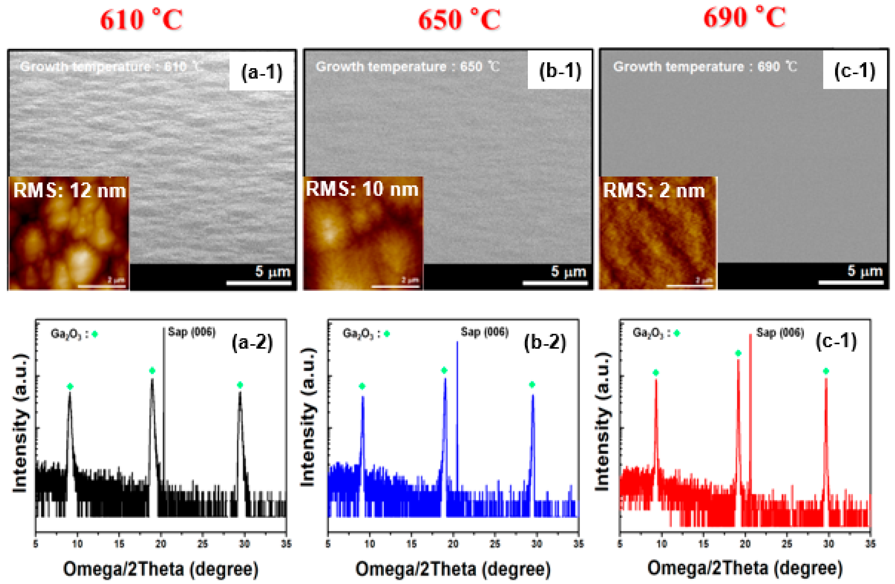
3.1. Growth of κ-Phase Ga2O3 on Sapphire Substrate

The temperature dependent growth study was carried out at a fixed VI/III molar flow ratio, while varying the growth temperature from 610 to 690 °C. A significant improvement in the surface morphology was observed as the growth temperature increased from 610 to 690 °C, evidenced by both top-view SEM and AFM images shown in Figure 1(a-1),(b-1),(c-1). A reduced root-mean-square (RMS) roughness (2 nm) was obtained from the sample grown at 690 °C. In addition, narrower full-width-at-half-maximum (FWHM) values in the XRD peaks were obtained as a higher growth temperature was employed (Figure 1(a-2),(b-2),(c-3)). These XRD peaks were well aligned with the calculated (002), (004) and (006) planes of κ-Ga2O3 peak positions shown in Table 1.

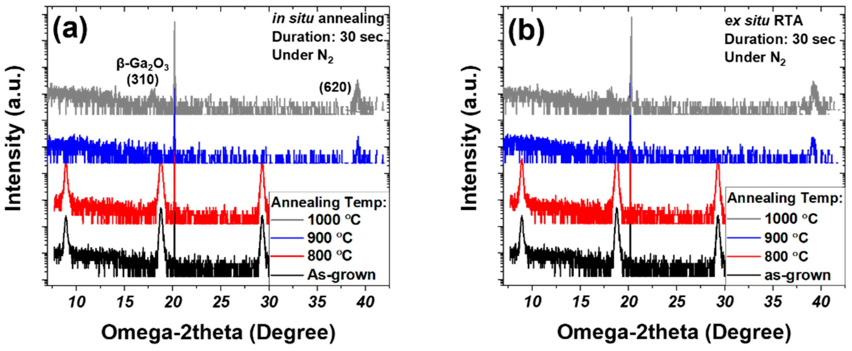
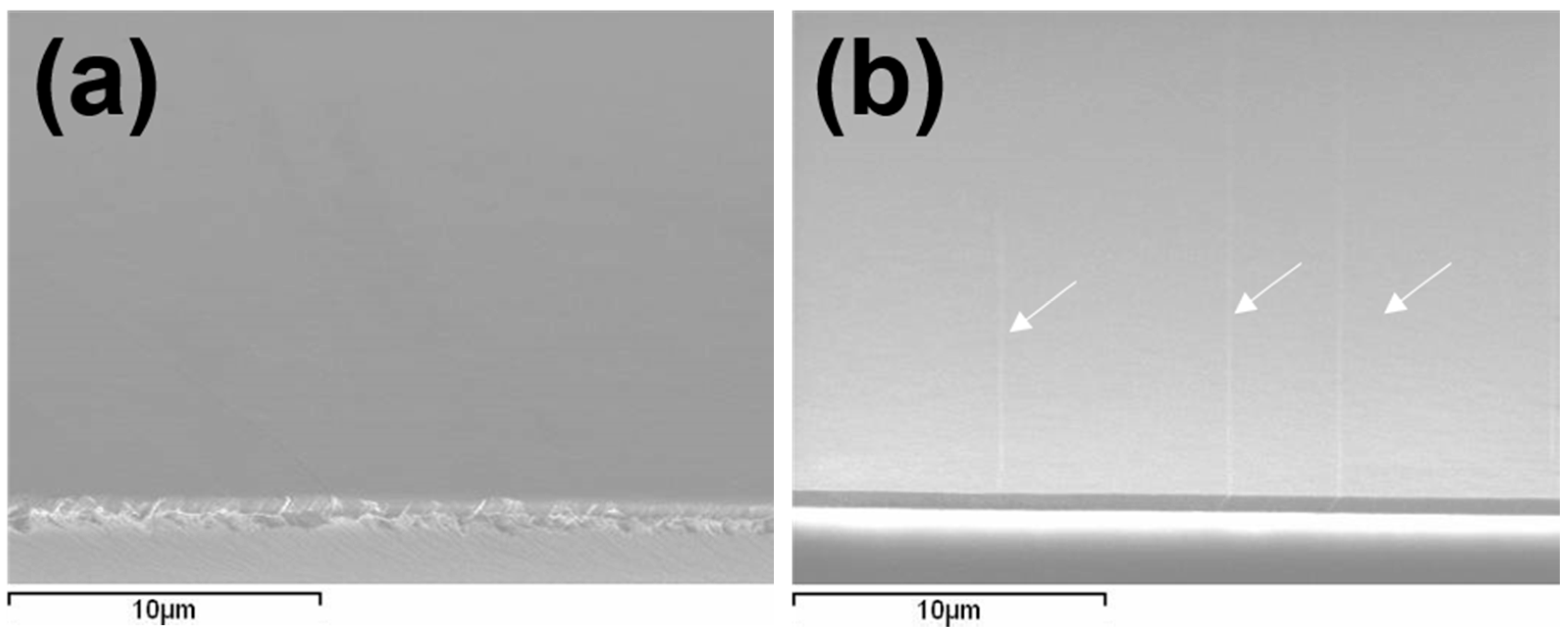
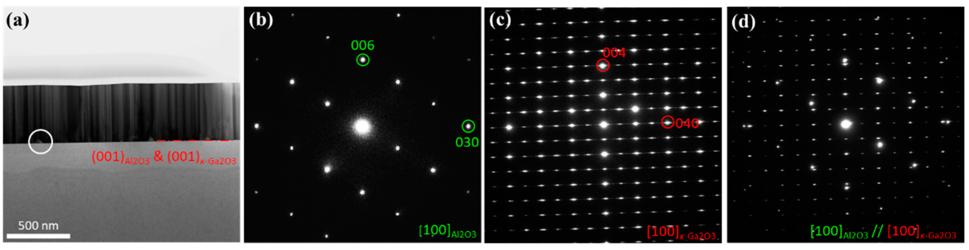
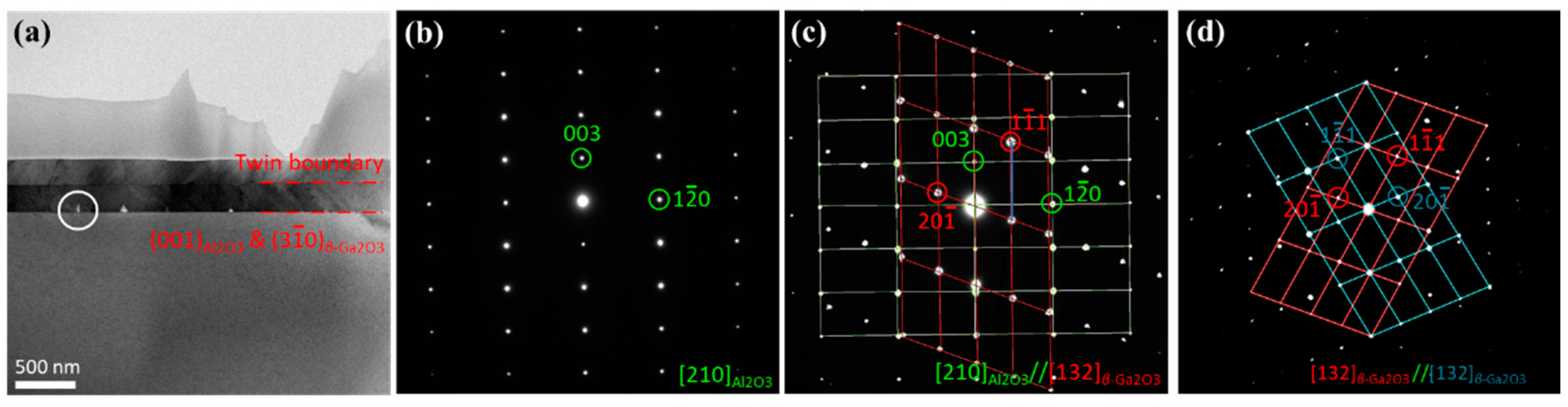
3.2. Effect of Annealing Condition on the Structural Properties

Systematic annealing studies were carried out to investigate the thermal stability of the epitaxial κ-Ga2O3, which was grown at 690 °C. This sample was subjected to annealing at varying temperatures ranging from 800 to 1000 °C under N2 ambience. These annealing conditions are also summarized in Table 2. For in situ annealing, the heating and cooling were performed for 20 min and 10 min, respectively.
Shown in Figure 2a are the XRD patterns for the samples annealed in situ at various temperature for 30 s ranging from 800 to 1000 °C, while those annealed by ex situ RTA are shown in Figure 2b. Regardless of the annealing method, the evidence of phase transition from κ to β phase was not observed from the samples annealed at 800 °C, based on the same observed peak positions, which corresponds to (002), (004), and (006) of orthorhombic κ-Ga2O3.
On the other hand, when the annealing temperature exceeds 900 °C, these peaks disappeared, and new peaks near 19 and 40° started to evolve, which are in close agreement with calculated (310) and (620) planes of monoclinic β-Ga2O3 peak positions, as summarized in Table 3. When the annealing temperature of 1000 °C was employed, the most distinguishable contrast in the intensities of β-Ga2O3 (310) and (620) peaks were observed.
When the annealing temperature of 1000 °C was used, a number of cracks on the surface was observed from annealed sample by RTA, as shown in Figure 3b, while the in situ annealed sample exhibited nearly crack-free surface (Figure 3a). This observation is attributed to a slower heating/cooling rates employed in in situ annealing process, in comparison to those of RTA. This result also suggests that in situ annealing with well-controlled heating and cooling rates will help avoid the generation of severely extended cracks and defects, which can be a problematic issue for the practical device application.
Figure 4a shows an annular bright filed scanning transmission electron microscopy (ABF-STEM) image of the thin film before annealing. The nominal thickness of the Ga2O3 film is around 450 nm. Figure 4b,c show electron diffraction patterns (EDPs) taken from only the Al2O3 substrate and Ga2O3 film, respectively. EDP analysis confirmed the presence of κ phase of Ga2O3, which agrees well to above XRD analyses. Additionally, κ-Ga2O3 phase can keep a good orientation relationship (OR) with the α-Al2O3 matrix, which can be confirmed based on the composite EDPs shown in Figure 4d. This specific orientation relationship (OR) can be described as [100]Al2O3//[100]κ-Ga2O3 and (001)Al2O3//(001)κ-Ga2O3, which is consistent with our previous work [18].
Figure 5a shows an ABF-STEM image of the thin film after annealing. Figure 5b,c EDPs were taken from the α-Al2O3 matrix and composite/interface, respectively. Based on Figure 5c EDPs, it can be shown that the thin film can be indexed as β-Ga2O3 along [132]β-Ga2O3 direction. Additionally, the newly transformed β-Ga2O3 keeps a good OR with matrix as well, which can be described as [210]Al2O3//[132]β-Ga2O3 and (001)Al2O3//(3 1 ¯ 0)β-Ga2O3. Figure 5d EDPs were taken from the β-Ga2O3 thin film only, which can be indexed consistently invoking just the innate twin structure. The twin plan is (3 1 ¯ 0)β-Ga2O3, which is indicated in Figure 5a. Additionally, in Figure 4a and Figure 5a ABF images, there are some holes/gaps along the interface as indicated by the circles. The formation of the hole likely resulted from the large lattice misfit between Ga2O3 and Al2O3, which was reported and discussed in our previous work [18].

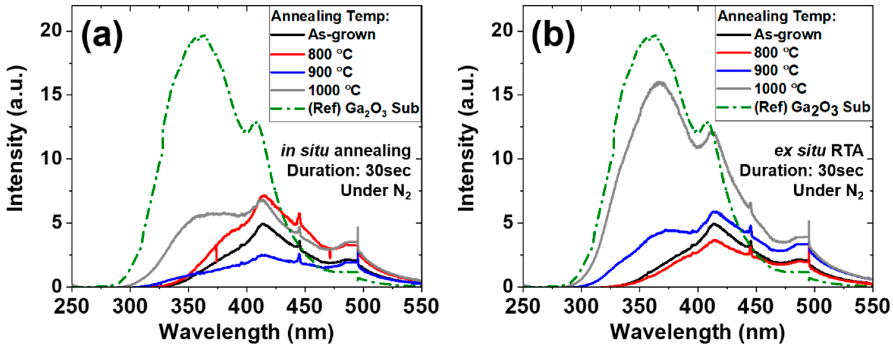
3.3. Effect of Annealing Condition on the Optical and Electrical Properties

Figure 6a shows the photoluminescence (PL) spectra measured from either as-grown or in situ annealed samples, while Figure 6b shows those annealed by RTA. Both as-grown sample and the sample annealed at 800 °C exhibited peak position near 420 nm. On the other hand, as the annealing temperature exceeds 900 °C, another peak near 370 nm started to evolve. A prior study has claimed that the PL peak near 380 nm is related to the transition levels between the oxygen vacancy and unintended N impurities introduced during N2 annealing [19]. On the other hand, the other studies contended the PL peaks near 416, 442, or 464 nm originated from the electron-hole recombination formed by oxygen vacancies or to the recombination of Ga-O vacancy pair [20,21]. While finding the origin of these emissions is a subject of our ongoing study, the comparison between the PL spectrum of (010) Ga2O3 substrate and that of the annealed samples at 1000 °C reveals analogy in their PL spectrum.
Electrical properties of Ga2O3 epitaxial layer before and after annealing were characterized by Van der Pauw Hall measurements. While the as-grown Ga2O3 films were highly resistive, the Ga2O3 layers become conductive when annealed at 1000 °C under N2. N-type conductivity was obtained after the post growth annealing by either in situ or ex situ RTA. The obtained electron concentration was in the range of a few times 10 18   cm 3 with the mobility values ranging from 22 to 43 cm2/V-s, depending on the electron concentrations.

4. Conclusions

High-quality Ga2O3 thin films were grown at 690 °C on sapphire substrate by low-pressure MOCVD using H2 as a carrier gas, TMGa, and H2O as Ga and oxygen precursors. SiH4 was used a doping precursor as well. After material growth, the material was annealed either in situ or ex situ under N2 ambience. Structural, optical, and electrical properties of the grown sample were fully analyzed before and after annealing. A systematic annealing study was performed, which showed that when the annealing temperature was higher than 900 °C, the evidence of phase transition from κ to β phase was observed by XRD and STEM. When in situ annealing was employed, a crack-free surface was obtained. The as-grown sample was highly resistive. After annealing at 1000 °C, this as-grown material became highly conductive with the electron concentration in the range of a few times 10 18   cm 3 and mobilities ranging from 22~43 cm2/V-s. After annealing, the PL spectra of the epitaxially grown Ga2O3 was compared with that of β-Ga2O3 substrate, and a close similarity was observed.

Author Contributions

Data custom: J.L., H.K., L.G., K.H. and X.H.; manuscript: J.L, H.K., X.H., M.R.; review and supervision: M.R. and V.P.D. All authors have read and agreed to the published version of the manuscript.

Funding

This work is supported by Air Force under agreement of FA9550-19-1-0410.

Data Availability Statement

The data presented in this study are available on request from the corresponding author.

Acknowledgments

This work is supported by Air Force under agreement of FA9550-19-1-0410. The authors would like to acknowledge the support and interest of Ali Sayir of USAF-AFMC AFMCAFOSR/RTB) and John Belevins (DCIVUSAF AFMC AFRL/RXME) for providing Ga2O3 substrate. The (S)TEM characterizations made use of the EPIC facility of Northwestern University’s NUANCE Center, which has received support from the SHyNE Resource (NSF ECCS-2025633), the IIN, and Northwestern’s MRSEC program (NSF DMR-1720139).

Conflicts of Interest

The authors declare no conflict of interest.

References

  1. Roy, R.; Hill, V.G.; Osborn, E.F. Polymorphism of Ga2O3 and the system Ga2O3—H2O. J. Am. Chem. Soc. 1952, 74, 719–722. [Google Scholar] [CrossRef]
  2. Razeghi, M.; Park, J.H.; McClintock, R.; Pavlidis, D.; Teherani, F.H.; Rogers, D.J.; Magill, B.A.; Khodaparast, G.A.; Xu, Y.; Wu, J.; et al. A Review of the Growth, Doping, and Applications of β-Ga2O3 Thin Films. Proc. SPIE 2018, 10533, 105330R. [Google Scholar]
  3. Anhar Uddin Bhuiyan, A.F.M.; Feng, Z.; Johnson, J.M.; Huang, H.L.; Hwang, J.; Zhao, H. MOCVD Epitaxy of Ultrawide Bandgap β-(AlxGa1–x)2O3 with High-Al Composition on (100) β-Ga2O3 Substrates. Cryst. Growth Des. 2020, 20, 6722–6730. [Google Scholar] [CrossRef]
  4. Hatipoglu, I.; Mukhopadhyay, P.; Alema, F.; Sakthivel, T.S.; Seal, S.; Osinsky, A.; Schoenfeld, W.V. Tuning the responsivity of monoclinic solar-blind photodetectors grown by metal organic chemical vapor deposition. J. Phys. D Appl. Phys. 2020, 53, 454001. [Google Scholar] [CrossRef]
  5. Bi, X.; Wu, Z.; Huang, Y.; Tang, W. Stabilization and enhanced energy gap by Mg doping in ε-phase Ga2O3 thin films. AIP Adv. 2018, 8, 025008. [Google Scholar] [CrossRef] [Green Version]
  6. Teherani, F.H.; Rogers, D.J.; Sandana, V.E.; Bove, P.; Ton-That, C.; Lem, L.L.C.; Chikoidze, E.; Neumann-Spallart, M.; Dumont, Y.; Huynh, T.; et al. Investigations on the substrate dependence of the properties in nominally-undoped beta-Ga2O3 thin films grown by PLD. Proc. SPIE 2017, 10105, 101051R. [Google Scholar]
  7. Shinohara, D.; Fujita, S. Heteroepitaxy of corundum-structured α-Ga2O3 thin films on α-Al2O3 substrates by ultrasonic mist chemical vapor deposition. Jpn. J. Appl. Phys. 2008, 47, 7311. [Google Scholar] [CrossRef]
  8. Kawaharamura, T.; Dang, G.T.; Furuta, M. Successful growth of conductive highly crystalline Sn-doped α-Ga2O3 thin films by fine-channel mist chemical vapor deposition. Jpn. J. Appl. Phys. 2012, 51, 040207. [Google Scholar]
  9. Sasaki, K.; Higashiwaki, M.; Kuramata, A.; Masui, T.; Yamakoshi, S. MBE grown Ga2O3 and its power device applications. J. Cryst. Growth 2013, 378, 591–595. [Google Scholar] [CrossRef]
  10. Sasaki, K.; Higashiwaki, M.; Kuramata, A.; Masui, T.; Yamakoshi, S. Growth temperature dependences of structural and electrical properties of Ga2O3 epitaxial films grown on β-Ga2O3 (010) substrates by molecular beam epitaxy. J. Cryst. Growth 2014, 392, 30–33. [Google Scholar] [CrossRef]
  11. Zhang, F.B.; Saito, K.; Tanaka, T.; Nishio, M.; Guo, Q.X. Structural and optical properties of Ga2O3 films on sapphire substrates by pulsed laser deposition. J. Cryst. Growth 2014, 387, 96–100. [Google Scholar] [CrossRef]
  12. Yao, Y.; Okur, S.; Lyle, L.A.; Tompa, G.S.; Salagaj, T.; Sbrockey, N.; Davis, R.F.; Porter, L.M. Growth and characterization of α-, β-, and ϵ-phases of Ga2O3 using MOCVD and HVPE techniques. Mater. Res. Lett. 2018, 6, 268–275. [Google Scholar] [CrossRef] [Green Version]
  13. Murakami, H.; Nomura, K.; Goto, K.; Sasaki, K.; Kawara, K.; Thieu, Q.T.; Togashi, R.; Kumagai, Y.; Higashiwaki, M.; Kuramata, A.; et al. Homoepitaxial growth of β-Ga2O3 layers by halide vapor phase epitaxy. Appl. Phys. Express 2014, 8, 015503. [Google Scholar] [CrossRef]
  14. Park, J.H.; McClintock, R.; Razeghi, M. Ga2O3 metal-oxide-semiconductor field effect transistors on sapphire substrate by MOCVD. Semicond. Sci. Technol. 2019, 34, 08LT01. [Google Scholar] [CrossRef]
  15. Boschi, F.; Bosi, M.; Berzina, T.; Buffagni, E.; Ferrari, C.; Fornari, R. Hetero-epitaxy of ε-Ga2O3 layers by MOCVD and ALD. J. Cryst. Growth 2016, 443, 25–30. [Google Scholar] [CrossRef]
  16. McClintock, R.; Jaud, A.; Gautam, L.; Razeghi, M. Solar-blind photodetectors based on Ga2O3 and III-nitrides. Proc. SPIE 2020, 11288, 1128803. [Google Scholar]
  17. Sun, H.; Li, K.H.; Castanedo, C.T.; Okur, S.; Tompa, G.S.; Salagaj, T.; Lopatin, S.; Genovese, A.; Li, X. HCl flow-induced phase change of α-, β-, and ε-Ga2O3 films grown by MOCVD. Cryst. Growth Des. 2018, 18, 2370–2376. [Google Scholar] [CrossRef]
  18. Xu, Y.; Park, J.H.; Yao, Z.; Wolverton, C.; Razeghi, M.; Wu, J.; Dravid, V.P. Strain-Induced Metastable Phase Stabilization in Ga2O3 Thin Films. ACS Appl. Mater. Interfaces 2019, 11, 5536–5543. [Google Scholar] [CrossRef]
  19. Liu, L.L.; Li, M.K.; Yu, D.Q.; Zhang, J.; Zhang, H.; Qian, C.; Yang, Z. Fabrication and characteristics of N-doped β-Ga2O3 nanowires. Appl. Phys. A 2010, 98, 831–835. [Google Scholar] [CrossRef]
  20. Binet, L.; Gourier, D. Origin of the blue luminescence of β-Ga2O3. J. Phys. Chem. Solids 1998, 59, 1241–1249. [Google Scholar] [CrossRef]
  21. Chang, K.W.; Wu, J.J. Low-Temperature Growth of Well-Aligned β-Ga2O3 Nanowires from a Single-Source Organometallic Precursor. Adv. Mater. 2004, 16, 545–549. [Google Scholar] [CrossRef]
Figure 1. [Top- (a-1), (b-1), (c-1)] Top-view SEM images showing the surface morphologies of the film grown at 610, 650, and 690 °C where inset figures show the corresponding 5   μ m × 5   μ m atomic force microscopy (AFM) images with measured root-mean-square roughness (RMS); [bottom- (a-2), (b-2), (c-2)] corresponding HR-XRD spectra from the samples grown at 610, 650, and 690 °C.
Photonics 08 00017 g001
Figure 2. (a) XRD patterns taken from the samples subjected to varying in situ annealing temperature; (b) XRD patterns taken from the samples subjected to varying ex situ RTA temperature.
Photonics 08 00017 g002
Figure 3. (a) Angled-view SEM image showing crack-free surface after in situ annealing at 1000 °C for 30 s and (b) angled-view SEM image showing the presence of extended cracks after ex situ RTA at 1000 °C for 30 s where cracks are indicated as white arrows.
Photonics 08 00017 g003
Figure 4. (a) Annular bright field (ABF) image showing the general structural feature of the thin film before annealing. Electron diffraction patterns (EDPs) of (b) Al2O3 substrate along [100] zone-axis and (c) κ-Ga2O3 along [100] zone-axis. (d) Composite EDPs of [100]Al2O3 and [100]κ-Ga2O3 taken from the interface. Circled area in (a) indicates the hole along the interface.
Photonics 08 00017 g004
Figure 5. (a) ABF image showing the general structural feature of the thin film after annealing. (b) EDPs of Al2O3 substrate along [210] zone-axis. (c) Composite EDPs of [210]Al2O3 and [132]β-Ga2O3 taken from the interface. (d) EDPs of the twins within the β-Ga2O3 (ad) were obtained from the thin films after annealing. Circled area in (a) indicates the hole along the interface.
Photonics 08 00017 g005
Figure 6. (a) PL spectra of the as grown sample and the samples in situ annealed at various temperatures; (b) PL spectra of the as grown sample and the samples annealed by ex situ RTA at various temperatures. The PL spectrum from (010) Ga2O3 substrate is also plotted as a reference.
Photonics 08 00017 g006
Table 1. Summary of measured and calculated reflection angle from the Ga2O3 grown at 690 °C on c-plane sapphire substrate (lattice parameter of orthorhombic κ-Ga2O3: a = 5.12 Å, b = 8.78 Å, c = 9.4 Å).
Phase(h k l)d-Spacing
(Å)
Calculated Bragg’s AngleMeasured Peak Position
κ-Ga2O3 (Orthorhombic)(002)4.7059.4°9.6°
κ-Ga2O3 (Orthorhombic)(004)2.35319.1°19.4°
κ-Ga2O3 (Orthorhombic)(006)1.56829.4°29.96°
Table 2. The annealing condition to investigate the effect of annealing temperature for the sample grown at 690 °C.
Annealing Temp.
[°C]
Annealing TypeAmbienceDuration
(s)
800in situ annealingN230
800ex situ RTAN230
900in situ annealingN230
900ex situ RTAN230
1000in situ annealingN230
1000ex situ RTAN230
Table 3. Summary of measured and calculated reflection angle from the annealed Ga2O3 grown on c-plane sapphire substrate (lattice parameter of monoclinic β-Ga2O3: a = 12.23 Å, b = 3.04 Å, c = 5.8 Å, and β = 103.7°).
Phase(h k l)d-Spacing
(Å)
Calculated Bragg’s AngleMeasured Peak Position
β-Ga2O3
(Monoclinic)
(310)2.41218.6°18.5°
β-Ga2O3
(Monoclinic)
(620)1.20639.7°39.5°
Publisher’s Note: MDPI stays neutral with regard to jurisdictional claims in published maps and institutional affiliations.

