Reflectivity of Cholesteric Liquid Crystals with an Anisotropic Defect Layer Inside


Department of Automation, Biomechanics and Mechatronics, Lodz University of Technology, 90-924 Lodz, Poland
*
Author to whom correspondence should be addressed.
Photonics 2020, 7(3), 58; https://doi.org/10.3390/photonics7030058
Submission received: 15 June 2020
/
Revised: 27 July 2020
/
Accepted: 7 August 2020
/
Published: 10 August 2020
(This article belongs to the Special Issue Advances in 3OM: Opto-Mechatronics, Opto-Mechanics, and Optical Metrology)
Abstract
:In this study, first, we numerically investigated the reflectivity of a cholesteric liquid crystal with an anisotropic defect layer inside. To model optical phenomena in the examined system, a 4 × 4 matrix method was employed. The tests were carried out for different thicknesses of the whole system, different thicknesses of the defect layer, as well as different defect layer locations inside the cell. Next, a cholesteric liquid crystal comprising a defect layer and held between two parallel electrical conductors was also considered. In this case, the optical properties of the system could also be adjusted by an external applied electric field. Some interesting simulation results of the reflection coefficient (i.e., the fraction of electromagnetic energy reflected) were obtained, illustrated, and discussed. The simulation results showed a significant influence of both the defect and the external electric field on the selective reflection phenomenon, and the possibility of controlling the shape of the reflection spectrum. Finally, some potential applications of the analyzed optical system were discussed.
1. Introduction
Photonic crystals consisting of artificial or organic self-organizing periodic structures have opened up new possible applications in modern electronic devices. Some of the possible practical applications of such materials in different branches of science and technology can be found, for instance, in recent review papers [1,2,3,4,5]. Especially attractive is the use of cholesteric liquid crystals (CLCs) since the macroscopic properties of such optical structures can be manipulated by external stimuli.
CLCs are organic materials with unique and useful optical properties. They are composed of optically anisotropic and uniaxial elements (molecules), with one major and two minor principal axes, which are also mutually perpendicular locally. In cholesteric liquid crystals, there is a long-range orientational order of the elongated molecules with locally preferred common direction called the director. Whereas in nematic liquid crystals, the elastic forces and torques tend to establish a uniform orientation of the director, the chiral molecules in CLCs lead in equilibrium to a helical arrangement with the director perpendicular to the helix axis [6]. This way, they have a one-dimensional periodic modulation of dielectric constants, which leads to interesting optical effects.
Owing to the optical anisotropy and helical twist, CLCs are characterized by the so-called selective reflection. It means that for the light incident along the helical axis (normal incidence), the circularly polarized light with the same handedness as that of CLC, is totally reflected in the specific wavelength range. The edges of this bandwidth are defined by two sharp optical modes which correspond to circularly polarized standing waves in which the electric field in the bulk of the sample is aligned along either the ordinary or the extraordinary molecular axes [7]. This unique feature of the selective reflection is widely used in numerous applications such as reflective displays, tunable color filters, or mirrorless lasers [8].
In isotropic periodic media, defects have been created by the removal or addition of a material, or by an alteration of the refractive index of one or a number of elements of photonic crystals [9]. In the anisotropic optical structures considered in this study, defects can be introduced by replacing a part of the host medium with a material that has a different dielectric constant and can make defect modes in the forbidden bands [10]. The defect makes such structures more useful (such as doped semiconductors) and can be successfully used for constructing narrowband filters [11,12,13], low threshold lasers [14,15], and other optical devices. A broad overview of the properties of all currently existing defective modes in CLCs, including both the proposed theoretical approaches and the performed experimental observations, can be found in monography [16]. In particular, efficient applications of localized modes for low-threshold lasing at the frequencies of localized modes are presented in this study as the most recent achievements in this area.
Generally, two ways to introduce a defect in CLCs have been proposed (and discussed in more detail below): either by replacing a thin layer of the CLC with an isotropic material [10], or by introducing a phase jump in the cholesteric helix [7]. In the first case, in analogy with isotropic periodic structures, a defect can be produced in a helical structure by adding an isotropic layer in the middle of a CLC. In the second case, a chiral twist defect can be created by rotating one part of the sample about its helical axis without separating the two parts.
Yang et al. [10] theoretically studied the reflection and transmission of light from a one-dimensional system consisting of two layers of cholesteric liquid crystal sandwiching a thin layer of the isotropic medium as a defect. Reflection spectra for normal incidence, calculated by using the so-called “faster Berreman method”, were studied to obtain the wavelengths and intensities of defect modes when the refractive index and the thickness of the defect layer were varied.
Gevorgyan and Harutyunyan [17] considered some properties of defect modes in chiral photonic crystals with an anisotropic defect layer. They solved the problem by the Ambartsumian’s layer addition method previously developed for the solution of astrophysical problems of multiple scattering in turbid media, and further extended to optical wave propagation through inhomogeneous media [18]. As a result, the influence of the defect layer thickness variation and its location in the chiral photonic crystal on defect mode properties were investigated. However, the amplitudes of the reflected and transmitted fields related to the incident wave were expressed by using 2 × 2 Jones matrix method, in which both the effect of refraction and multiple reflections between plate interfaces (dielectric discontinuities) are neglected [19].
Kopp and Genack [7] considered photonic properties of a defect created by twisting one part of an anisotropic structure relative to the rest of the sample. The authors restricted their discussion to samples with a chiral twist of 90° in the center of the sample, which creates a photonic defect at a frequency in the center of the stopband. However, varying the chiral twist angle in the range 0–180° tunes the defect frequency from the low to the high-frequency band edge. The study demonstrated that twisting one part of a chiral photonic structure about its helical axis creates a single circularly polarized localized mode that gives rise to an anomalous crossover in propagation. This is in contrast to a defect in a binary layered medium that produces two orthogonally polarized degenerate localized modes.
In another study, Schmidtke et al. [13] used two layers of a highly cross-linked CLC polymer film to create a phase jump of 90° in the cholesteric structure. They observed experimentally enhanced fluorescence inside the photonic stopband and laser emission due to a photonic defect mode in a dye-doped cholesteric polymer network. The observed emission peak can be attributed to the localized defect mode generated by the phase jump of the cholesteric helix and it agrees with the simulation results of Kopp and Genack [7], who have theoretically predicted the presence of a defect mode in the center of the stopband.
In the study [20], the twist defect mode inducted by a discontinuity of the director rotation around the helix axis at an interface of two photopolymerized cholesteric liquid crystal layers has been experimentally demonstrated in the transmission spectrum. The existing self-organized helical structure of such composite film acts as a one-dimensional photonic crystal. Finally, the authors observed optically pumped laser action based on the twist defect mode.
Ha et al. [21] considered quasi-periodic Fibonaccian phase defects in single-pitched cholesteric liquid crystalline systems. Fundamental optical properties were discussed as functions of phase jump (orientational defect angles), unit lengths, and the orders of Fibonacci systems. The performed simulations of reflection spectra demonstrated simultaneous red, green, and blue reflections or multiple photonic bandgaps, and the color of reflections could be controlled by an orientational defect angle.
Motivated by the literature review presented above, in this study, we considered a defect in the form of an anisotropic layer with different thicknesses, different locations of the defect layer inside the analyzed CLC cell, as well as different total thicknesses of the investigated system. To model optical phenomena, we implemented the 4 × 4 matrix method which gives accurate numerical results and was used in many previous papers [9,20,21,22,23,24,25,26,27,28,29,30,31]. On the contrary to numerous former studies examining the defect modes in nondeformed CLCs, we also investigated the influence of an external electric field applied to the considered CLC optical system with a defect layer inside. This is important from a technological point of view since the investigated optical system can also be additionally tuned during operation by altering the director field of the CLC.
The study is organized as follows. Section 2 presents the considered optical system, i.e., CLC cell with a defect layer inside, sandwiched between two homogenous and isotropic conducting glass samples. Section 3 shortly summarizes the most essential steps in the computational method of the director field of the CLC deformed by an externally applied electric field and the 4 × 4 matrix calculation method. Some interesting numerical simulations of the reflectance obtained for different configurations of the system, different values of the parameters, as well as different director fields of the CLC are reported and discussed in Section 4. Lastly, a brief summary and the conclusions of the study are outlined in Section 5.
2. Model of the Considered Optical System
Generally, in a liquid crystal cell under a given boundary condition and an externally applied field, the liquid crystal is in the director field configuration that minimizes the total free energy of this system [32]. In other words, there is a critical amplitude of the electric field below which the internal elastic strength of the liquid crystal exceeds the electric forces; therefore, the system remains undeformed from its base state. When a relatively large external electric field is applied to the cell, the liquid crystal will reorient because of the dielectric interaction between the crystal and the applied field. This bifurcation field-induced reorientation of the liquid crystal is referred to as the Fréedericksz transition [32].
Generally, determining the director field in a cholesteric liquid crystal device is complicated due to the large number of material parameters that characterize it. The tendency of the director to take on a particular spatial distribution can be understood in terms of the well-known elastic continuum theory. For instance, in papers [33,34,35], the problem of the continuum theory for nematic and cholesteric liquid crystals is exhaustively reported, and, therefore, it is not considered in detail in this study. According to this theory, elastic forces arising from the molecular structure of the material resist any distortion to the director field from its equilibrium state. Such distortions can arise for a number of reasons, including interaction with external electric/magnetic fields, coupling with the material flow of the liquid, or from interactions with confining surfaces [36]. When subjected to competing influences, the director will adjust throughout the sample and, as a result, must be treated as both space- and time-dependent function.
In our analysis, we considered situations, where the electric field interacts with the liquid crystal deformation. In the case of positive dielectric anisotropy of the CLCs, the molecules tend to align parallel to the electric field if voltage (electric field) is applied across the cell. As boundary conditions, we assumed the strong anchoring of the molecules of the CLC at surfaces of substrates and the deformation of the CLC characterized by the so-called tilt angle and twist angle of the molecules, which depends on the applied electric field, the anisotropy of the electrical permittivity of the liquid crystal, and the anisotropy of the elastic stiffness of the liquid crystal. The anisotropic defect layer is manifested by a locally constant director in the area of the defect layer.
Motivated by the structure of the simplest electro-optic devices, also in our system, a thin layer of a cholesteric liquid crystal is sandwiched between two plates (substrates) which are treated in a way which leads to the surface interaction imposing a specified orientation on the liquid crystal (boundary conditions of the director field). The optical properties of the investigated system can be additionally adjusted by applying an external electric field whose distorting influence on the CLC opposes that of the surfaces.
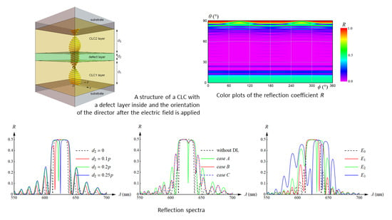
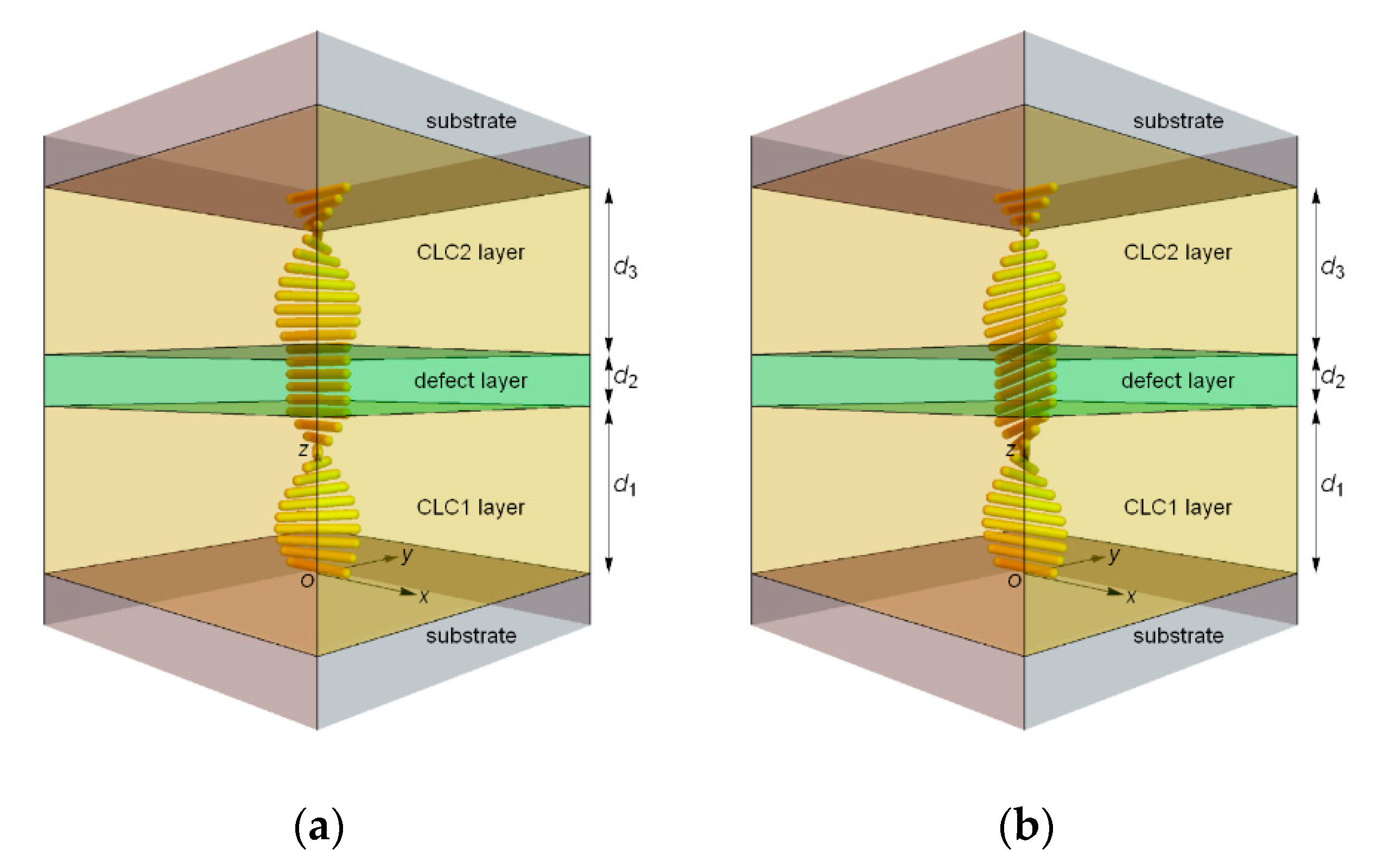
Figure 1 presents two configurations of the structure of the modeled optical system, i.e., CLC cell with a defect layer (DL) inside, and sandwiched between two (lower and upper substrates) homogenous isotropic media. Figure 1a presents the nondeformed director field, whereas Figure 1b shows the deformed director field caused by the applied electric field. The studied system is located in the right-handed Cartesian coordinate system, where the z-axis was chosen to be the twist axis of the CLC.
The considered system can be treated as a multilayer system CLC1-DL-CLC2 with thicknesses of d1, d2, and d3, respectively. In all considered cases, the whole CLC cell with the total thickness D = d1 + d2 + d3 was divided into N equal multiple elementary layers (sliced into a large number of slabs) of the thickness 1 nm, which was parallel to the substrates (i.e., xy plane). Each imaginary elementary n-th layer can be treated as a homogenous layer with the same orientation of the optical axis, characterized by two angles, i.e., tilt angle and twist angle. The tilt angle was measured from the z-axis to the direction of the optical axis of the molecule, while the twist angle was measured from the x-axis to the projection of the optical axis of the molecule on the xy plane. As a result, each elementary layer can be treated locally as an anisotropic homogenous medium. The spatial period of the helical structure of the CLC characterized by the pitch p can be easily varied by adding dopants and changing temperature. The ordinary and extraordinary refractive indices were no = 1.4639 and ne = 1.5133, respectively, whereas the pitch of the right-handed periodic helical structure was p = 420 nm. These values corresponded to the CLC cholesteryl-nonanoate–cholesteryl-chloride–cholesterylacetate (20:15:6) composition at the temperature 298 K [37]. As a result, the light with right circular polarization and normally incident onto a single CLC layer had a bandwidth in the range of λ ~ (615–635) nm, whereas the light with the left circular polarization did not have any. The considered system was surrounded by the optical media with the refraction index ns on its both sides, equal to ns = 1.4 (the value that corresponds to glass medium). We assumed that both CLC and DL were not absorbing, and the values of the parameters ns, no, and ne did not depend on the wavelength of the incident light.
The incident light propagated in the lower substrate (n = 0), then in the CLC1, DL, and CLC2 (n = 1, 2, …, N), and finally in the upper substrate (n = N + 1). The optical axis of the molecules of cholesteric liquid crystals laid on the xy plane which was parallel to the substrates and changed periodically along the z-direction. The orientation of the wave vector of the oblique incident nonpolarized beam of monochromatic light with wavelength λ in the lower substrate was represented by angles θ and ϕ. The angle θ was measured from the z-axis to the direction of the wave vector of the incident beam of light, while the angle ϕ was measured from the x-axis to the projection of the director of the wave vector of the incident beam of light on the xy plane [38,39].
3. Calculation Methods
We considered a cholesteric liquid crystal confined between parallel plates at z = 0 and z = D and subject to strong planar anchoring at these surfaces as boundary conditions. We applied electric potential between the plates giving rise to an electric field parallel to the z-axis. We took into account the liquid crystal with positive electric anisotropy; therefore, the director tended to align parallel to the local electric field, and at the same time, the director was in competition with the direction of the strong planar anchoring. The deformation of the director occurred in two planes, in which it was possible to describe the director by two angles, namely the abovementioned tilt angle θc (measured from the z-axis to the direction of the optical axis of the molecule), and the twist angle ϕc (measured from the x-axis to the projection of the optical axis of the molecule on the xy plane).
For our calculations, the equations governing the static behavior of the liquid crystal with the variables θc and ϕc of the director field could be obtained from the equations expressing conservation of momentum, angular momentum, and Maxwell equations for the electric displacement field, with the appropriate boundary conditions that reflected the assumption of strong planar anchoring and that the voltage dropped across the considered cell was equal to the applied voltage. The solution of these equations in the nondimensional form depended on nondimensional parameters, i.e., the nondimensional elastic anisotropy, the nondimensional electric anisotropy, and the nondimensional applied voltage. In turn, the abovementioned nondimensional parameters depended on a large number of material parameters that characterized the investigated system. However, from the point of view of the optical properties of the system, such as reflectivity or transmissivity, the spatial distribution of the director had fundamental importance. Therefore, in our research, during the analysis of the considered optical cell in an external electric field, we took into account directly different distributions of the director field that corresponded to different amplitudes E of the applied electric field. In this way, the obtained results were more general and they could be directly adopted to systems with different material properties, both mechanical and optical.
To model optical phenomena in the analyzed system, we used the 4 × 4 matrix method implemented based on the mathematical formalism presented in [40]. More detailed information regarding the realized computer algorithm of the applied computation technique was presented in detail in one of our previous papers [39]. Below, only the main stages of this method are listed:
- Entering values of all required parameters of the considered optical system, i.e., ns, no, ne, d1, d2, d3, p, λ, θ, and ϕ;
- Calculation of the dielectric tensors ε(n) of the substrates (n = 0 and n = N + 1) and the dielectric tensors ε(n) of the individual elementary crystal/defect layers (n = 1, 2, …, N);
- Calculation of the wave vectors kσ(n) of all four elementary waves (σ = 1, 2, 3, 4) in all elementary layers based on the wave equation;
- Computation of the optical polarization vectors pσ(n) of the individual elementary waves representing the directions of the electric field as well as the corresponding vectors qσ(n) of the magnetic field;
- Computation of the 4 × 4 transition matrix, which describes the relationships between amplitudes As, Ap of the electric field of the incident waves, amplitudes Bs, Bp of the electric field of the reflected waves, and amplitudes Cs, Cp of the electric field of the transmitted waves, both for s and p waves, respectively;
- Calculation of the reflection coefficient R (the fraction of the electromagnetic energy reflected) or optionally the transmission coefficient T (the fraction of the electromagnetic energy transmitted) of the incident light.
This mathematical approach is an effective technique in describing the optical properties of multi-layered structures and has been widely employed by many researchers in numerous problems, including the investigation of liquid crystal displays [41], the propagation of electromagnetic waves in stratified bianisotropic chiral structures [42], the study of various uniaxial, biaxial dielectric, magnetic materials [43,44], the investigation of the effect of stress-induced anisotropy on localized mode in photonic crystal [31], and the study of different kinds of cells of CLC lasers [45].
4. Results and Discussion
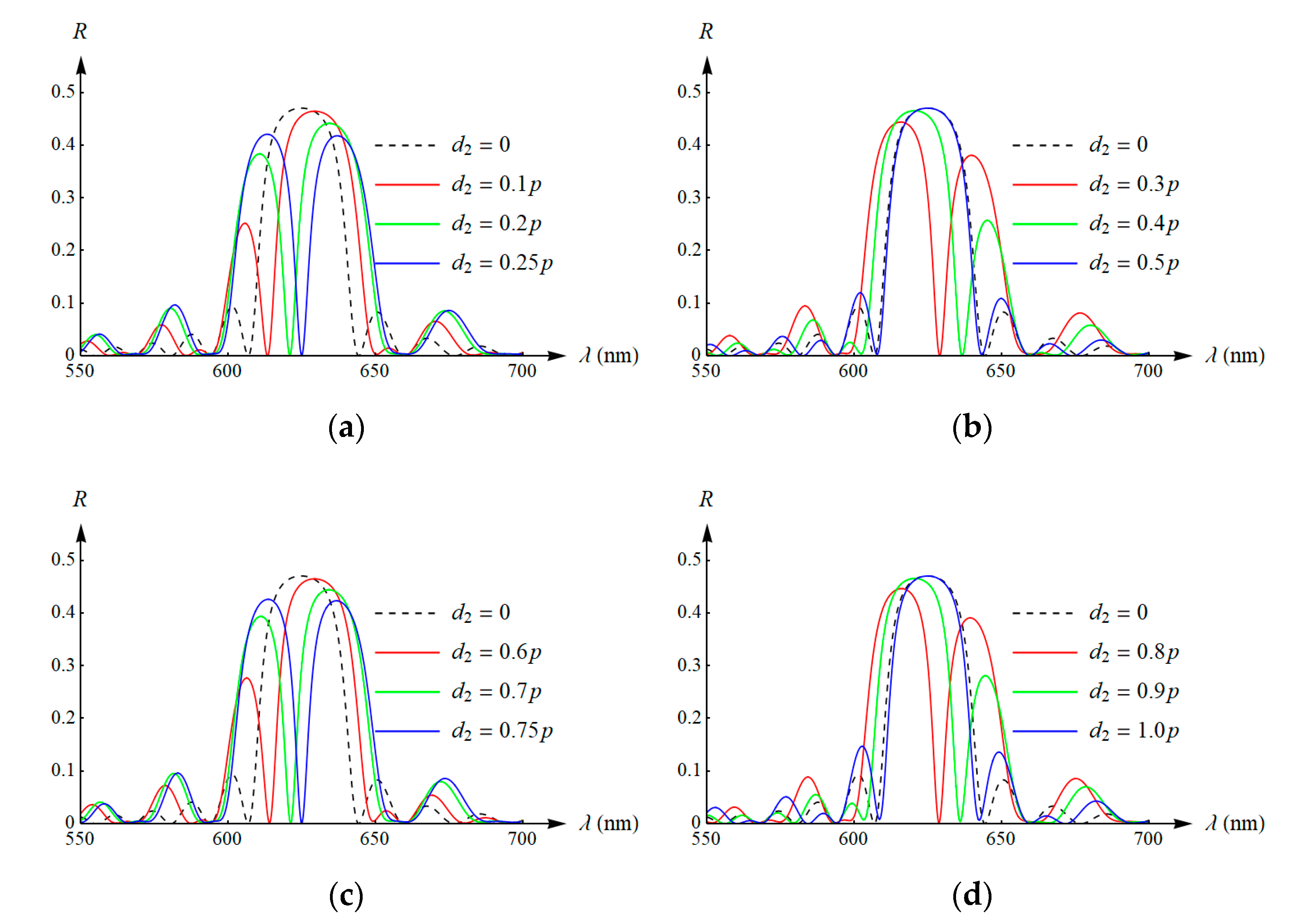
First, we examined the optical system for d1 = d3 = 10 p (further referred to as model 1) and for different values of the thickness d2. In this case, the defect layer was located in the center of the studied cell. A beam of a monochromatic nonpolarized light was incident normally on the surface of the investigated optical system, i.e., perpendicular to the xy plane. For the sake of completeness and to increase the transparency of the obtained results, the results were presented in a few charts together with the curve obtained for the ideal system as a reference, i.e., without the defect layer (plotted by the dashed curve). The presented simulation results show that the thickness of the defect layer had a significant impact on the shape of the simulated spectral curves, especially in the band of the selective reflection. As one can see, visible dips in the spectral curves were induced by the introduction of the defect layer. Moreover, if the defect layer thickness was changed, the defect mode bandwidth of the incident light was changed too. Generally, the defect effect was present near the center and these curves had a certain asymmetry. However, for some values of the defect layer thickness, this effect was exactly in the center of the bandwidth and the spectral curves were symmetric. It should be noted that a similar effect can also be obtained in another way. For instance, a peak in transmission was observed in the middle of the bandgap, when a system with a spacerless defect was created in sculptured thin films by rotation of the substrate by an additional 90° in the middle of the film fabrication process [12].
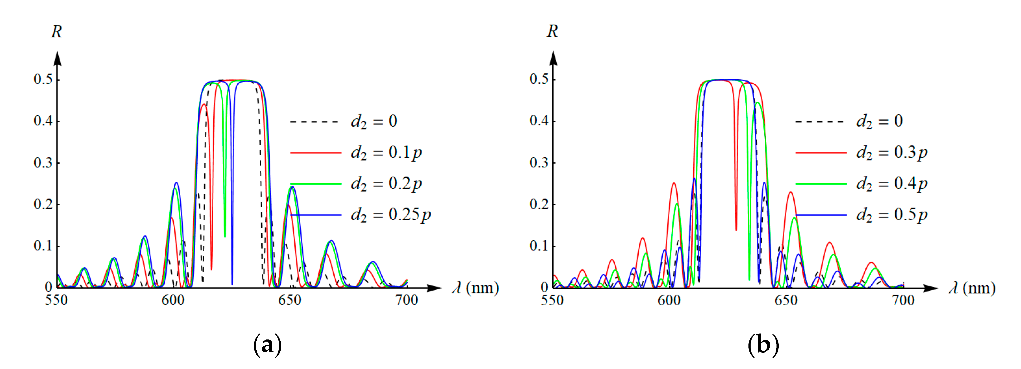
The regularities in spectra presented in Figure 2 are easy to understand. When the thickness of the defect increased, the characteristic peak of the maximum value shifted toward the long-wave boundary of the bandwidth, while the second maximum appeared simultaneously on the left side of the spectral curve. For the layer thickness equal to 0.25 p (Figure 2a), the spectral curve had a form of two symmetrical maxima with a slightly smaller amplitude around the wavelength of the maximum reflection for the system without the defect. With a further increase in the thickness of the defect (see Figure 2b), a similar situation occurred, but on the other side of the band gap (i.e., mirror image in comparison to the results presented in Figure 2a). For d2 = 0.5 p, the obtained spectral curve was almost identical to the curve obtained for the system without the defect (only a very small narrowing of the selective reflection bandwidth was visible). Increasing the defect thickness from 0.5 p to p (see Figure 2c,d) caused a similar effect to changing the value of the d2 parameter in the range from 0 to 0.5 p (compare these curves with the curves presented in Figure 2a,b, respectively).
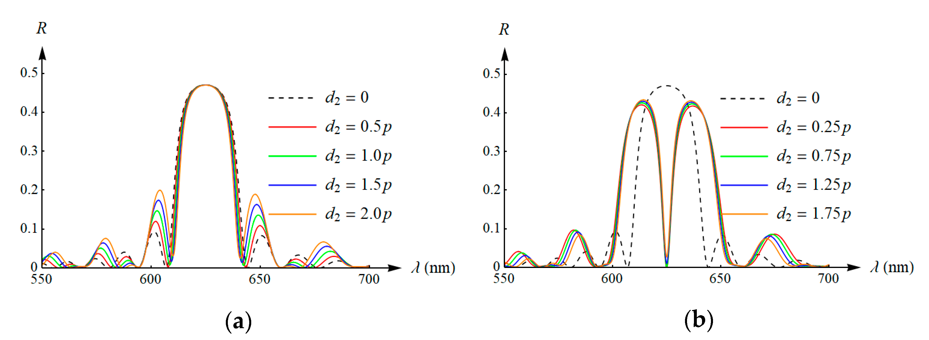
Figure 3a shows a comparison of curves obtained for the defect layer thickness of 0.5 p, p, 1.5 p, and 2 p, while Figure 3b shows the comparison for d2 = 0.25 p, 0.75 p, 1.25 p, and 1.75 p, respectively. In the first case (Figure 3a), we obtained similar results to for the system without the defect layer. The increase in the thickness of the defect layer (i.e., d2 equal to 0.5 p, p, 1.5 p, or 2 p) caused only a very small and gradual narrowing of the bandwidth and a significant increase in the amplitude of the side peaks. In turn, for the value of the parameter d2 tested in Figure 3b (i.e., d2 equal to 0.25 p, 0.75 p, 1.25 p, and 1.75 p), two symmetrical peaks were obtained with a slightly smaller amplitude and with a zero reflection coefficient for λ = (no + ne)·p/2 ≈ 625 nm. This gradual increase in the defect thickness resulted in a gradual but slight flattening of these spectral curves.
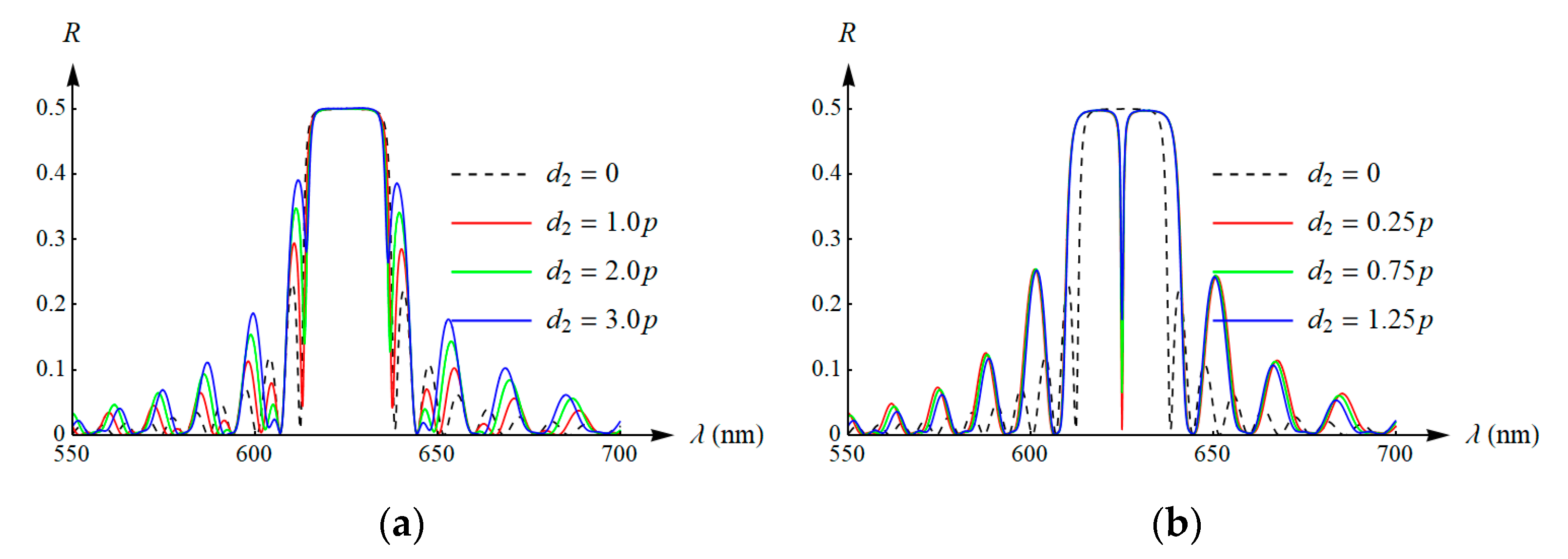
Figure 4 and Figure 5 show curves similar to those seen in Figure 2 and Figure 3, but for the optical system with d1 = d3 = 20 p and different values of the thickness d2 (further referred to as model 2). Through the analysis of the results of numerical simulations for the considered model 2, one can come to the same conclusions as for model 1. However, for greater values of the total thickness of the considered system, the observed selective reflection phenomenon was more pronounced. In the case of model 1, we observed a significant expansion of the selective reflection bandwidth (two adjacent peaks), with the simultaneous reduction in the average amplitude of the reflection coefficient. On the other hand, for model 2, the bandwidth extension was slightly smaller, but there was no significant reduction in the reflection coefficient in the bandwidth. This effect resulted from a larger value of the total twist angle of the liquid crystal optical axis, due to which the interference effects inside the crystal was stronger, and the selective reflection coefficient was greater.
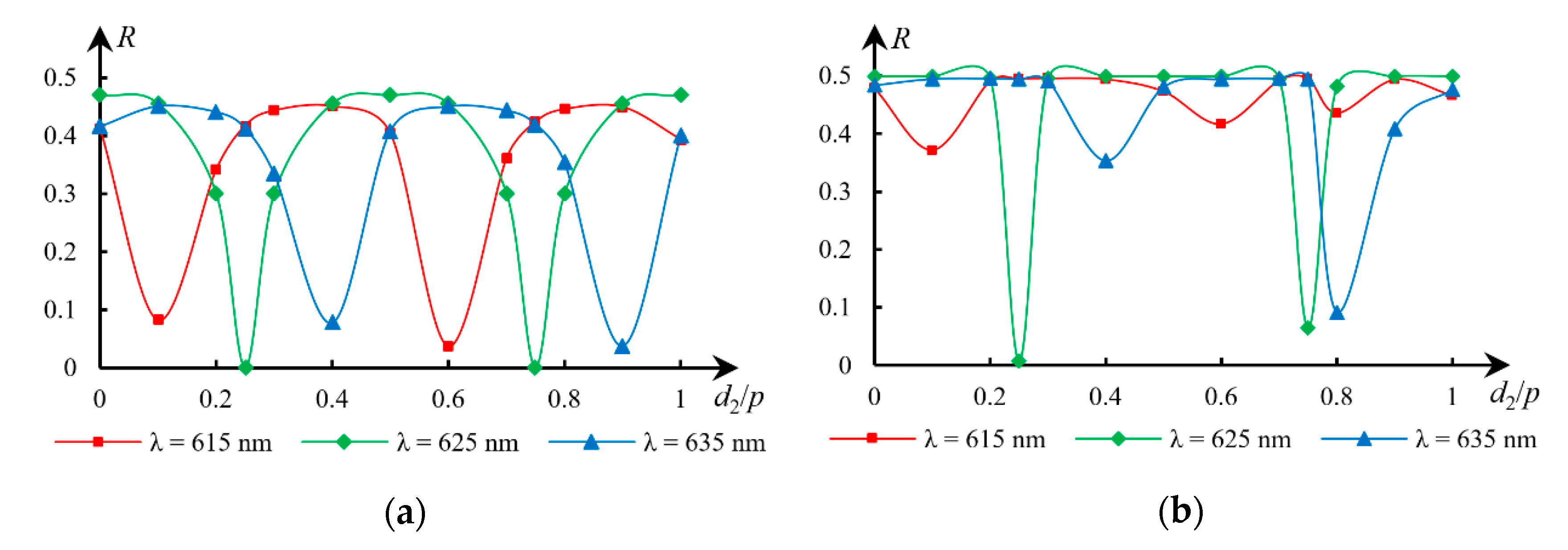
It is known that in the case of CLCs without defects, the value of the reflection coefficient is almost the same within the entire forbidden band λ in the range (nop, nep). Figure 6 shows the relationship between the reflection coefficient for the wavelength λ = (no + ne)·p/2 ≈ 625 nm and the thickness of the defect layer, for both model 1 and model 2. In addition, we also presented similar curves obtained for other wavelengths, i.e., λ = no∙p ≈ 615 nm and λ = ne·p ≈ 635 nm.
The simulation results presented in Figure 6 show that the reflection coefficient for individual wavelengths varied significantly depending on the thickness of the defect layer (in the range from 0 to 0.5), which was already observed in previous figures. Figure 6a shows that for the wavelength of 625 nm, the total reflection occurred for d2 = 0, 0.5 p and p, while no reflection occurred for d2 = 0.25 p and 0.75 p. Similar changes occurred for other wavelengths, i.e., 615 and 635 nm, with their maximum and minimum values occurring for other thicknesses of the defect layer. More interesting results are presented in Figure 6b. They were obtained for a greater total thickness of the investigated optical system. In addition, in this case, for the wavelength 625 nm and d2 = 0.25 p, there was practically complete quenching of the selective reflection. However, for d2 = 0.75 p, the value of the reflection coefficient no longer reached zero. This effect, also for larger values of the d2 parameter (i.e., d2 = 1.25 p), is clearly visible in Figure 5b. As the value of the thickness d2 increased, the values of the reflection coefficient for λ = 615 and λ = 635 nm also increased. As a result, it can be stated that for the thicker tested optical system and thicker defect layers, the selective reflection bandwidth was significantly broadened without an undesired decrease in its amplitude.
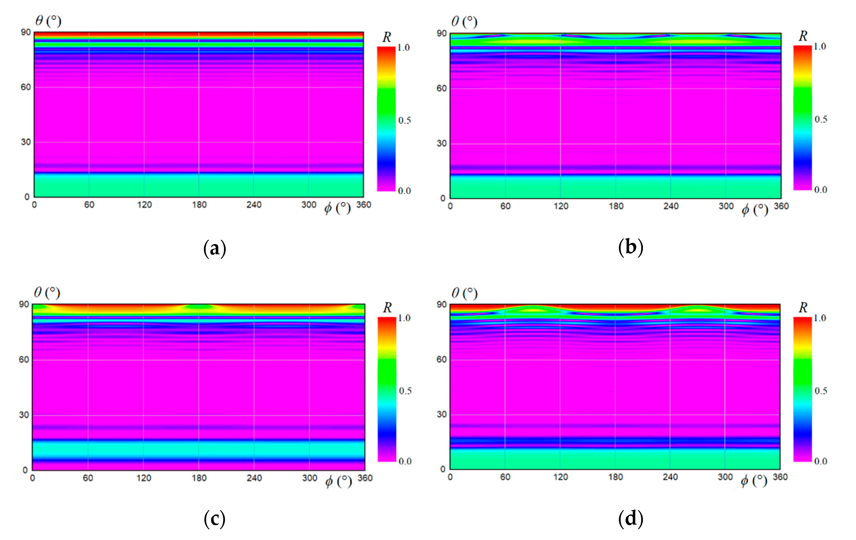
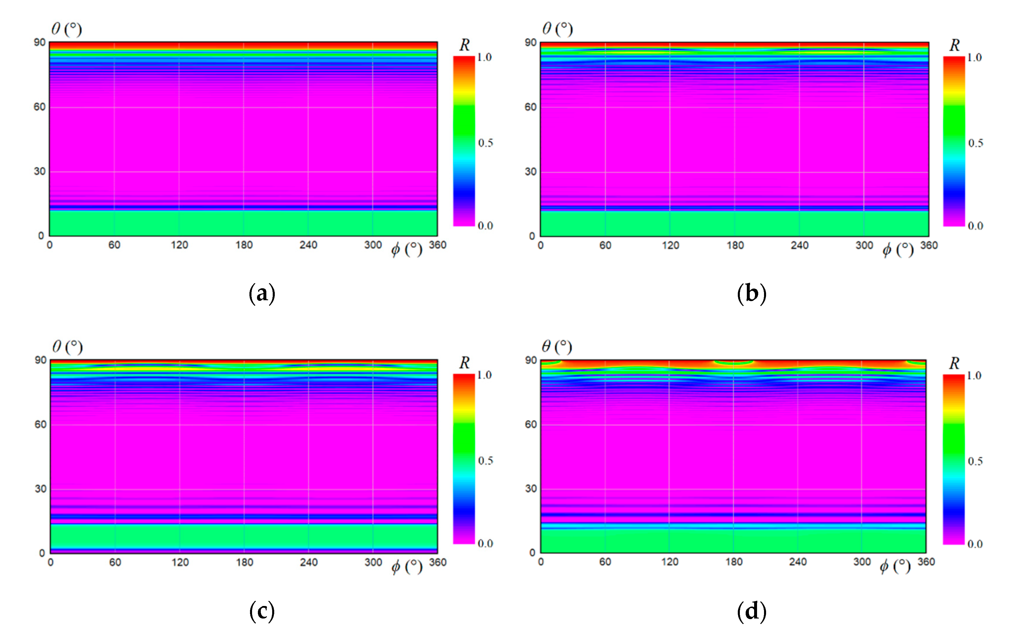
As it has been already noted, the abovementioned numerical tests were obtained for normal incidence of light. However, in our research, we also considered the oblique direction of the incident light. The direction of the beam of obliquely incident light can be described by two angles (θ and ϕ), and it was presented in detail in our previous papers [38,39]. Figure 7 presents color plots of the reflection coefficient R for the light with the wavelength λ = 625 nm incident onto model 1 and for different values of the thickness d2, whereas Figure 8 shows similar plots computed for model 2. Numerical simulations presented in Figure 7 and Figure 8 show that the reflection coefficient practically did not change when the angle ϕ changed (especially for thicker layers of the investigated system (see Figure 8), while the distribution of the reflection coefficient changes when the θ angle changes. However, for the θ angle close to zero (almost perpendicular incidence of light), the reflection coefficient was practically constant. Significant changes could be observed only for large values of the θ angle, i.e., around 80–90°.
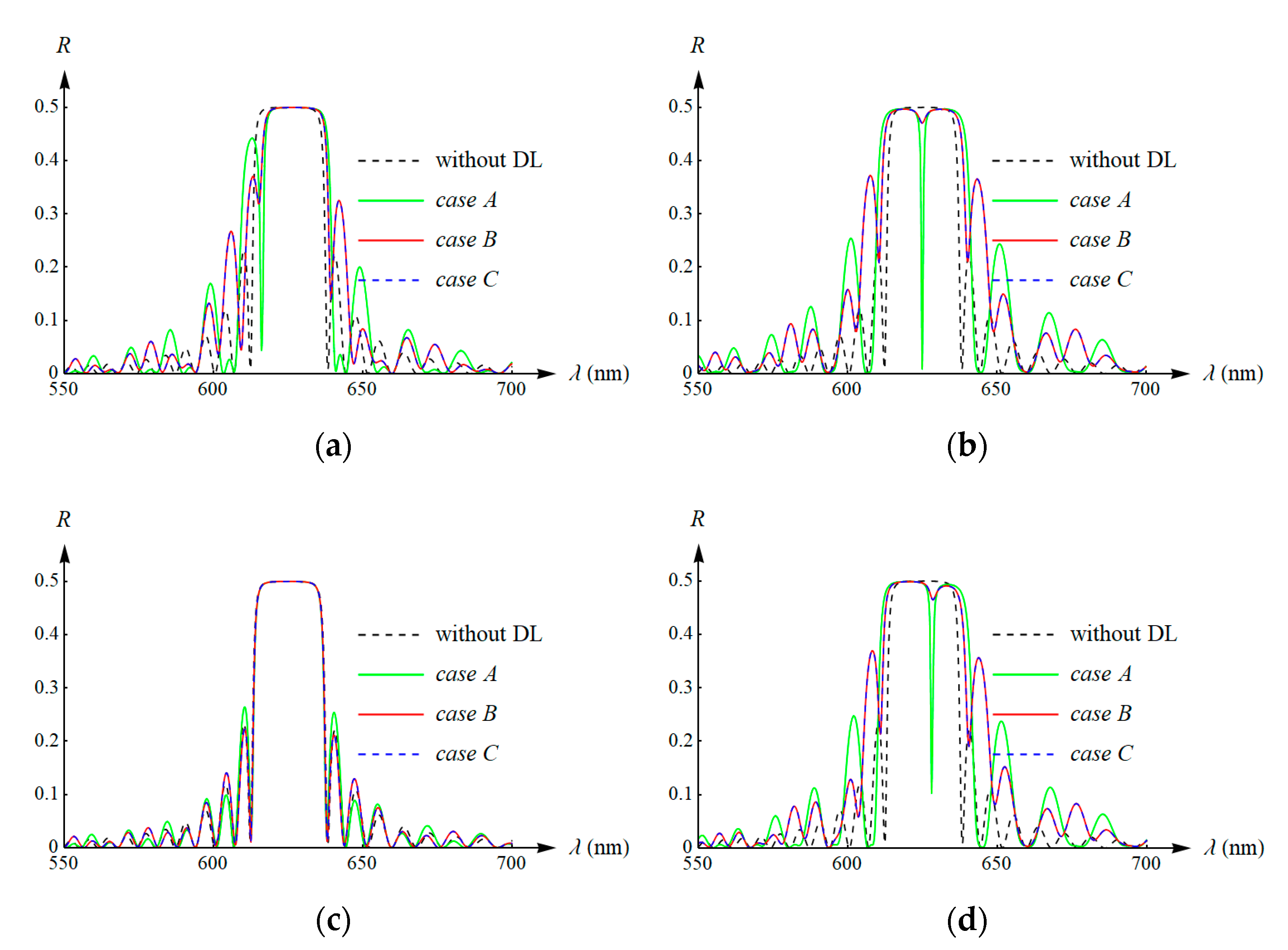
The above figures present the simulations obtained for symmetrical systems (d1 = d3). Here we also examined the influence of the location of the defect layer inside the investigated CLC cell. To do it, we compared previously tested model 2 (i.e., d1 = d3 = 20 p, further referred to as case A), with two examples of the asymmetrical location of the defect layer, namely d1 = 10 p, d3 = 30 p (further referred to as case B) and d1 = 30 p, d3 = 10 p (further referred as case C). Again, we considered the case of normal incidence of light first. For comparison, the presented figures also show the case where there was no defect layer (marked as “without DL”). The analysis of the results presented in Figure 9 leads to the conclusion that in asymmetrical systems (i.e., case B and case C), the spectral curves differed slightly from the curves obtained for the symmetrical system (case A). In addition, the influence of the defect location in the reflection spectra for case B and case C was practically unobservable. Namely, we did not find a significant difference in spectral characteristics between case B and case C.
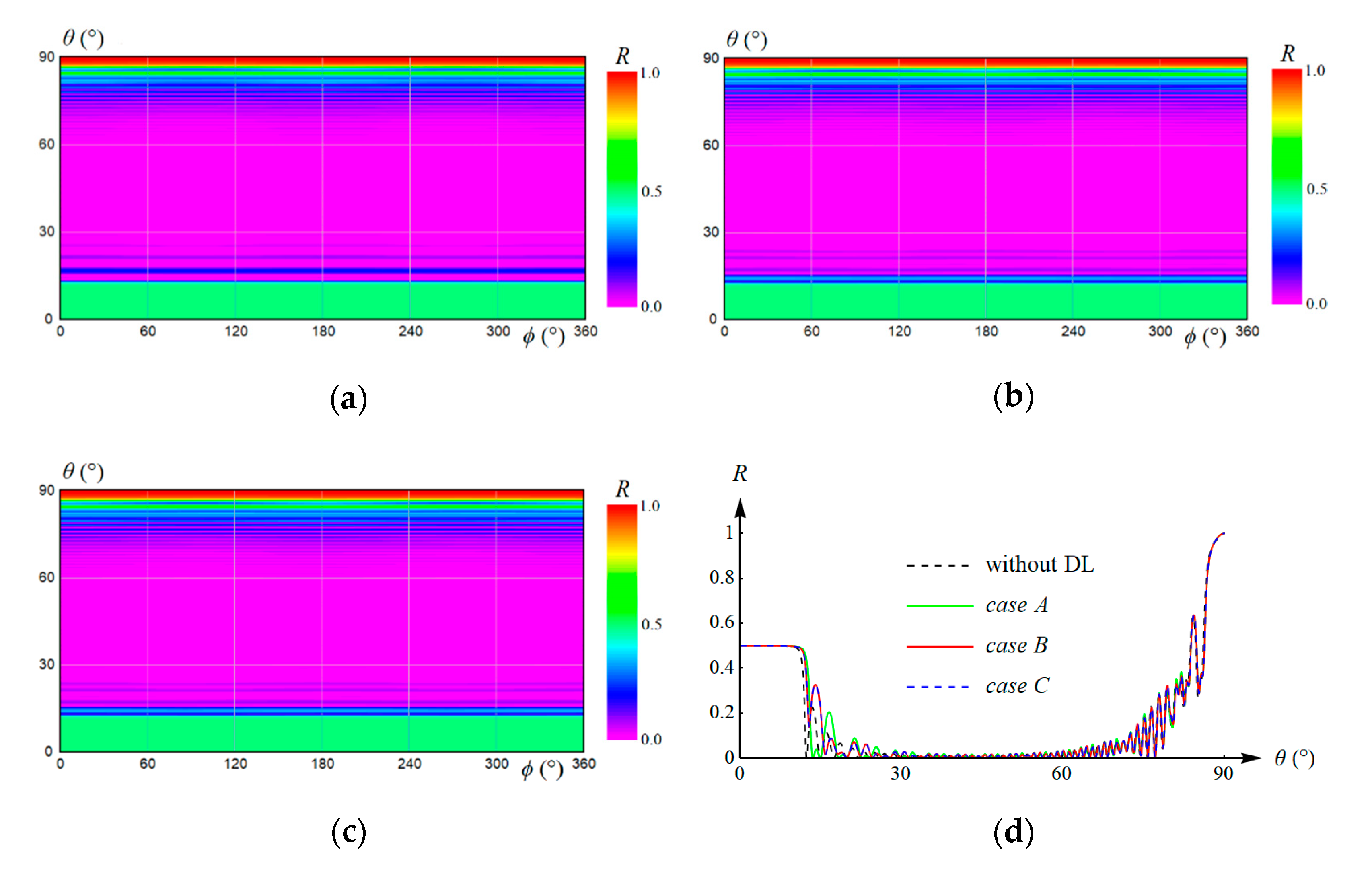
We also calculated the reflectance distribution (color plots) for the oblique incident light for all three cases (i.e., case A, case B, and case C). Color plots presenting these calculations in a graphical form are depicted in Figure 10. The presented results (here calculated for d2 = 0.1 p) confirmed the previous conclusions obtained on the basis of spectral curves and distributions of the reflection coefficient. Practically, no differences in the reflection spectra were observed for case B and case C, which is clearly shown in Figure 10d.
At the end of our research, we analyzed our optical system with a deformed director distribution caused by an externally applied electric field. As it was mentioned in Section 3, from the point of view of the optical properties of the examined system, the spatial distribution of the director field is fundamentally important. Therefore, in the present study, we directly took into account the different director distributions that corresponded to different amplitudes E of the electric field, without considering material parameters of the examined system. This approach was sufficient for the planned qualitative analysis.
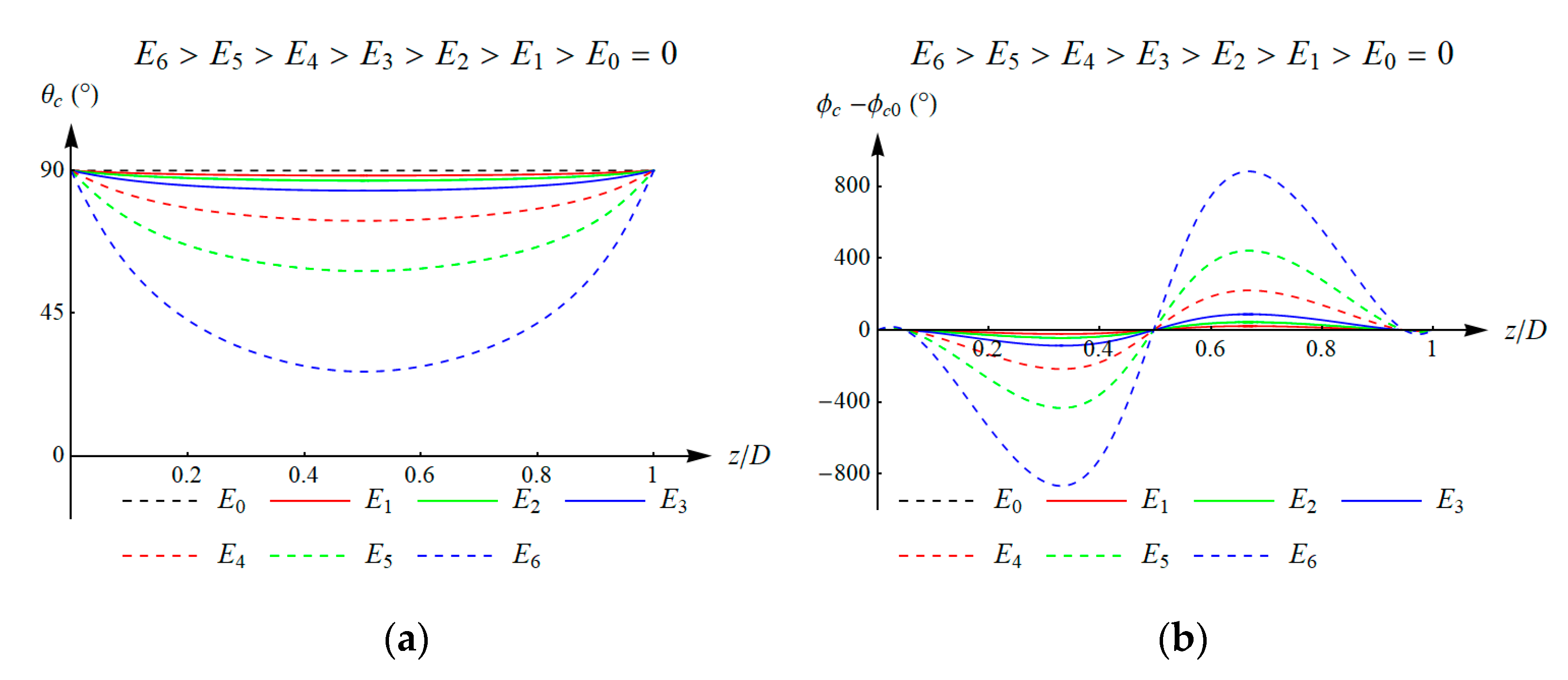
Figure 11 presents the applied distributions of the director characterized by the tilt and twist angles as functions of the coordinate z. For better clarity of the presented results, Figure 11b shows the relative deformations of the angle, i.e., ϕc–ϕc0, in relation to the angle ϕc0 obtained for the case of the undeformed director field. The presented curves correspond to different values of the amplitude E of the applied electric field, where the following relation was preserved: E6 > E5 > E4 > E3 > E2 > E1 > E0 = 0. To increase the transparency of the obtained curves representing the director field, the results were presented together with the curve obtained for the undeformed director field as a reference, i.e., for the electric field E0 = 0 (plotted by the dashed black curve). As it can be seen, the curves obtained for E1, E2, and E3 were characterized by a relatively low director field deformation, while the curves obtained for E4, E5, and E6 were characterized by a relatively large director field deformation. Therefore, the electric fields with the amplitudes E1, E2, and E3 can be regarded as low electric fields, whereas electric fields with the amplitudes E4, E5, and E6 can be regarded as high electric fields.
For further analysis, we considered only the optical system marked as model 2. Figure 12, Figure 13 and Figure 14 show the spectral reflectance curves obtained for normal incidence of light, when the director field was deformed by an electric field with different amplitudes. The results shown in Figure 12 were obtained for the system without a defect layer (d2 = 0), and the results depicted in Figure 13 were obtained for d2 = 0.25 p, whereas Figure 14 presents the results calculated for d2 = 0.5 p. Moreover, Figure 12a, Figure 13a, and Figure 14a correspond to the director field deformations obtained for the low electric field (E1, E2, and E3), while Figure 12b, Figure 13b, and Figure 14b correspond to the director field deformations obtained for the high electric field (E4, E5, and E6). The same results as those depicted in Figure 12, Figure 13 and Figure 14 are shown again in Figure 15. However, Figure 15 directly shows the influence of different values of the thickness of the defect layer for a fixed director field, i.e., under the given electric field.
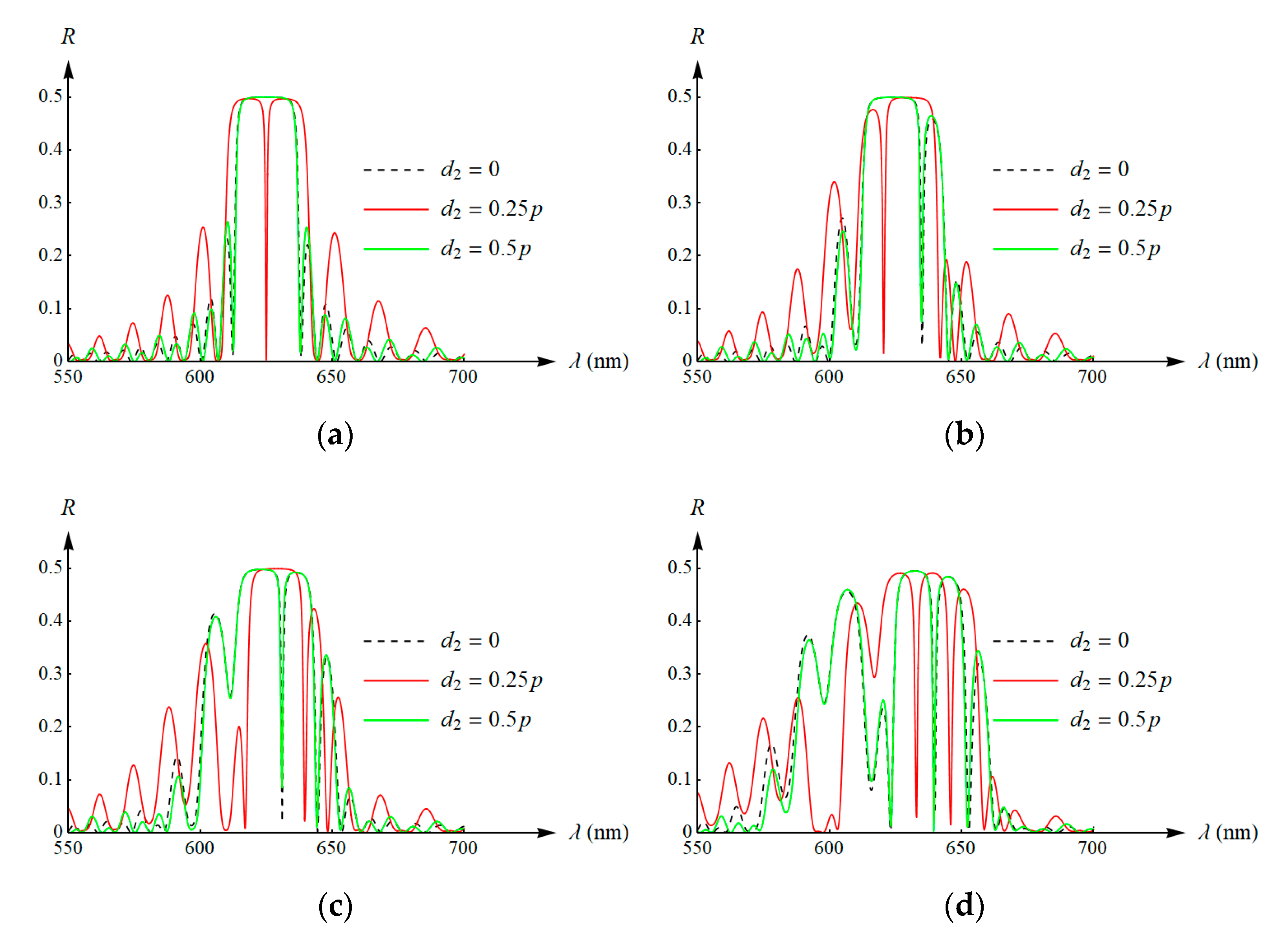
In the case of the system without a defect layer, the application of a relatively low electric field caused a dip in the spectral curve near the right edge of the bandgap (see Figure 12a). With the increase in the amplitude of the electric field, the existing dip became more visible and shifted toward the short-wave boundary of the bandwidth. As a result, the applied electric field gave a similar effect to the introduction of a defect layer in the case of an undeformed director field of the CLC. What is more, the position of this dip can be precisely tuned within the range of the bandgap that exists for the undeformed director field. Similar conclusions can also be outlined when considering the results presented in Figure 14a that correspond to the system with a defect layer equal to 0.5 p. For the system with the defect layer thickness equal to 0.25 p, a dip in the spectral curve occurred in each presented case (see Figure 13a). For an undeformed director field, this dip was observed in the middle of the bandgap. The application of a low external electric field changed the position of this dip within the bandgap. It is worth noting that the shift of this dip can be both in the direction of the long-wave and the short-wave boundary of the bandwidth, depending on the amplitude of the applied electric field. The observation allowed the change in position of this narrow range. For example, this property can be useful when it is necessary to compensate the position of the dip due to the appearance of undesired external stimuli, such as mechanical or thermal stresses, acting on the considered system. In turn, the analysis of the results presented in Figure 12b, Figure 13b, Figure 14b clearly shows that in a high electric field applied to the tested system with or without a defect layer, the system lost the properties of the selective reflection and the defect modes. Finally, the analysis of the results presented in Figure 15 led to similar conclusions. In particular, for a fixed value of the electric field, the spectral curves were similar for both the system with no defect and the half-wavelength defect layer. In turn, the spectral curves obtained for the quarter-wavelength defect layer differed significantly from the spectral curves obtained for the system without the defect and with the half-wavelength defect layer, even if the applied electric field had the same value.
The results of the present research may be of significant practical importance, since the considered model of the optical system is often found in engineering applications. Namely, in real engineering applications, CLCs are usually sandwiched between two parallel substrates coated with transparent conductive electrode, and voltage is applied across the cell. The applications of such systems can be greatly extended if the reflection can be electrically adjusted. This problem was considered in previous papers. As an example, Yang et al. [46] developed a (polymer network/nematic liquid crystal/chiral dopant) composite exhibiting the bandwidth of the selective reflection spectrum, which is wider and narrower reversibly with increasing and decreasing temperature, respectively. Lu and Chien [47] reported a method of fabricating single-layer color cholesteric liquid crystal displays from a polymer-stabilized cholesteric liquid crystal, where the reflective wavelength can be electrically switched to reflect blue or green from a cell initially reflecting the red color. Bailey et al. [48] investigated the electrical tuning of negative dielectric anisotropy cholesteric liquid crystals under the influence of AC and DC electric fields. They showed an electric effect with potential applications in tunable optical filters, optical pressure/stress sensors, or tunable lasers. In recent years, the application of polymer stabilization in CLCs provides a new dimension to achieve color tuning (for instance, see paper [8] and references cited therein). In the abovementioned paper [8], the authors experimentally investigated the broadening of the reflection band caused by an external electric field applied to the CLC cell. They studied a variety of factors affecting the reflection band broadening of polymer stabilized cholesteric liquid crystals, including the effect of moisture, the effect of alignment layer thickness, the effect of ionic additives, the relation between reflection band broadening and impedance, and the influence of morphology of the polymer network. As a result, by controlling these factors, they observed a wide reflection band to cover the entire visible region under low voltages.
The simulation results presented above concern the analysis of the CLC cell with a defect layer inside and a director field deformed by an external applied electric field. In these studies, we assumed that the spatial director’s field distribution could be easily changed by an electric field. In general, studying the dynamic behavior of the considered cholesteric structures in an electric field is not an easy task, and some theoretical aspects in this area can be found in paper [6]. It should also be emphasized that the theoretical stability analysis of the orientation pattern of cholesteric liquid crystals both in electric and magnetic fields has been considered for a few decades. For instance, the unstable behavior of the planar texture between two conducting glass samples at voltages much below those needed to unwind the cholesteric helix was noticed [49]. More intensively, the problem of obtaining a stable and homogeneous uniform lying helix structure has been reported since the late eighties. However, most recently, the developed cholesteric liquid crystal device with the uniform lying helix structure shows stable and reversible characteristics with a short time response [50]. As a result, this enabled the solving of the long-standing problem of stability and hysteresis particularly to meet the manufacturing requirements dedicated to engineering applications.
The presented simulations regarding the appearance of similar defect modes agree with the related theoretical, numerical, or experimental results presented in the literature [51,52], where amplitudes and spectral positions can be elastically tuned. Moreover, our research leads to analogical conclusions as in other references, where it has been demonstrated that the amplitude, the number, and the position of the optical defect modes induced in the bandwidth depend on the thickness, the refractive index, and the anisotropy of the defect layer [17,53,54,55,56,57]. The proposed combination of the study of the defect modes caused by the defect layer inside and the tuning of the optical properties of the system by means of an electric field extends the existing research found in the literature and increases the possibility of its potential real applications.
5. Conclusions
First, we investigated the influence of an existing defect in the form of an anisotropic layer sandwiched by CLC. Numerical tests were carried out for different thicknesses of the system, different thicknesses of the defect layer, and different locations of this defect inside the investigated cell. In addition, we also studied the influence of an external electric field applied to the considered optical system that is important from a viewpoint of the technological aspects. Some interesting numerical simulations were obtained, illustrated, and discussed. The results were presented in the form of the reflection spectra for the normal incidence of light or color planar distributions of the reflection coefficient calculated for the oblique incident light. We showed that a defect layer placed inside CLC has a significant influence on the selective reflection phenomenon, and both the shape and the bandwidth of the spectral curve can be tuned by a dopant defect layer. In particular, the results obtained for model 2 showed that defect modes can have an extremely narrow spectral width (narrow dip in the reflection spectrum or narrow peak in the transmission spectrum) on the order of a few Å.
The considered optical system serves as a model for more complex and realistic cholesteric liquid crystal devices. The obtained numerical results give a new insight into the behavior of practical devices based on the CLC with defect layers and additionally tuned by the external electric field. The analysis presented here demonstrates that there is a significant benefit for the industry to be gained from applying similar methods to models of liquid crystals in more general settings.
The research presented in this paper reflects current issues related to the new approach of modern optics, in which optical properties are determined by geometric factors, including dopants. An example of such a successful implementation is the investigated CLC cell with a defect inside. For instance, such a defect layer with a controlled anisotropy can be created by introducing a layer of a nematic liquid crystal, in which the orientation of the optical axis can be controlled electrically. In other cases, the thickness of the defect layer can be adjusted by the change of the applied voltage. This anisotropic defect provides an additional degree of freedom for tuning the defect modes. As a result, the analyzed CLC with a defect layer can work as an optical diode, which transmits light in one direction and prevents its propagation in the opposite direction. Currently, such research goals seem justified in engineering due to the expected conversion of electric signals to optical ones.
When it comes to using an external electric field in the considered system, the simplest operating regime is to switch between two states by the sudden application or removal of an electric field. In this way, in the absence of an external electric field, the analyzed system shows a selective reflection, including defect modes resulting from the existing defect layers. By means of small changes in the electric field, it is possible to precisely tune the optical properties of the system, which gives a similar effect to introducing defect layers with different thicknesses. In turn, the application of a high electric field causes the abovementioned optical properties to vanish.
In conclusion, in many technological applications, active tuning and switching of defect modes is desired. By introducing defect layers and applying an external electric field, the propagation of light can be precisely controlled through tailoring of the periodic dielectric structure of the CLC.
Author Contributions
Conceptualization, D.G. and J.A.; methodology and software, D.G.; investigation, validation and formal fnalysis, D.G. and J.A.; writing—original draft preparation and editing, D.G.; supervision and project administration, D.G. and J.A. All authors have read and agreed to the published version of the manuscript.
Funding
This research received no external funding.
Acknowledgments
We thank to Olga Jarzyna from Department of Automation, Biomechanics and Mechatronics of the Lodz University of Technology for technical support regarding preparation of this manuscript.
Conflicts of Interest
The authors declare no conflict of interest.
References
- Venkatanarayanan, A.; Spain, E. 13.03—Review of recent developments in sensing materials. In Comprehensive Materials Processing, Proceedings of the Reference Module in Materials Science and Materials Engineering; Elsevier: Amsterdam, The Netherlands, 2014; Volume 13, pp. 47–101. [Google Scholar] [CrossRef]
- Ramakrishnan, M.; Rajan, G.; Semenova, Y.; Farrell, G. Overview of fiber optic sensor technologies for strain/temperature sensing applications in composite materials. Sensors 2016, 16, 99. [Google Scholar] [CrossRef] [PubMed] [Green Version]
- Beiu, R.-M.; Beiu, V.; Duma, V.-F. Fiber optic mechanical deformation sensors employing perpendicular photonic crystals. Opt. Express 2017, 25, 23388–23398. [Google Scholar] [CrossRef] [PubMed]
- Li, G.; Zhang, S.; Zentgraf, T. Nonlinear photonic metasurfaces. Nat. Rev. Mater. 2017, 2, 17010. [Google Scholar] [CrossRef]
- Beiu, R.-M.; Beiu, V.; Duma, V.-F. Fundamentals and Biomedical Applications of Photonic Crystals: An Overview. In Proceedings of the SPIE 10831, Seventh International Conference on Lasers in Medicine, Timisoara, Romania, 10 August 2018. [Google Scholar] [CrossRef]
- Tarasov, O.S.; Krekhov, A.P.; Kramer, L. Dynamics of cholesteric structures in an electric field. Phys. Rev. E 2003, 68, 031708. [Google Scholar] [CrossRef] [Green Version]
- Kopp, V.I.; Genack, A.Z. Twist defect in chiral photonic structures. Phys. Rev. Lett. 2002, 89. [Google Scholar] [CrossRef] [Green Version]
- Nemati, H.; Liu, S.; Moheghi, A.; Tondiglia, V.P.; Lee, K.M.; Bunning, T.J.; Yang, D.-K. Enhanced reflection band broadening in polymer stabilized cholesteric liquid crystals with negative dielectric anisotropy. J. Mol. Liq. 2018, 267, 120–126. [Google Scholar] [CrossRef]
- Kopp, V.I.; Bose, R.; Genack, A.Z. Transmission through chiral twist defects in anisotropic periodic structures. Opt. Lett. 2003, 28, 349–351. [Google Scholar] [CrossRef]
- Yang, Y.-C.; Kee, C.-S.; Kim, J.-E.; Park, H.Y. Photonic defect modes of cholesteric liquid crystals. Phys. Rev. E 1999, 60, 6852–6854. [Google Scholar] [CrossRef] [Green Version]
- Yablonovitch, E.; Gmitter, T.J.; Meade, R.D.; Rappe, A.M.; Brommer, K.D.; Joannopoulos, J.D. Donor and acceptor modes in photonic band structure. Phys. Rev. Lett. 1991, 67, 3380–3383. [Google Scholar] [CrossRef]
- Hodgkinson, I.J.; Wu, Q.H.; Thorn, K.E.; Lakhtakia, A.; McCall, M.W. Spacerless circular-polarization spectral-hole filters using chiral sculptured thin films: Theory and experiment. Opt. Commun. 2000, 184, 57–66. [Google Scholar] [CrossRef]
- Schmidtke, J.; Stille, W.; Finkelmann, H. Defect mode emission of a dye doped cholesteric polymer network. Phys. Rev. Lett. 2003, 90, 083902. [Google Scholar] [CrossRef] [Green Version]
- Yokoyama, H.; Suzuki, M.; Nambu, Y. Spontaneous emission and laser oscillation properties of microcavities containing a dye solution. Appl. Phys. Lett. 1991, 58, 2598–2600. [Google Scholar] [CrossRef]
- Painter, O.; Lee, R.K.; Scherer, A.; Yariv, A.; O’Brien, J.D.; Dapkus, P.D.; Kim, I. Two-dimensional photonic band-gap defect mode laser. Science 1999, 284, 1819–1821. [Google Scholar] [CrossRef] [Green Version]
- Belyakov, V. Diffraction Optics of Complex—Structured Periodic Media. Localized Optical Modes of Spiral Media, 2nd ed.; Springer Nature Switzerland AG ©: Cham, Switzerland, 2019. [Google Scholar]
- Gevorgyan, A.H.; Harutyunyan, M.Z. Chiral photonic crystals with an anisotropic defect layer. Phys. Rev. E 2007, 76, 031701-1–031701-9. [Google Scholar] [CrossRef]
- Gevorgyan, A.A.; Papoyan, K.V.; Pikichyan, O.V. Reflection and transmission of light by cholesteric liquid crystal-glass-cholesteric liquid crystal and cholesteric liquid crystal(1)-cholesteric crystal(2) systems. Opt. Spectrosc. 2000, 88, 586–593. [Google Scholar] [CrossRef]
- Gu, C.; Yeh, P. Extended Jones matrix method and its application in the analysis of compensators for liquid crystal displays. Displays 1999, 20, 237–257. [Google Scholar] [CrossRef]
- Ozaki, M.; Ozaki, R.; Matsui, T.; Yoshino, K. Twist-defect-mode lasing in photopolymerized cholesteric liquid crystal. Jpn. J. Appl. Phys. 2003, 42, 472–475. [Google Scholar] [CrossRef]
- Ha, N.Y.; Takanishi, Y.; Ishikawa, K.; Takezoe, H. Simultaneous RGB reflections from single-pitched cholesteric liquid crystal films with Fibonaccian defects. Opt. Express 2007, 15, 1024–1029. [Google Scholar] [CrossRef]
- Matsui, T.; Ozaki, M.; Yoshino, K. Tunable photonic defect modes in a cholesteric liquid crystal induced by optical deformation of helix. Phys. Rev. E 2004, 69, 061715. [Google Scholar] [CrossRef]
- Chen, J.-Y.; Chen, L.W. Defect modes in a stacked structure of chiral photonic crystals. Phys. Rev. E 2005, 71, 061708. [Google Scholar] [CrossRef]
- Song, M.H.; Ha, N.; Amemiya, K.; Park, B.; Takanishi, Y.; Ishikawa, K.; Wu, J.; Nishimura, S.; Takezo, H. Defect-mode lasing with lowered threshold in a three-layered hetero-cholesteric liquid-crystal structure. Adv. Mater. 2006, 18, 193–197. [Google Scholar] [CrossRef]
- Ozaki, R.; Matsuhisa, Y.; Yoshida, H.; Yoshino, K.; Ozaki, M. Optical properties and electric field enhancement in cholesteric liquid crystal containing different periodicities. J. Appl. Phys. 2006, 100, 023102. [Google Scholar] [CrossRef]
- Ha, N.Y.; Jeong, S.M.; Nishimura, S.; Suzaki, G.; Ishikawa, K.; Takezoe, H. Simultaneous red, green, and blue lasing emissions in a single-pitched cholesteric liquid-crystal system. Adv. Mater. 2008, 20, 2503–2507. [Google Scholar] [CrossRef]
- Nascimento, E.M.; Zanetti, F.M.; Lyra, M.L.; de Oliveira, I.N. Tunable reflectance spectra of multilayered cholesteric photonic structures with anisotropic defect layers. Phys. Rev. E 2010, 81, 031713. [Google Scholar] [CrossRef]
- He, Z.; Ye, Z.; Cui, Q.; Zhu, J.; Gao, H.; Ling, Y.; Cui, H.; Lu, J.; Guo, X.; Su, Y. Reflection chromaticity of cholesteric liquid crystals with sandwiched periodical isotropic defect layers. Opt. Commun. 2011, 284, 4022–4027. [Google Scholar] [CrossRef]
- Gevorgyan, A.H. Tunable reflectance of a two-defect-layer cholesteric liquid crystal. Phys. Rev. E 2011, 83, 011702. [Google Scholar] [CrossRef]
- Vetrov, S.Y.; Pyatnov, M.V.; Timofeev, I.V. Photonic defect modes in a cholesteric liquid crystal with a resonant nanocomposite layer and a twist defect. Phys. Rev. E 2014, 90, 032505. [Google Scholar] [CrossRef] [Green Version]
- Yang, O.; Wang, Y.; Wang, H.; Yanling, H.; Peng, J. Effect of stress-induced anisotropy on localized mode of one-dimensional photonic crystal with mirror symmetry. Optik 2015, 126, 5583–5586. [Google Scholar] [CrossRef]
- Yang, D.-K.; Wu, S.-T. Fundamentals of Liquid Crystal Devices, 2nd ed.; John Wiley & Sons, Ltd.: Hoboken, NJ, USA, 2014. [Google Scholar] [CrossRef]
- Ericksen, J.L. Equilibrium theory of liquid crystals. Adv. Liq. Cryst. 1976, 2, 233–298. [Google Scholar] [CrossRef]
- Leslie, F.M. Theory of Flow Phenomena in Nematic Liquid Crystals; Ericksen, J.L., Kinderlehrer, D., Eds.; Springer: New York, NY, USA, 1987. [Google Scholar] [CrossRef]
- Leslie, F.M. Continuum theory for nematic liquid crystals. Contin. Mech. Thermodyn. 1992, 4, 167–175. [Google Scholar] [CrossRef]
- Self, R.H.; Please, C.P.; Sluckin, T.J. Deformation of nematic liquid crystals in an electric field. Eur. J. Appl. Math. 2002, 13, 1–23. [Google Scholar] [CrossRef]
- Gevorgyan, A.H. About defect mode peculiarities in cholesteric liquid crystals with anisotropic defect layer inside. Optik 2018, 154, 656–661. [Google Scholar] [CrossRef]
- Grzelczyk, D.; Awrejcewicz, J. Reflectance and transmittance of cholesteric liquid crystal sandwiched between polarizers. In Springer Proceedings in Mathematics & Statistics; Awrejcewicz, J., Ed.; Springer: Cham, Switzerland, 2018; Volume 249, pp. 147–158. [Google Scholar] [CrossRef]
- Grzelczyk, D.; Awrejcewicz, J. Calculation of reflectance and transmittance of optical birefringent networks based on cholesteric liquid crystals. Latin Am. J. Solids Struct. 2019, 16, 20. [Google Scholar] [CrossRef] [Green Version]
- Yeh, P.; Gu, C. Optics of Liquid Crystal Displays; John Wiley and Sons: New York, NY, USA, 1999. [Google Scholar]
- Chen, C.-J.; Lien, A.; Nathan, M.I. 4 × 4 matrix method for biaxial media and its application to liquid crystal displays. Jpn. J. Appl. Phys. 1996, 35, 1204–1207. [Google Scholar] [CrossRef]
- Ivanov, O.V.; Sementsov, D.I. Light propagation in stratified chiral media. The 4 × 4 matrix method. Crystallogr. Rep. 2000, 45, 487–492. [Google Scholar] [CrossRef]
- Abdulhalim, I. Analytic propagation matrix method for anisotropic magneto-optic layered media. J. Opt. A Pure Appl. Opt. 2000, 2, 557–564. [Google Scholar] [CrossRef] [Green Version]
- Lakhtakia, A.; Reyes, A. Theory of electrically controlled exhibition of circular Bragg phenomenon by an obliquely excited structurally chiral material—Part 1: Axial dc electric field. Optik 2008, 119, 253–268. [Google Scholar] [CrossRef]
- Ortega, J.; Folcia, C.L.; Etxebarria, J. Upgrading the performance of cholesteric liquid crystal lasers: Improvement margins and limitations. Materials 2018, 11, 5. [Google Scholar] [CrossRef] [Green Version]
- Yang, H.; Mishima, K.; Matsuyama, K.; Hayashi, K.-I.; Kikuchi, H.; Kajiyama, T. Thermally bandwidth-controllable reflective polarizers from (polymer network/liquid crystal/chiral dopant) composites. Appl. Phys. Lett. 2003, 82, 2407–2409. [Google Scholar] [CrossRef]
- Lu, S.-Y.; Chien, L.-C. A polymer-stabilized single-layer color cholesteric liquid crystal display with anisotropic reflection. Appl. Phys. Lett. 2007, 91, 131119. [Google Scholar] [CrossRef] [Green Version]
- Bailey, C.A.; Tondiglia, V.P.; Natarajan, L.V.; Duning, M.M.; Bricker, R.L.; Sutherland, R.L.; White, T.J.; Durstock, M.F.; Bunning, T.J. Electromechanical tuning of cholesteric liquid crystals. J. Appl. Phys. 2010, 107, 013105. [Google Scholar] [CrossRef]
- Helfrich, W. Deformation of cholesteric liquid crystals with low threshold voltage. Appl. Phys. Lett. 1970, 17, 531–532. [Google Scholar] [CrossRef]
- Yip, W.C.; Welch, C.; Mehl, G.H.; Wilkinson, T.D. A cholesteric liquid crystal device having stable uniform lying helix structure. J. Mol. Liq. 2020, 299, 112141. [Google Scholar] [CrossRef]
- Avendanno, C.G.; Martinez, D. Elastic dependence of defect modes in one-dimensional photonic crystals with a cholesteric elastomer slab. Photonics Nanostruct. Fundam. Appl. 2018, 30, 30–38. [Google Scholar] [CrossRef]
- Matsuhisa, Y.; Ozaki, R. High Q defect mode and laser action in one-dimensional hybrid photonic crystal containing cholesteric liquid crystal. Appl. Phys. Lett. 2006, 89, 101109. [Google Scholar] [CrossRef]
- Ozaki, R.; Matsui, T.; Ozaki, M.; Yoshino, K. Electro-tunable defect mode in one-dimensional periodic structure containing nematic liquid crystal as a defect layer. Jpn. J. Appl. Phys. 2002, 41, 1482–1484. [Google Scholar] [CrossRef]
- Ozaki, R.; Ozaki, M.; Yoshino, K. Defect mode switching in one-dimensional photonic crystal with nematic liquid crystal as defect layer. Jpn. J. Appl. Phys. 2003, 42, 669–671. [Google Scholar] [CrossRef]
- Ozaki, R.; Ozaki, M.; Yoshino, K. Defect mode in one-dimensional photonic crystal with in-plane switchable nematic liquid crystal defect layer. Jpn. J. Appl. Phys. 2004, 43, 1477–1479. [Google Scholar] [CrossRef]
- Arkhipkin, V.G.; Gunyakov, V.A.; Myslivets, S.A.; Gerasimov, V.P.; Zyryanov, V.Y.; Vetrov, S.Y.; Shabanov, V.F. One-dimensional photonic crystals with a planar oriented nematic layer: Temperature and angular dependence of the spectra of defect modes. J. Exp. Theor. Phys. 2008, 106, 388–398. [Google Scholar] [CrossRef]
- Kumar, R.; Kumar, D.; Kushwaha, A.S.; Srivastava, S.K. Study of one-dimensional nanolayered graded photonic crystal consisting of birefringent and dielectric materials. Photonics Nanostruct. Fundam. Appl. 2018, 28, 20–31. [Google Scholar] [CrossRef]
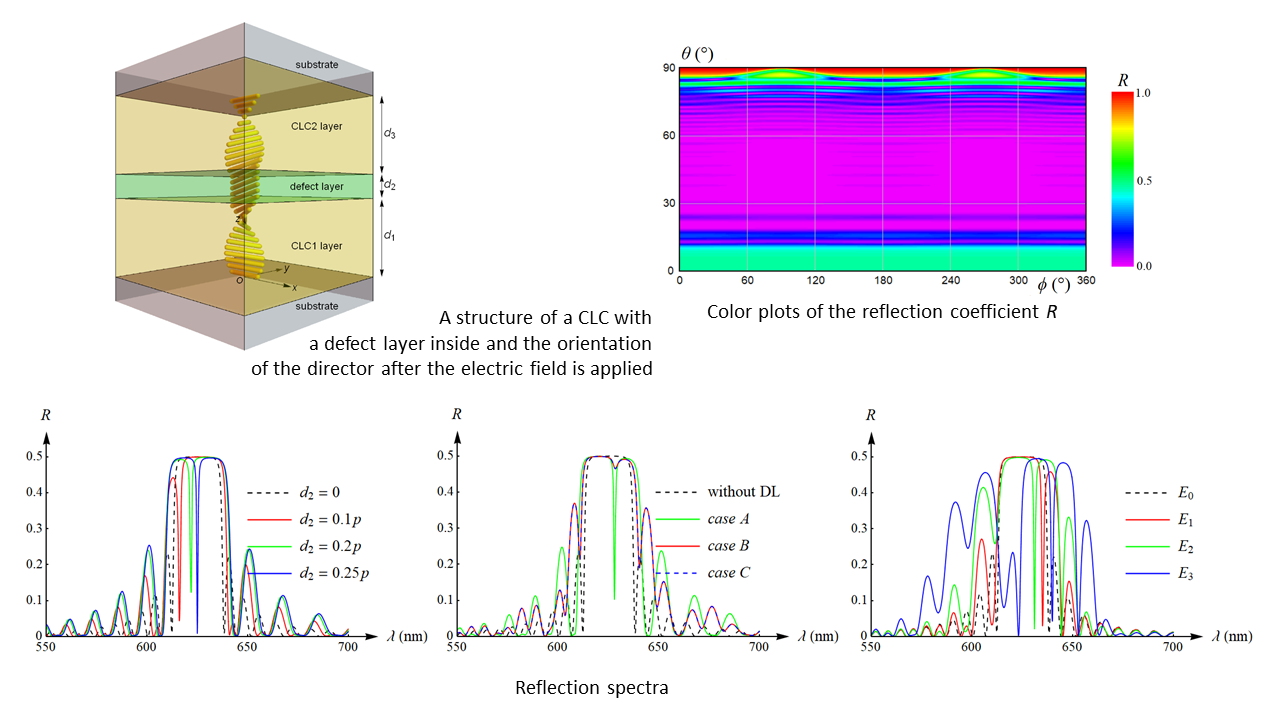
Figure 1.
A structure of the modeled cholesteric liquid crystal with a defect layer inside that is sandwiched between isotropic substrates, with the orientation of the director: (a) before the electric field is applied; (b) after the electric field is applied. The anisotropic defect layer is manifested by a locally constant director field in the range of the coordinate z from z = d1 to z = d1 + d2.

Figure 2.
Reflection spectra for different values of the thickness d2 of the defect layer (model 1): (a) d2 equal to 0.1 p, 0.2 p and 0.25 p; (b) d2 equal to 0.3 p, 0.4 p and 0.5 p; (c) d2 equal to 0.6 p, 0.7 p and 0.75 p; (d) d2 equal to 0.8 p, 0.9 p and 1.0 p.
Figure 2.
Reflection spectra for different values of the thickness d2 of the defect layer (model 1): (a) d2 equal to 0.1 p, 0.2 p and 0.25 p; (b) d2 equal to 0.3 p, 0.4 p and 0.5 p; (c) d2 equal to 0.6 p, 0.7 p and 0.75 p; (d) d2 equal to 0.8 p, 0.9 p and 1.0 p.

Figure 3.
Reflection spectra for different values of the thickness d2 of the defect layer (model 1): (a) d2 equal to 0.5 p, 1.0 p, 1.5 p and 2.0 p; (b) d2 equal to 0.25 p, 0.75 p, 1.25 p and 1.75 p.
Figure 3.
Reflection spectra for different values of the thickness d2 of the defect layer (model 1): (a) d2 equal to 0.5 p, 1.0 p, 1.5 p and 2.0 p; (b) d2 equal to 0.25 p, 0.75 p, 1.25 p and 1.75 p.

Figure 4.
Reflection spectra for different values of the thickness d2 of the defect layer (model 2): (a) d2 equal to 0.1 p, 0.2 p and 0.25 p; (b) d2 equal to 0.3 p, 0.4 p and 0.5 p.
Figure 4.
Reflection spectra for different values of the thickness d2 of the defect layer (model 2): (a) d2 equal to 0.1 p, 0.2 p and 0.25 p; (b) d2 equal to 0.3 p, 0.4 p and 0.5 p.

Figure 5.
Reflection spectra for different values of the thickness d2 of the defect layer (model 2): (a) d2 equal to 1.0 p, 2.0 p and 3.0 p; (b) d2 equal to 0.25 p, 0.75 p and 1.25 p.
Figure 5.
Reflection spectra for different values of the thickness d2 of the defect layer (model 2): (a) d2 equal to 1.0 p, 2.0 p and 3.0 p; (b) d2 equal to 0.25 p, 0.75 p and 1.25 p.

Figure 6.
Reflection as a function of the thickness d2 of the defect layer obtained for different values of the wavelength λ of the incident light: (a) model 1; (b) model 2. The curves interpolated based on the chosen computed values of the reflection represented by markers.
Figure 6.
Reflection as a function of the thickness d2 of the defect layer obtained for different values of the wavelength λ of the incident light: (a) model 1; (b) model 2. The curves interpolated based on the chosen computed values of the reflection represented by markers.

Figure 7.
Color plots of the reflection coefficient R (model 1) obtained for different values of the thickness d2 of the defect layer: (a) d2 = 0; (b) d2 = 0.5 p; (c) d2 = 0.75 p; (d) d2 = 3 p.
Figure 7.
Color plots of the reflection coefficient R (model 1) obtained for different values of the thickness d2 of the defect layer: (a) d2 = 0; (b) d2 = 0.5 p; (c) d2 = 0.75 p; (d) d2 = 3 p.

Figure 8.
Color plots of the reflection coefficient R (model 2) obtained for different values of the thickness d2 of the defect layer: (a) d2 = 0; (b) d2 = 0.5 p; (c) d2 = 0.75 p; (d) d2 = 3 p.
Figure 8.
Color plots of the reflection coefficient R (model 2) obtained for different values of the thickness d2 of the defect layer: (a) d2 = 0; (b) d2 = 0.5 p; (c) d2 = 0.75 p; (d) d2 = 3 p.

Figure 9.
Reflection spectra (model 2) for different locations of the defect layer and different values of the thickness d2: (a) d2 = 0.1 p; (b) d2 = 0.25 p; (c) d2 = 0.5 p; (d) d2 = 0.8 p.
Figure 9.
Reflection spectra (model 2) for different locations of the defect layer and different values of the thickness d2: (a) d2 = 0.1 p; (b) d2 = 0.25 p; (c) d2 = 0.5 p; (d) d2 = 0.8 p.

Figure 10.
Color plots of the reflection coefficient (model 2) obtained for d2 = 0.1 p and different locations of the defect layer: (a) case A; (b) case B; (c) case C. (d) Reflection as a function of the angle θ computed for ϕ = 0 and different locations of the defect layer.
Figure 10.
Color plots of the reflection coefficient (model 2) obtained for d2 = 0.1 p and different locations of the defect layer: (a) case A; (b) case B; (c) case C. (d) Reflection as a function of the angle θ computed for ϕ = 0 and different locations of the defect layer.

Figure 11.
Director field deformations obtained for different values of the amplitudes of the applied electric field: (a) the tilt angle θc; (b) the relative deformation of the angle ϕc–ϕc0 in relation to the angle ϕc0 obtained for the case of the undeformed director field.
Figure 11.
Director field deformations obtained for different values of the amplitudes of the applied electric field: (a) the tilt angle θc; (b) the relative deformation of the angle ϕc–ϕc0 in relation to the angle ϕc0 obtained for the case of the undeformed director field.

Figure 12.
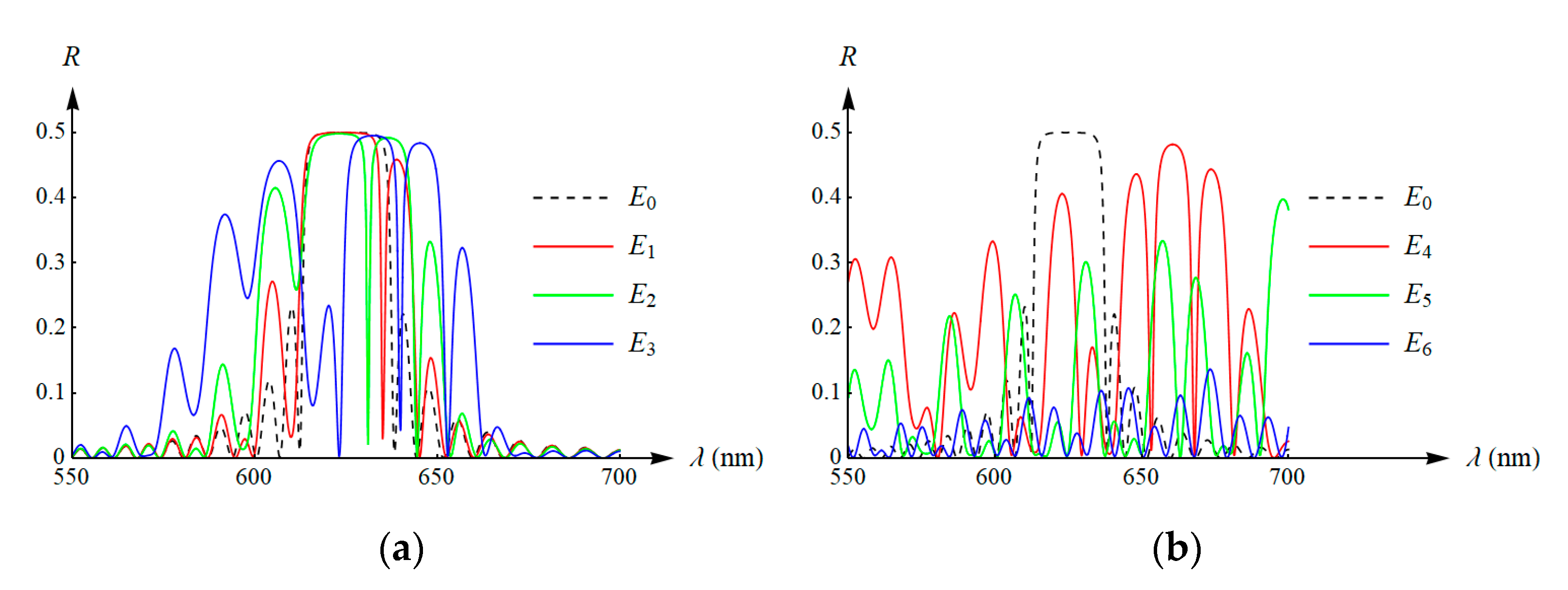
Reflection spectra of model 2 without the defect layer (d2 = 0) calculated for different values of the amplitude of the external applied electric field: (a) low electric field with the amplitudes E1, E2, and E3; (b) high electric field with the amplitudes E4, E5, and E6.
Figure 12.
Reflection spectra of model 2 without the defect layer (d2 = 0) calculated for different values of the amplitude of the external applied electric field: (a) low electric field with the amplitudes E1, E2, and E3; (b) high electric field with the amplitudes E4, E5, and E6.

Figure 13.
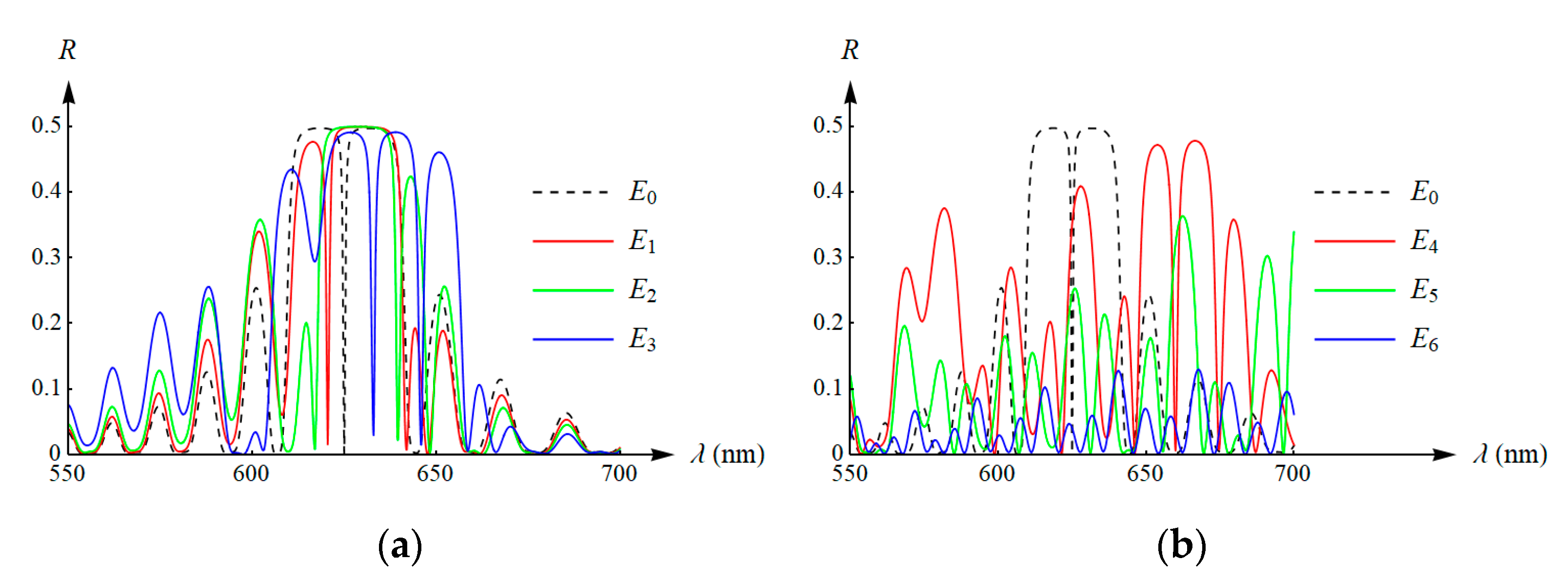
Reflection spectra of model 2 with a defect layer d2 = 0.25 p calculated for different values of the amplitude of the external applied electric field: (a) low electric field with the amplitudes E1, E2, and E3; (b) high electric field with the amplitudes E4, E5, and E6.
Figure 13.
Reflection spectra of model 2 with a defect layer d2 = 0.25 p calculated for different values of the amplitude of the external applied electric field: (a) low electric field with the amplitudes E1, E2, and E3; (b) high electric field with the amplitudes E4, E5, and E6.

Figure 14.
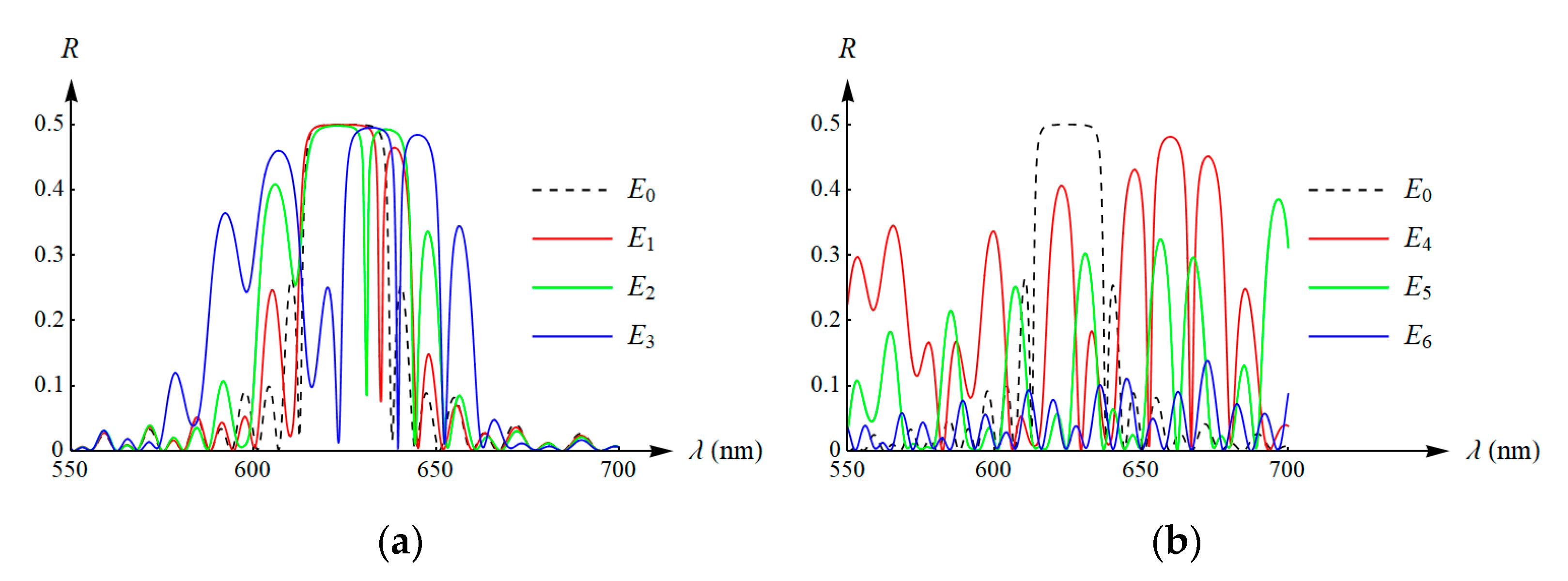
Reflection spectra of model 2 with a defect layer d2 = 0.5 p calculated for different values of the amplitude of the external applied electric field: (a) low electric field with the amplitudes E1, E2, and E3; (b) high electric field with the amplitudes E4, E5, and E6.
Figure 14.
Reflection spectra of model 2 with a defect layer d2 = 0.5 p calculated for different values of the amplitude of the external applied electric field: (a) low electric field with the amplitudes E1, E2, and E3; (b) high electric field with the amplitudes E4, E5, and E6.

Figure 15.
Reflection spectra of model 2 for different thickness of the defect layer and different values of the amplitude of the external applied electric field: (a) E = E0; (b) E = E1; (c) E = E2; (d) E = E3.
Figure 15.
Reflection spectra of model 2 for different thickness of the defect layer and different values of the amplitude of the external applied electric field: (a) E = E0; (b) E = E1; (c) E = E2; (d) E = E3.

© 2020 by the authors. Licensee MDPI, Basel, Switzerland. This article is an open access article distributed under the terms and conditions of the Creative Commons Attribution (CC BY) license (http://creativecommons.org/licenses/by/4.0/).
Share and Cite
MDPI and ACS Style
Grzelczyk, D.; Awrejcewicz, J. Reflectivity of Cholesteric Liquid Crystals with an Anisotropic Defect Layer Inside. Photonics 2020, 7, 58. https://doi.org/10.3390/photonics7030058
AMA Style
Grzelczyk D, Awrejcewicz J. Reflectivity of Cholesteric Liquid Crystals with an Anisotropic Defect Layer Inside. Photonics. 2020; 7(3):58. https://doi.org/10.3390/photonics7030058
Chicago/Turabian StyleGrzelczyk, Dariusz, and Jan Awrejcewicz. 2020. "Reflectivity of Cholesteric Liquid Crystals with an Anisotropic Defect Layer Inside" Photonics 7, no. 3: 58. https://doi.org/10.3390/photonics7030058
Note that from the first issue of 2016, this journal uses article numbers instead of page numbers. See further details here.