An Opto-Electro-Thermal Model for Black-Silicon Assisted Photovoltaic Cells in Thermophotovoltaic Applications


Abstract
:1. Introduction
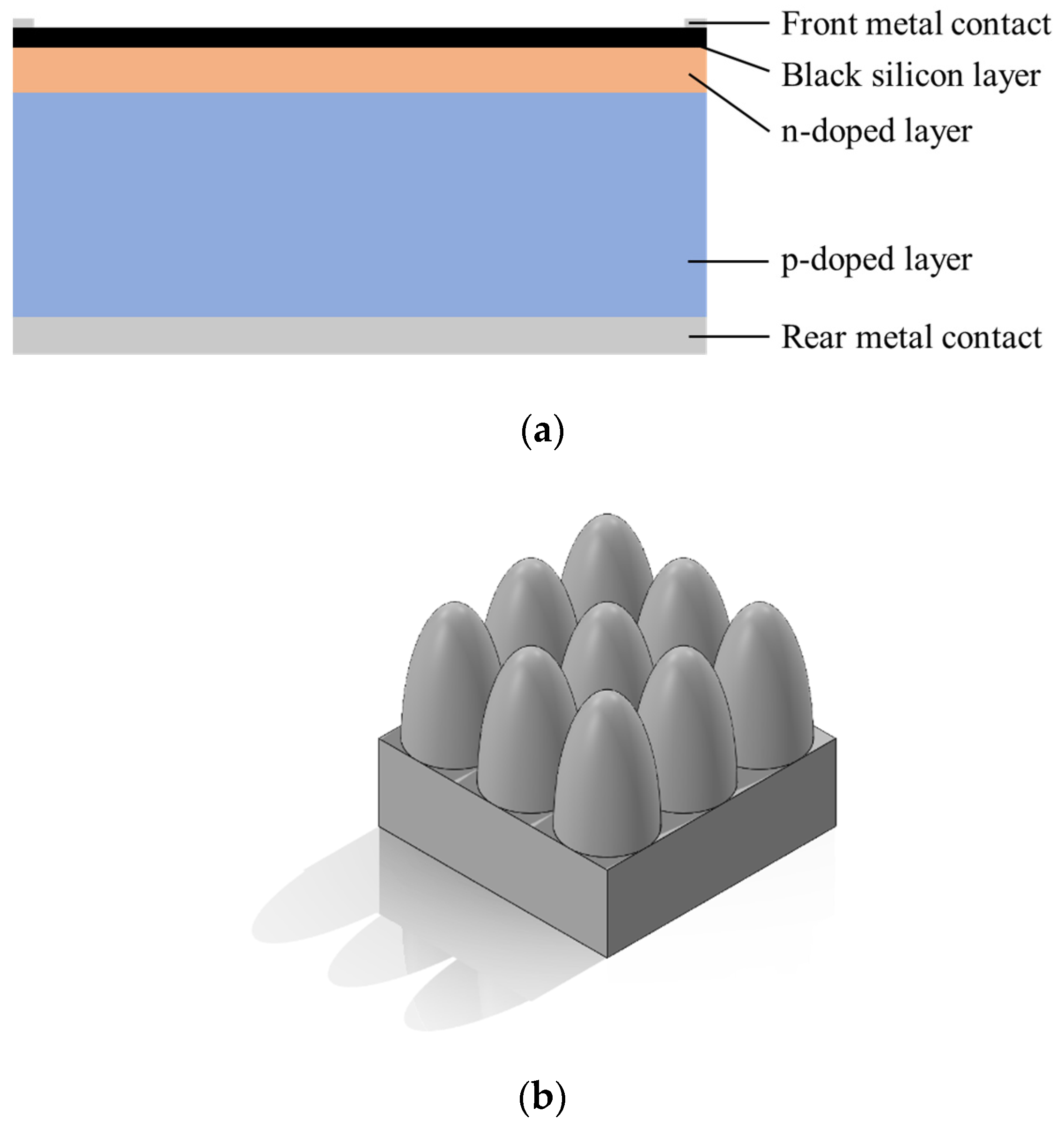
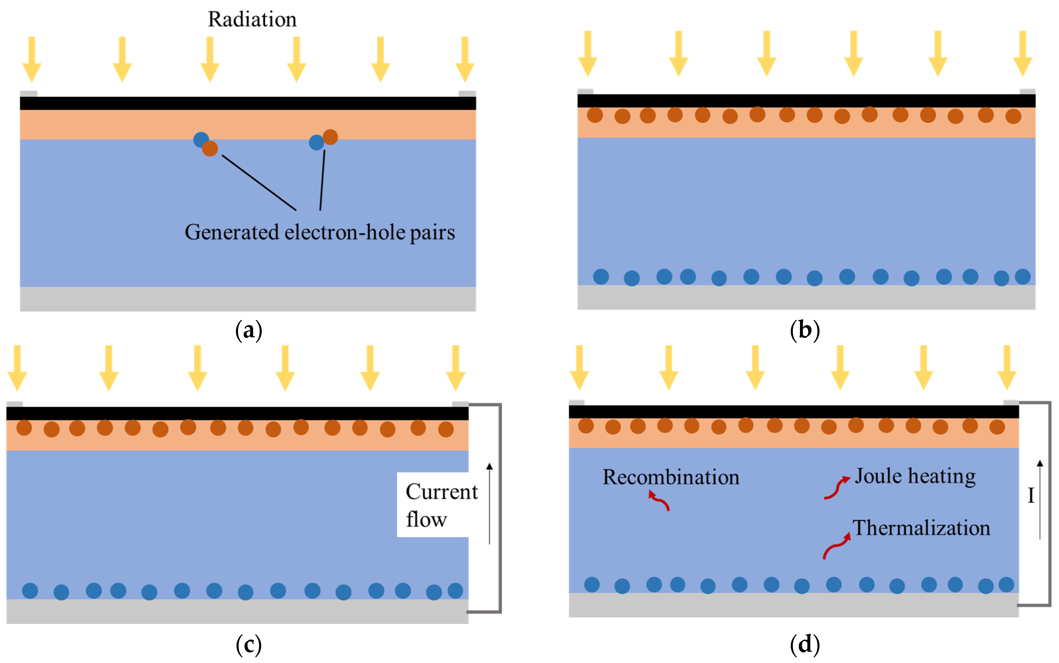
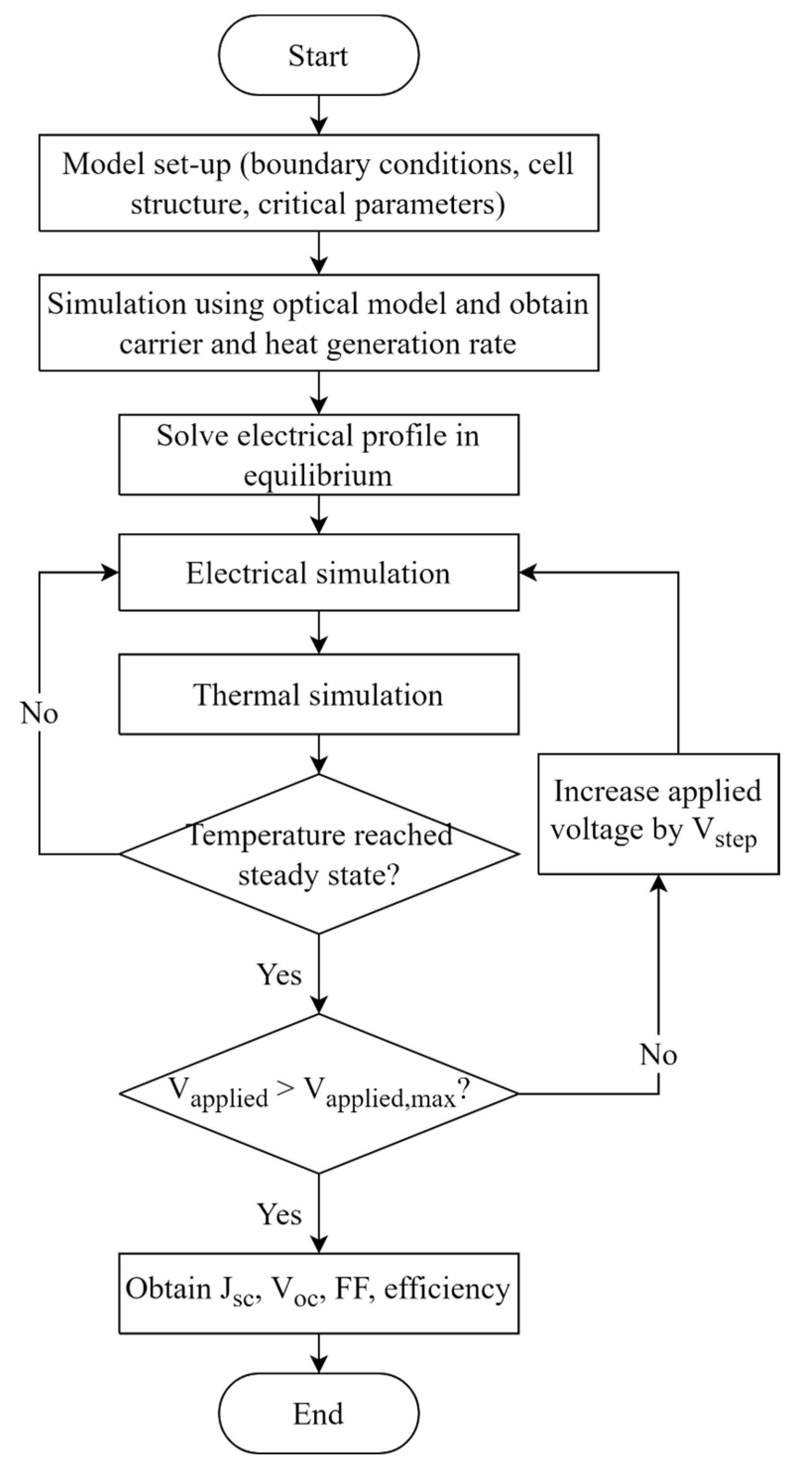
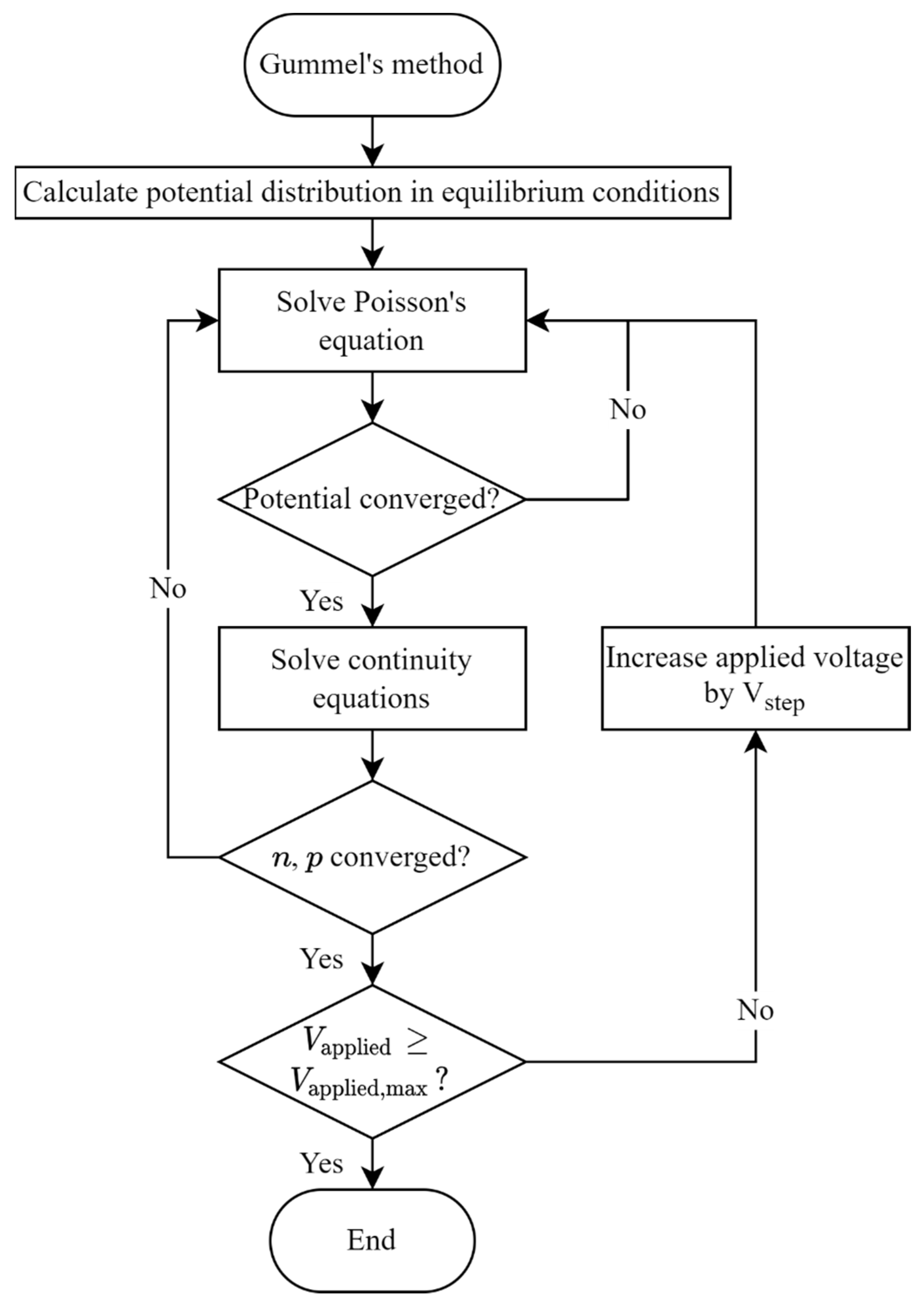
2. Methodology
2.1. Optical Model
2.2. Electrical Model
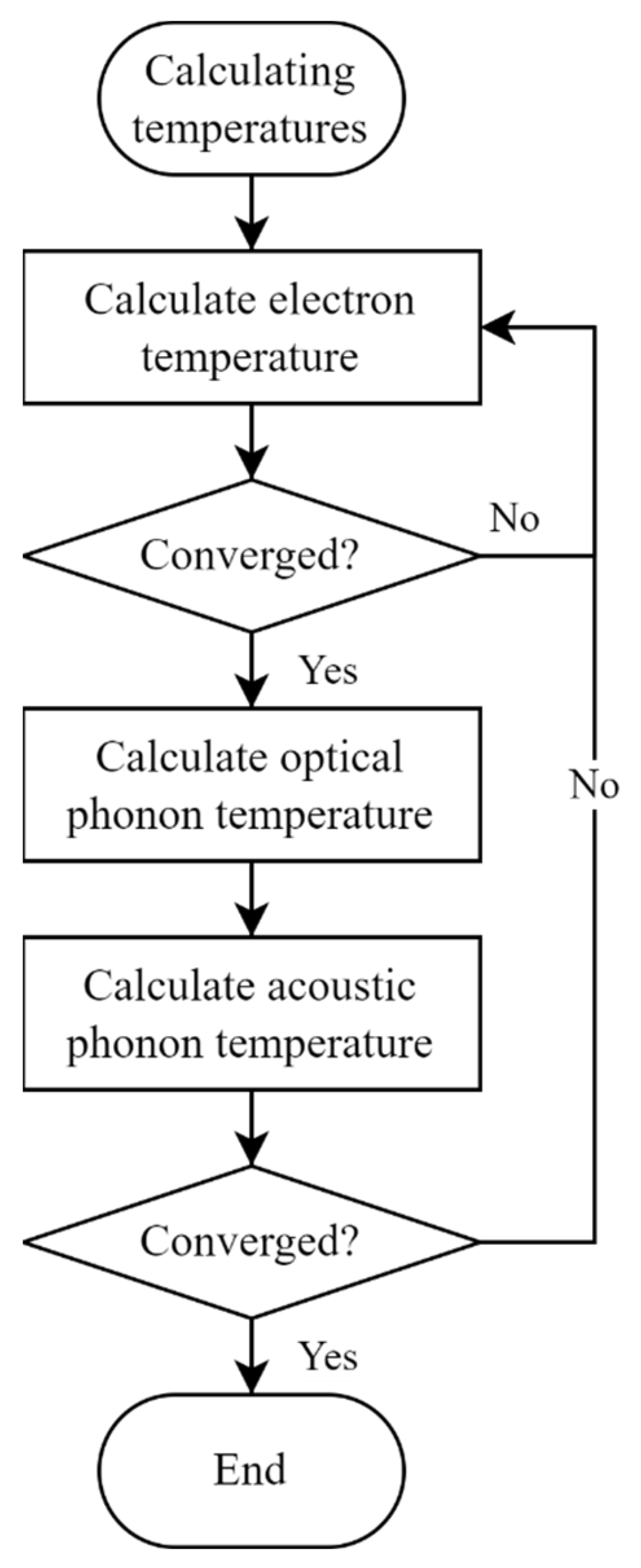
2.3. Thermal Model
3. Results
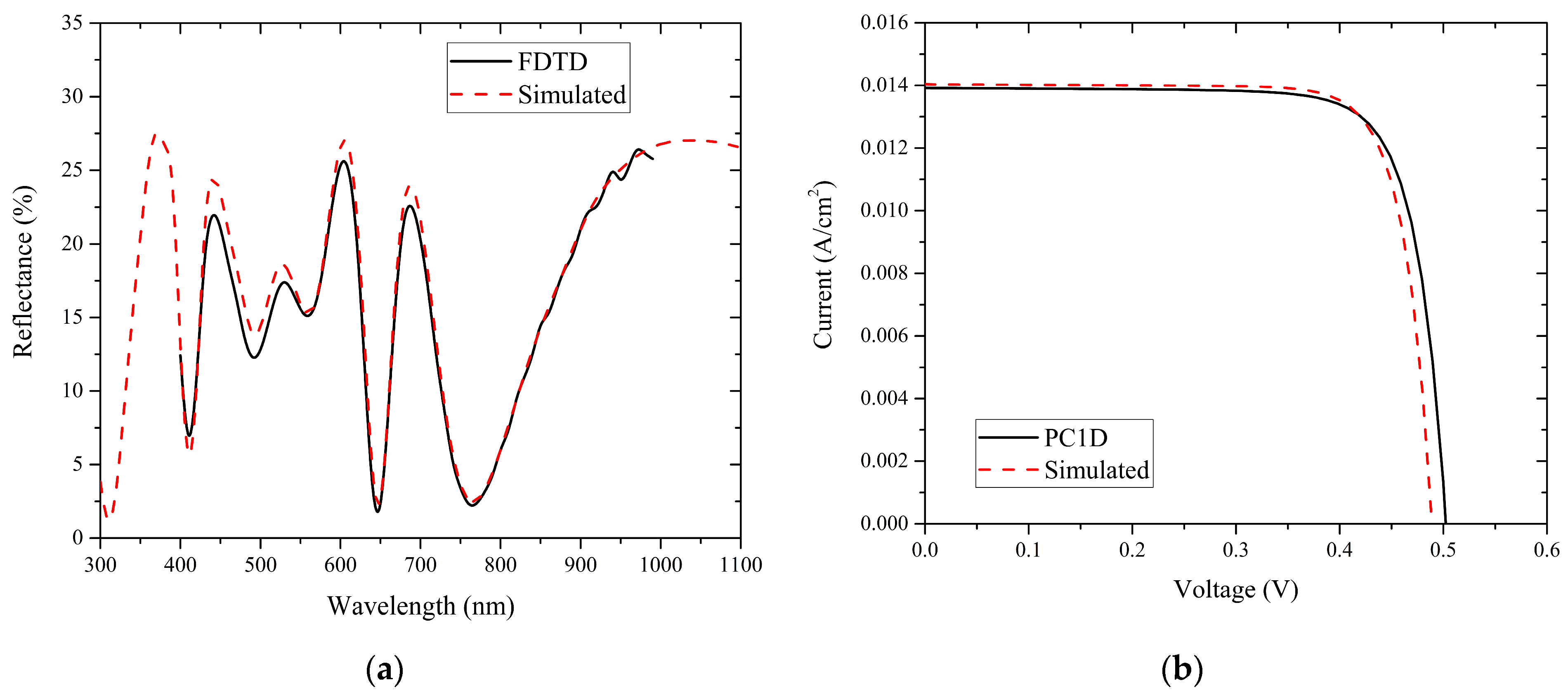
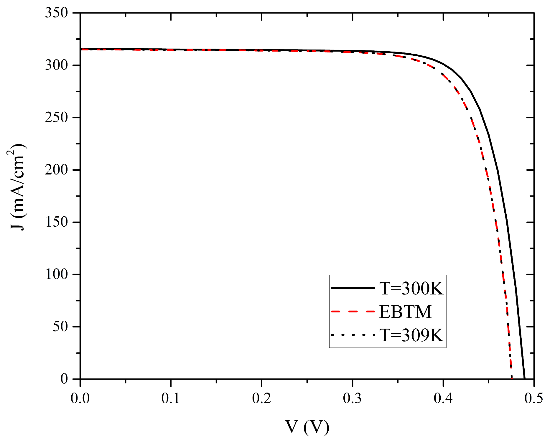
3.1. Verification of the Simulation Program
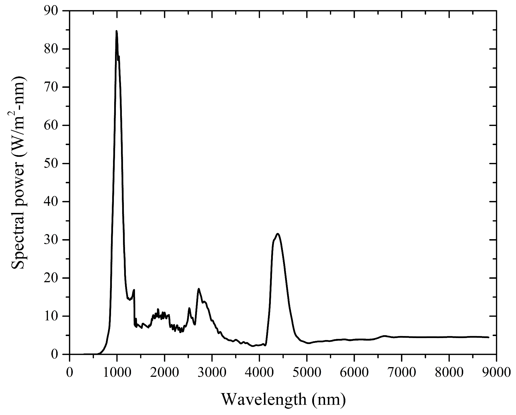
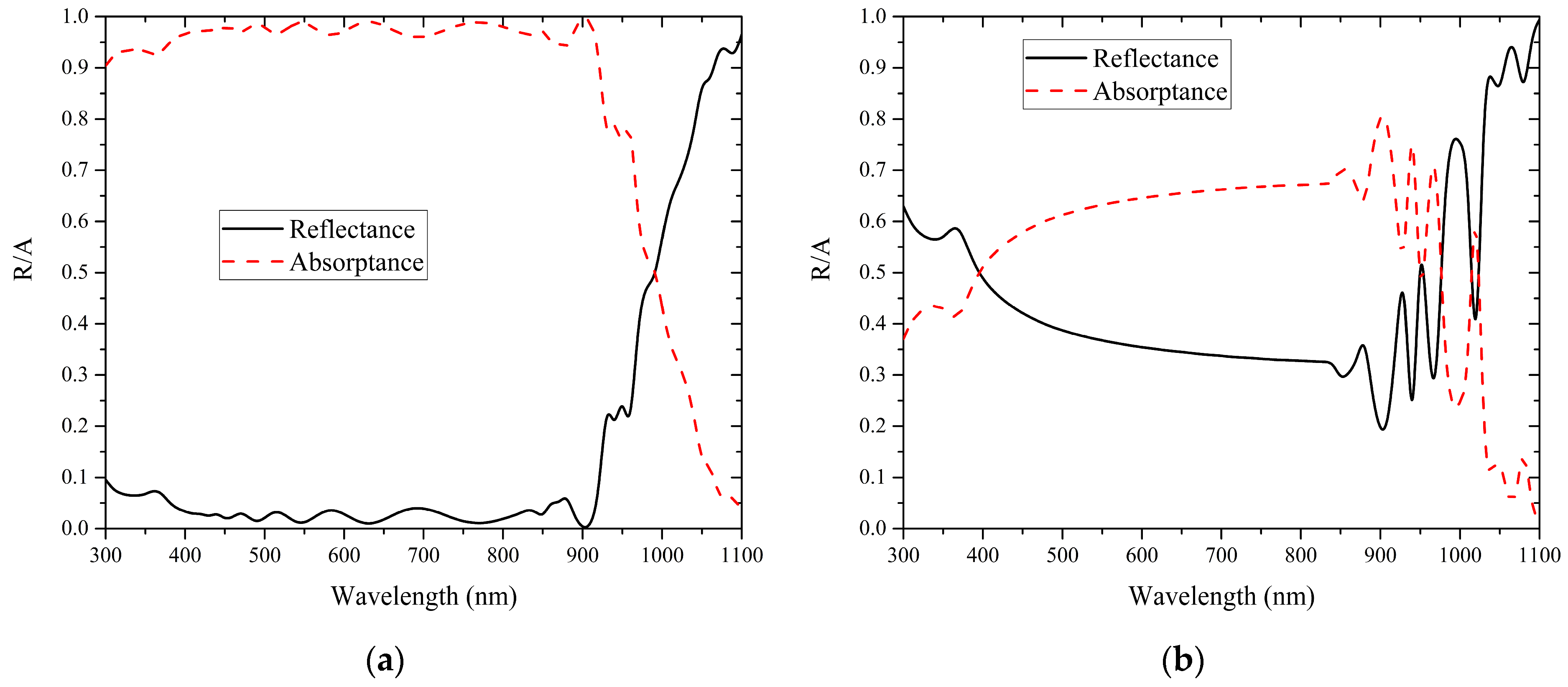
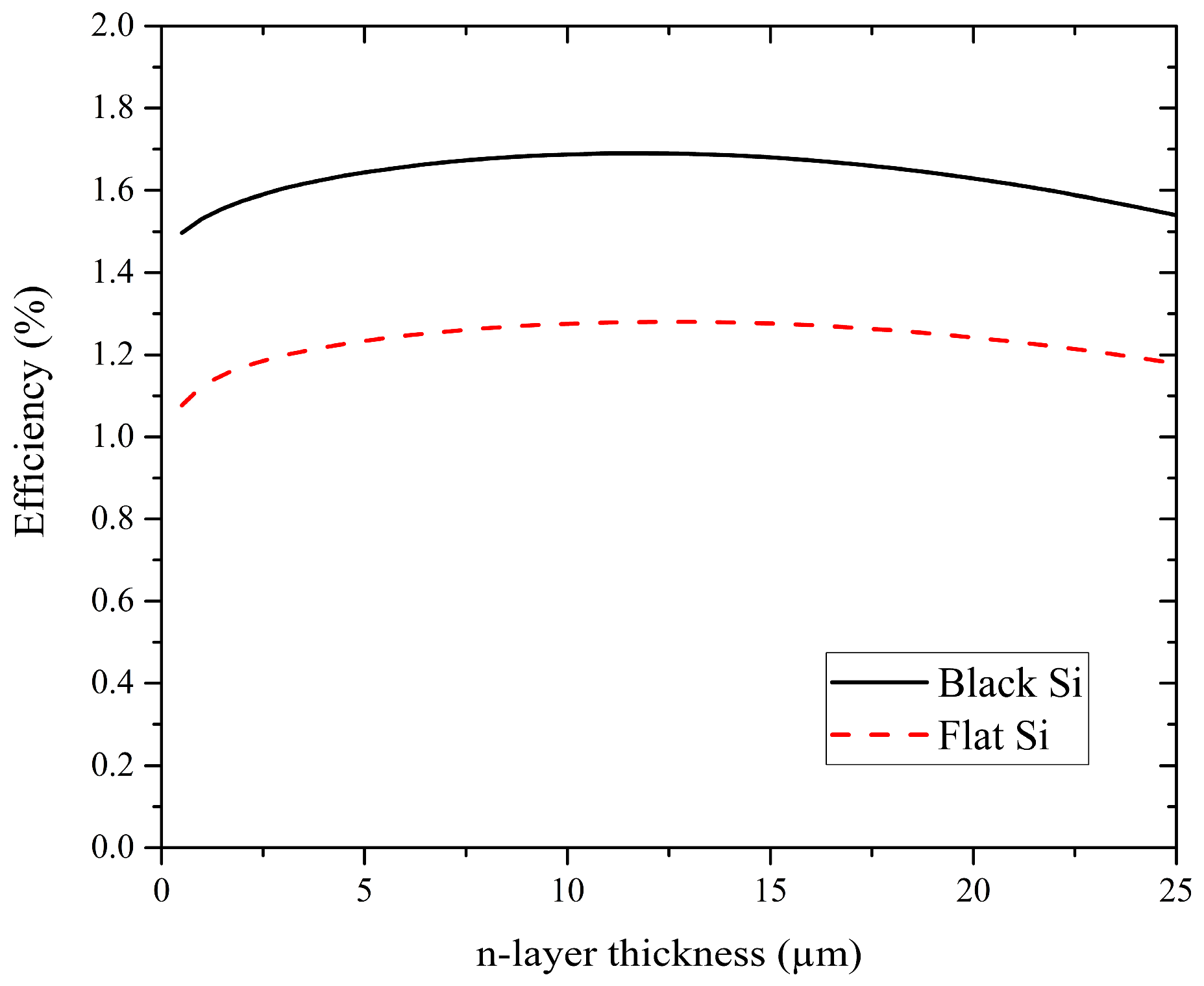
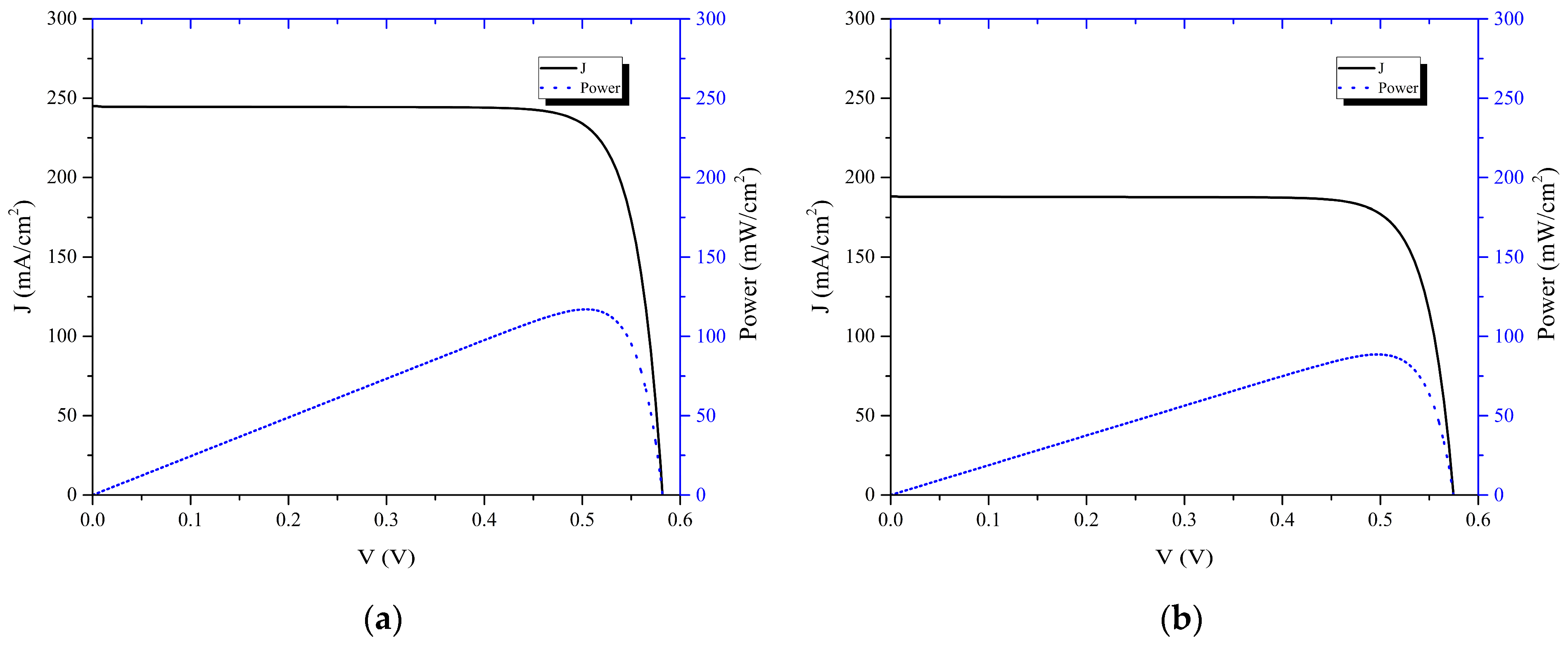
3.2. Impact of the b-Si Layer on the Thermophotovoltaic Performance
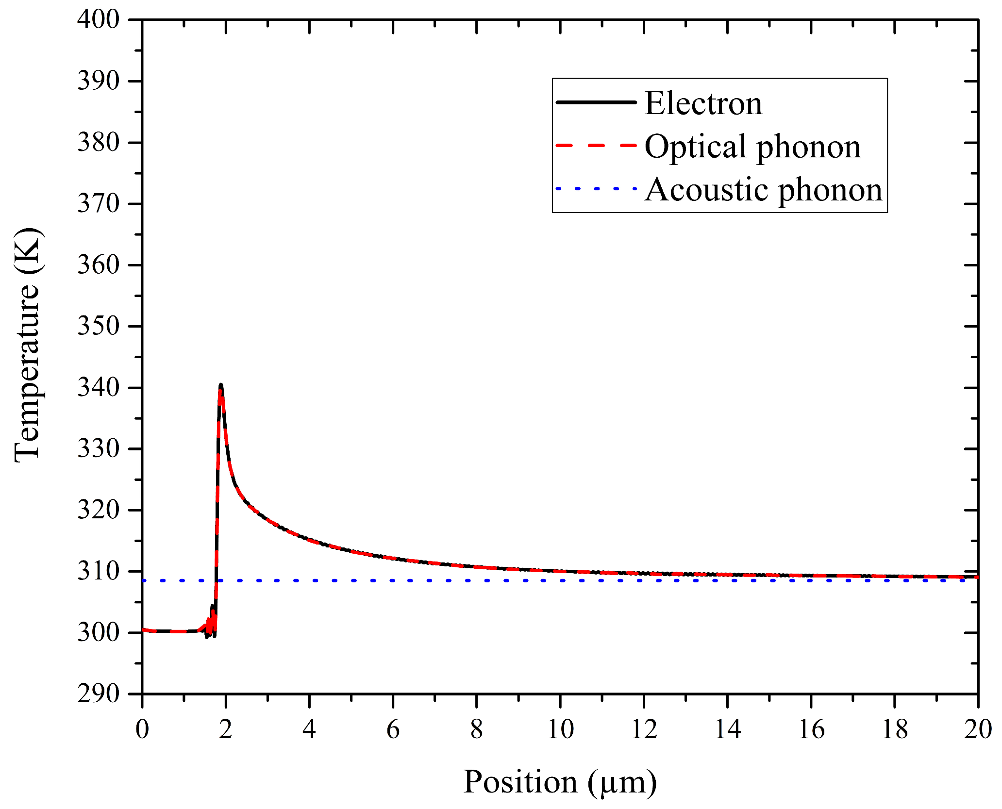
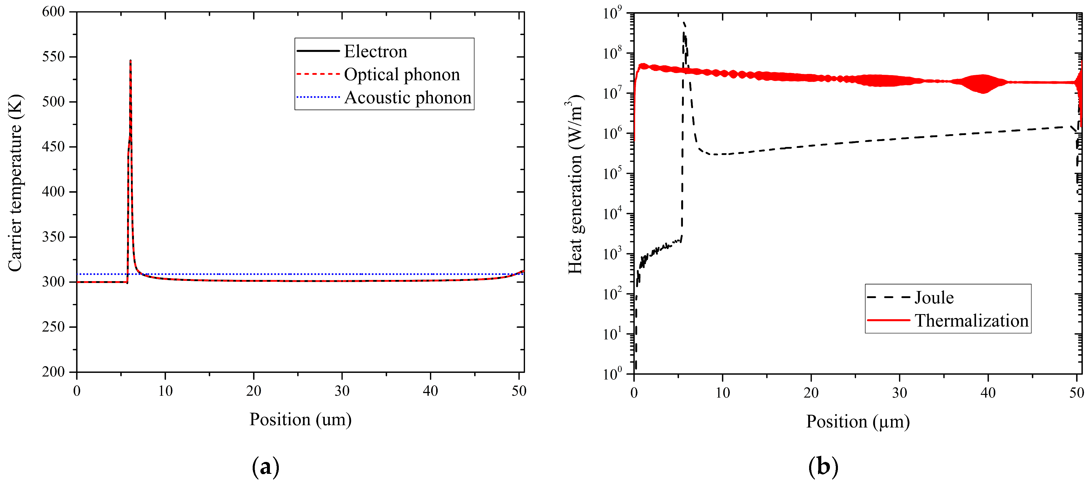
3.3. Impact of Heat Generation on Electrical Performance
4. Conclusions
Author Contributions
Funding
Institutional Review Board Statement
Informed Consent Statement
Data Availability Statement
Acknowledgments
Conflicts of Interest
References
- Chai, J.Y.H.; Wong, B.T.; Juodkazis, S. Black-silicon-assisted photovoltaic cells for better conversion efficiencies: A review on recent research and development efforts. Mater. Today Energy 2020, 18, 100539. [Google Scholar] [CrossRef]
- Elsayed, A.A.; Sabry, Y.; Marty, F.; Bourouina, T.; Khalil, D. Optical modeling of black silicon using an effective medium/multi-layer approach. Opt. Express 2018, 26, 13443. [Google Scholar] [CrossRef] [PubMed]
- Jürgen Bett, A.; Eisenlohr, J.; Höhn, O.; Repo, P.; Savin, H.; Bläsi, B.; Goldschmidt, J.C. Wave optical simulation of the light trapping properties of black silicon surface textures. Opt. Express 2016, 24, A434–A445. [Google Scholar] [CrossRef]
- Kroll, M.; Otto, M.; Käsebier, T.; Füchsel, K.; Wehrspohn, R.; Kley, E.-B.; Tünnermann, A.; Pertsch, T. Black silicon for solar cell applications. In Photonics for Solar Energy Systems IV; SPIE: Bellingham, WA, USA, 2012; Volume 8438, pp. 248–258. [Google Scholar] [CrossRef]
- Lin, C.; Povinelli, M.L. Optical absorption enhancement in silicon nanowire arrays with a large lattice constant for photovoltaic applications. Opt. Express 2009, 17, 19371–19381. [Google Scholar] [CrossRef] [PubMed]
- Ma, S.; Liu, S.; Xu, Q.; Xu, J.; Lu, R.; Liu, Y.; Zhong, Z. A theoretical study on the optical properties of black silicon. AIP Adv. 2018, 8, 035010. [Google Scholar] [CrossRef]
- Nguyen, K.; Abi-Saab, D.; Basset, P.; Richalot, E.; Malak, M.; Pavy, N.; Flourens, F.; Marty, F.; Angelescu, D.; Leprince-Wang, Y.; et al. Study of black silicon obtained by cryogenic plasma etching: Approach to achieve the hot spot of a thermoelectric energy harvester. Microsyst. Technol. 2012, 18, 1807–1814. [Google Scholar] [CrossRef]
- Nguyen, K.N.; Abi-Saab, D.; Malak, M.; Basset, P.; Richalot, E.; Pavy, N.; Flourens, F.; Marty, F.; Angelescu, D.; Leprince-Wang, Y.; et al. Study of black silicon obtained by deep reactive ion etching—Approach to achieving the hot spot of a thermoelectric energy harvester. In Proceedings of the DTIP 2011—Symposium on Design, Test, Integration and Packaging of MEMS/MOEMS, Aix-en-Provence, France, 11–13 May 2011. [Google Scholar]
- Patchett, S.; Khorasaninejad, M.; Nixon, O.; Saini, S. Effective index approximation for ordered silicon nanowire arrays. J. Opt. Soc. Am. B 2013, 30, 306. [Google Scholar] [CrossRef]
- Rahman, T.; Boden, S.A. Optical modeling of black silicon for solar cells using effective index techniques. IEEE J. Photovolt. 2017, 7, 1556–1562. [Google Scholar] [CrossRef]
- Rahman, T.; Bonilla, R.S.; Nawabjan, A.; Wilshaw, P.R.; Boden, S.A. Passivation of all-angle black surfaces for silicon solar cells. Sol. Energy Mater Sol. Cells 2017, 160, 444–453. [Google Scholar] [CrossRef]
- Ravindra, N. Modeling of optical properties of black silicon/crystalline silicon. J. Sci. Ind. Metrol. 2015, 1, 100001. [Google Scholar] [CrossRef]
- Steglich, M.; Käsebier, T.; Zilk, M.; Pertsch, T.; Kley, E.-B.; Tünnermann, A. The structural and optical properties of black silicon by inductively coupled plasma reactive ion etching. J. Appl. Phys. 2014, 116, 173503. [Google Scholar] [CrossRef]
- Tucher, N.; Gebrewold, H.T.; Blasi, B. Field stitching approach for the wave optical modeling of black silicon structures. Opt. Express 2018, 26, A937–A945. [Google Scholar] [CrossRef] [PubMed]
- Tyson, J.; Rahman, T.; Boden, S. Optical simulation of black silicon surfaces using geometric randomisation and unit-cell based averaging. In Proceedings of the 15th Photovoltaic Science, Application and Technology Conference, Coventry, UK, 10–12 April 2019; pp. 1–4. [Google Scholar]
- Wang, B.; Leu, P.W. Enhanced absorption in silicon nanocone arrays for photovoltaics. Nanotechnology 2012, 23, 194003. [Google Scholar] [CrossRef] [PubMed]
- Chai, J.Y.H.; Wong, B.T.; Juodkazis, S. Comparison between one-dimensional and three-dimensional optical modelling of ordered black silicon nanostructures using effective medium approach. In Proceedings of the 10th International Conference on Nano and Materials Science 2022, Singapore, 12–14 February 2022. [Google Scholar]
- Kane, Y. Numerical solution of initial boundary value problems involving maxwell’s equations in isotropic media. IEEE Trans. Antennas Propag. 1966, 14, 302–307. [Google Scholar] [CrossRef]
- Sullivan, D.M. Electromagnetic Simulation Using the Fdtd Method, 2nd ed.; John Wiley & Sons: Hoboken, NJ, USA, 2013. [Google Scholar] [CrossRef]
- Rumpf, R. Electromagnetic Analysis Using Finite-Difference Time-Domain. Available online: https://empossible.net/academics/emp5304/ (accessed on 10 March 2022).
- Green, M.A.; Keevers, M.J. Optical properties of intrinsic silicon at 300 k. Prog. Photovolt. Res. Appl. 1995, 3, 189–192. [Google Scholar] [CrossRef]
- Wuerfel, P. Physics of Solar Cells: From Principles to New Concepts; John Wiley & Sons: Hoboken, NJ, USA, 2005. [Google Scholar] [CrossRef]
- Entner, R. Modeling and Simulation of Negative Bias Temperature Instability; AV Akademikerverlag: Judendorf-Straßengel, Austria, 2012. [Google Scholar]
- Vasileska, D.; Goodnick, S.M.; Klimeck, G. Computational Electronics: Semiclassical and Quantum Device Modeling and Simulation, 1st ed.; CRC Press: Boca Raton, FL, USA, 2010; p. 782. [Google Scholar]
- Stratton, R. Diffusion of hot and cold electrons in semiconductor barriers. Phys. Rev. 1962, 126, 2002–2014. [Google Scholar] [CrossRef]
- Grasser, T.; Ting-Wei, T.; Kosina, H.; Selberherr, S. A review of hydrodynamic and energy-transport models for semiconductor device simulation. Proc. IEEE 2003, 91, 251–274. [Google Scholar] [CrossRef]
- Atlas User’s Manual; Silvaco Inc.: Santa Clara, CA, USA, 2016.
- Vasileska, D. Introduction to dd Modeling with Padre. Available online: https://nanohub.org/resources/1516 (accessed on 16 December 2022).
- Zhou, J.; Yi, Q.; Wang, Y.; Ye, Z. Temperature distribution of photovoltaic module based on finite element simulation. Sol. Energy 2015, 111, 97–103. [Google Scholar] [CrossRef]
- Bitnar, B.; Durisch, W.; Holzner, R. Thermophotovoltaics on the move to applications. Appl. Energy 2013, 105, 430–438. [Google Scholar] [CrossRef]
- Bitnar, B.; Durisch, W.; Mayor, J.C.; Sigg, H.; Tschudi, H.R. Characterisation of rare earth selective emitters for thermophotovoltaic applications. Sol. Energy Mater Sol. Cells 2002, 73, 221–234. [Google Scholar] [CrossRef]
- Striemer, C.C.; Fauchet, P.M. Dynamic etching of silicon for broadband antireflection applications. Appl. Phys. Lett. 2002, 81, 2980–2982. [Google Scholar] [CrossRef]


| Cell thickness | 20 µm |
| N-doped layer thickness | 0.5 µm |
| Donor concentration | 1018 cm−3 |
| P-doped layer thickness | 19.5 µm |
| Acceptor concentration | 1016 cm−3 |
| Cell temperature | 300 K |
| Reference | This study | Zhou et al. [29] |
| Top glass cover thickness (µm) | N/A | 3200 |
| Encapsulant thickness (µm) | N/A | 500 |
| Silicon cell thickness (µm) | 20 | 200 |
| Backsheet layer thickness (µm) | N/A | 300 |
| Ambient temperature (K) | 300 | 303 |
| Convective heat transfer coefficient, h (W/m2-K) | 1 | 0.001 |
| Temperature rise, ΔT (K) | 8.5 | 19.7 |
| B-Si nanostructure shape | Paraboloid |
| B-Si nanostructure height | 600 nm |
| B-Si nanostructure diameter | 350 nm |
| Period of b-Si nanostructure | 350 nm |
| Cell thickness (excluding the b-Si layer) | 50 µm |
| Emitter dopant concentration | 1017 cm−3 |
| Base dopant concentration | 1017 cm−3 |
| Rear metal layer thickness | 300 nm |
Disclaimer/Publisher’s Note: The statements, opinions and data contained in all publications are solely those of the individual author(s) and contributor(s) and not of MDPI and/or the editor(s). MDPI and/or the editor(s) disclaim responsibility for any injury to people or property resulting from any ideas, methods, instructions or products referred to in the content. |
© 2023 by the authors. Licensee MDPI, Basel, Switzerland. This article is an open access article distributed under the terms and conditions of the Creative Commons Attribution (CC BY) license (https://creativecommons.org/licenses/by/4.0/).
Share and Cite
Chai, J.Y.-H.; Wong, B.T.; Sunarso, J. An Opto-Electro-Thermal Model for Black-Silicon Assisted Photovoltaic Cells in Thermophotovoltaic Applications. Photonics 2023, 10, 565. https://doi.org/10.3390/photonics10050565
Chai JY-H, Wong BT, Sunarso J. An Opto-Electro-Thermal Model for Black-Silicon Assisted Photovoltaic Cells in Thermophotovoltaic Applications. Photonics. 2023; 10(5):565. https://doi.org/10.3390/photonics10050565
Chicago/Turabian StyleChai, Jasman Y.-H., Basil T. Wong, and Jaka Sunarso. 2023. "An Opto-Electro-Thermal Model for Black-Silicon Assisted Photovoltaic Cells in Thermophotovoltaic Applications" Photonics 10, no. 5: 565. https://doi.org/10.3390/photonics10050565