Communication

2D Saturable Absorbers for Potential Pulse Generation in the Visible-Wavelength Band

1
Laboratory of Integrated Opto-Mechanics and Electronics, School of Optical-Electrical and Computer Engineering, University of Shanghai for Science and Technology, Shanghai 200093, China
2
School of Photoelectric Engineering, Changzhou Institute of Technology, Changzhou 213032, China
*
Authors to whom correspondence should be addressed.
These authors contributed equally to this work.
Photonics 2023, 10(5), 543; https://doi.org/10.3390/photonics10050543
Submission received: 31 March 2023 / Revised: 26 April 2023 / Accepted: 4 May 2023 / Published: 8 May 2023
(This article belongs to the Special Issue Advances in Photonic Materials and Technologies)

Abstract

:
Implementing compact, efficient, and reliable passive pulsed lasers at visible wavelengths is attractive. This paper systematically investigated the thickness-dependent optical absorption characteristics of two-dimensional materials, including graphene, transition-metal dichalcogenides, and dye films at the 532 nm wavelength band, and revealed the effects of thickness on different optical absorption parameters. The results suggested that dye films are more suitable for loss-sensitive pulsed lasers and graphene is more suitable for modulation depth-sensitive pulsed lasers, while transition-metal dichalcogenide samples have intermediate performance. It can provide guidance for the rational selection of saturable absorbers in pulsed all-fiber lasers to optimize the optical pulse performance in the visible-wavelength band.

1. Introduction

Compact and efficient visible-wavelength pulsed lasers play a significant role in the fields of micro-imaging, remote sensing, medicine, and communication due to their properties of larger photon energy, stronger penetrability, lower-gain generated active ions, etc. [1,2,3,4]. Although the proposal of high-power GaN-based blue laser diodes (LDs) solutions initiates the rapid development of visible photonics, it remains a relentless pursuit for researchers to implement a visible-wavelength laser that is as compact, easy to use, cost-effective, and reliable as an all-fiber laser. The present schemes are mainly based on optical fiber nonlinear processes with low efficiency, instability, and structural complexity [5,6,7,8]. Thus, the idea of realizing an all-fiber pulsed laser without the use of frequency conversion technology becomes attractive. The most challenging part of achieving this goal is the implementation of light sources and modulation devices [4]. For the latter, compared to active mode-locked lasers [9,10,11], passive pulsed lasers based on saturable absorbers (SAs) have advantages in terms of low complexity, low cost, and reliable performance, so further refinement of their related research is important for the development of visible-wavelength pulsed lasers.
Two-dimensional (2D) materials usually present excellent SA properties, such as large modulation depths, large nonlinear optical coefficients, and low saturation intensities [12,13,14]. Among them, graphene research is one of the hot spots due to its zero bandgap and short carrier relaxation time characteristics, and a large number of ultra-narrow pulsed fiber lasers at visible, near-infrared, and mid-infrared wavelengths have been realized [15,16,17,18]. Nevertheless, their limited absorption characteristics in the visible-wavelength band and low damage threshold limit their application in high-performance systems. Layered transition-metal dichalcogenides (TMDs) have also attracted extensive attention due to their layer-dependent bandgap properties and high nonlinear optical response [4,19,20,21,22,23,24,25,26]. Compared with bulk crystals [13], the 2D materials discussed are typically layered SA samples, whose thickness-dependent carrier dynamics, high third-order nonlinear magnetization, and broadband absorption properties have shown great potential in pulsed laser systems at visible and near-infrared wavelengths, but the presence of the bandgap limits their application at long wavelengths. In addition, they even show better absorption performance than graphene in the visible-wavelength band [27,28,29,30]. Aside from layered materials, liquid dyes, another promising organic saturable absorber, can also be used for laser pulse generation at visible wavelengths. However, their toxicity, susceptibility to bleaching, and restrictions on the laser structure hinder their further development. Although low-dimensional SA devices have shown excellent thickness-dependent capabilities in current research at infrared wavelengths [31,32,33,34,35], further research on the SA selection mechanism at visible wavelengths is still needed to improve the output performance of visible-wavelength pulsed lasers.
This paper investigates the slow saturation absorption properties of commonly used materials and structures (i.e., layered 2D graphene and MoS2 prepared by mechanical exfoliation, CdS grown by conventional CVD method, and thin films containing 3,3′-diethyloxadicarbocyanine iodide (DODCI) dye) and explores their transmission characteristics in the 532 nm visible-wavelength band. Furthermore, the thickness-dependent unsaturated loss and modulation efficiency of different samples are compared and analyzed. It can provide a theoretical basis for the preparation and selection of SAs with different parameters and guide the optimization of the output performance of pulsed fiber lasers at visible wavelengths.

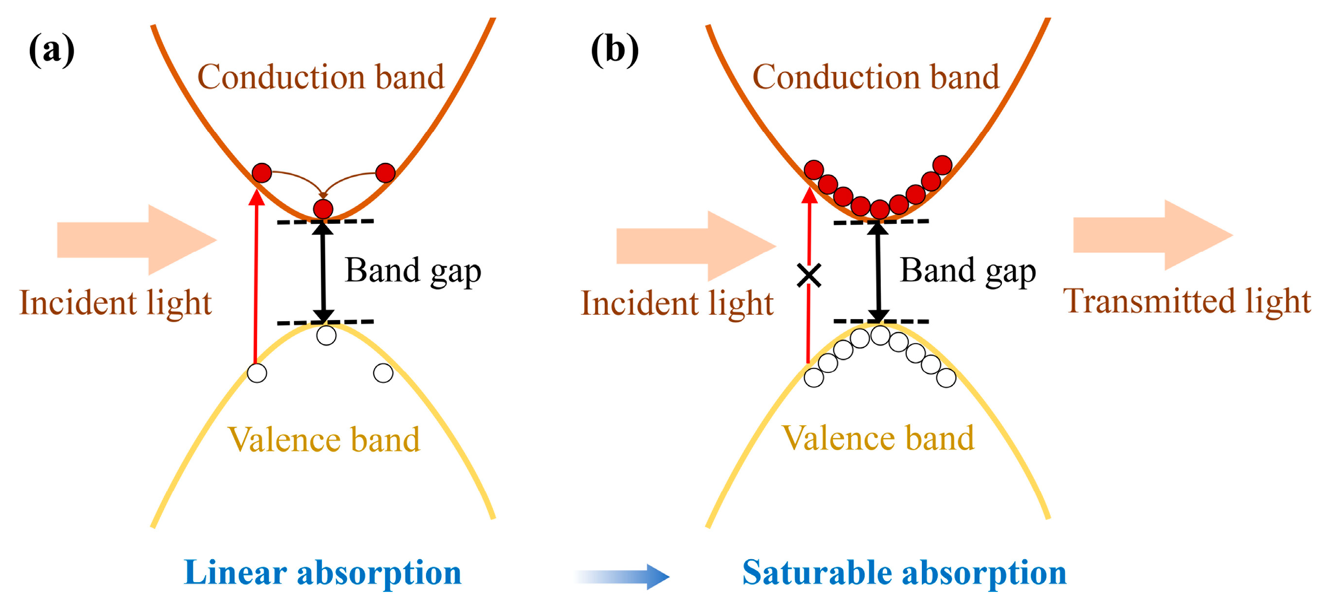
2. Theoretical Model
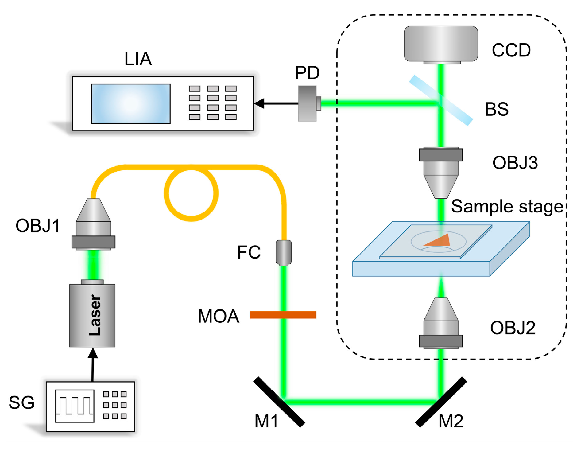
The saturable absorption effect is an intrinsic nonlinear absorption effect of the material, which is related to the third-order magnetization of the material’s electric field nonlinear response. Here the multiphoton absorption effect [36,37] is neglected, and only the saturation absorption process based on the Pauli incompatibility principle is explored. In the experiment, samples placed in the light field first show linear absorption of photons, and electrons in the internal valence band absorb photon energy and leap to the conduction band. Here, only the photon energy that satisfies the conditions for the electron leap in the valence band can be absorbed. When the external illumination time τ h is higher than the carrier recovery time τ r of the sample, with the increase in light energy, the electrons in the sample are continuously excited to the conduction band, and the photon absorption enters into a nonlinear process until the conduction band is filled. At this time, the sample macroscopically shows its absorption saturation state, and the saturation density of excited carriers can be expressed as [13,14,15]:
N s = α I s τ r h υ ,
where I s is the light intensity when the transmittance reaches half of the sample’s maximum value, α denotes the material absorption loss, τ r denotes the carrier recovery time, and h υ denotes the photon energy. According to the Pauli incompatibility principle, the electrons excited into the conduction band are sequentially arranged from low to high energy states, as shown in Figure 1, and the valence band electrons are redistributed to satisfy the Fermi-Dirac distribution. The transmission properties of the SAs in the saturable absorption process are expressed as:
T ( I ) = 1 α s 1 + I ( t ) / I s α ns ,
where I ( t ) denotes the input light intensity, α s denotes the saturation loss, and α ns denotes the unsaturated loss. Since the samples used in the experiment are 2D materials, such as thin sheets or films, the parameters of saturable absorption intensity I s , saturation loss α s , and unsaturated loss α ns are all related to their number of layers or thickness. To elucidate the thickness-dependent optical absorption of SA samples, their transmission properties can be rewritten as [13]:
T 0 = e δ N L ,
where δ represents the absorption cross-section δ gs for the ground state of the particles in the linear absorption state, while it represents the absorption cross-section δ es for the excited states of the particles in the saturated state, and L represents the thickness of the sample. Therefore, the thickness of a SA sample directly determines its optical loss and modulation depth, whether in the linear absorption or saturated absorption states.
As saturable absorbers, the absorption process of dye molecules is more complicated. According to the different electron spin states, the electronic states of dye molecules can be divided into a singlet state and a triplet state. In general, dye molecules absorb light energy, and their radiative transitions mainly occur between singlet states or triplet states; transitions between singlet and triplet states are forbidden. However, under high optical power conditions, when the excited particles at the high-energy level of the singlet state undergo spin reversal due to factors such as collisions, the transition from the singlet state to the triplet state will occur, and the longer life of the latter can accumulate a large number of particles, which can significantly contribute to an increase in absorber transmission.

3. Experiments

The measurement system for the visible-wavelength absorption properties of the target SA samples was shown in Figure 2, which was based on the laser intensity scanning method. A transparent substrate carrying the sample was placed on the microscope sample stage with a through hole in the center of the stage to ensure good light transmittance performance. The output of the quasi-continuous-wave-operated source (CNI, Changchun, China, MGL-III-532–300 mW) was modulated by a signal generator (Keysight, Colorado Springs, CO, USA, 33522A, 30 MHz) with a frequency of 30 kHz and a duty cycle of 25%. The laser signal was collected using the objective 1 (10×, NA 0.25) and then coupled through the fiber and a collimator into a motorized controlled optical attenuator (LBTEK, CEM-FPM + EM-CV1, and Thorlabs, Newton, Nj, USA, NDC-50C-4) for optical power adjustment. Afterward, the adjusted laser signal passed through the mirrors M1, M2, and the telephoto objective 2 (20×, NA 0.4) and was coupled to the microscope sample stage from the lower through hole. The light transmitted through the sample was collected by the objective 3 (Nikon, El Segundo, CA, USA, LU Plan ELWD, 100×, NA 0.8) and then divided into two ways by the beam splitter: one into the CCD camera (Nikon, DS-Ri1) for imaging, and the other into the photodetector (Thorlabs, APD410A2, gain 1.25 × 10 6 ) for photoelectric conversion. The converted signal power was measured by a lock-in amplifier (Stanford, CA, USA, SR830).
Firstly, the reflectance values of different samples and empty substrates were measured, and the input optical powers injected into different measurement samples were calibrated. Furthermore, the optical loss of an empty substrate was used as a comparison, and its transmitted optical power, P r e f , was measured. After that, the substrate carrying a saturable absorbing sample was placed in the same position, and the transmitted optical power was measured a second time to obtain the power P s i g . The absorption of the target sample was calculated to be | P r e f / P i n p u t r e f P s i g / P i n p u t s i g | , where P i n p u t r e f and P i n p u t s i g were the calibrated input optical powers of the empty substrate and the substrate carrying a SA, respectively. During the experiment, the input optical power was first adjusted to the minimum and then made to increase steadily and slowly by controlling the rotation angle of the optical attenuator MCOA. By continuously repeating the above measurements of transmitted optical power, the absorption characteristics of the sample in the whole power tuning range could be obtained until the sample reached its saturated absorption state. The microscope-based light collection system was well suited for ultra-low-power optical signal detection, and the optical power measurements were performed by an integration module in the lock-in amplifier, suppressing the light source power jitter error caused by measurement asynchrony.
Then the experiments were conducted using MoS2, CdS, graphene flakes, and DODCI film samples of different thicknesses for SA performance testing, and Figure 3a1d1 demonstrated their optical microscope images. MoS2 and graphene flakes were obtained by the mechanical exfoliation method, while CdS flakes were obtained by the conventional CVD growth method. Following that, they were transferred to the quartz substrate. Furthermore, DODCI films were prepared by first dissolving the dye in a solution of polymethyl methacrylate (PMMA) and chloroform and then spin-coating the films. The thickness and surface roughness of the samples were measured by atomic force microscopy (AFM), as shown in Figure 3a2d2, where multilayered TMD materials with thicknesses on the order of a hundred nanometers can also be considered two-dimensional or quasi-two-dimensional materials if they are strongly constrained in their thickness direction. The measurement of the thickness and surface roughness also indicated that, ignoring the partial thickness abruptness at the considered edges, the middle of the sample had good flatness for subsequent light saturation absorption measurements.

4. Results and Discussion

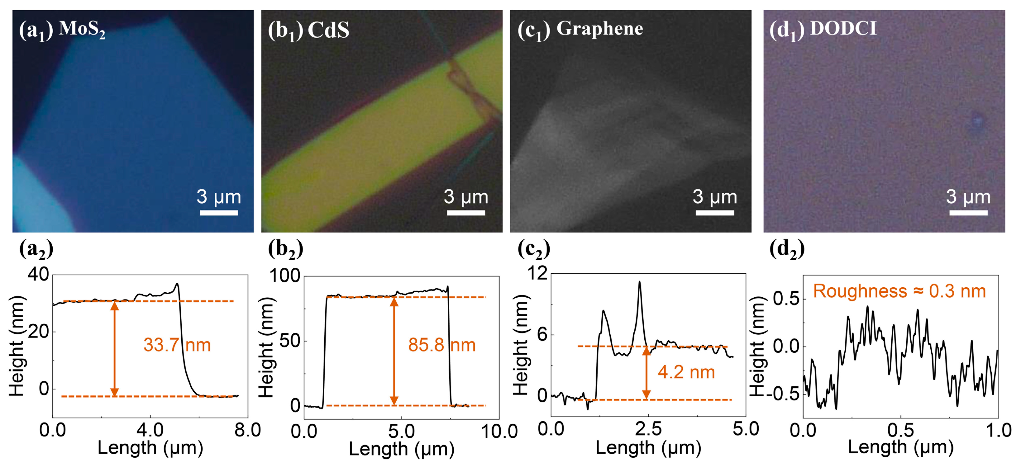
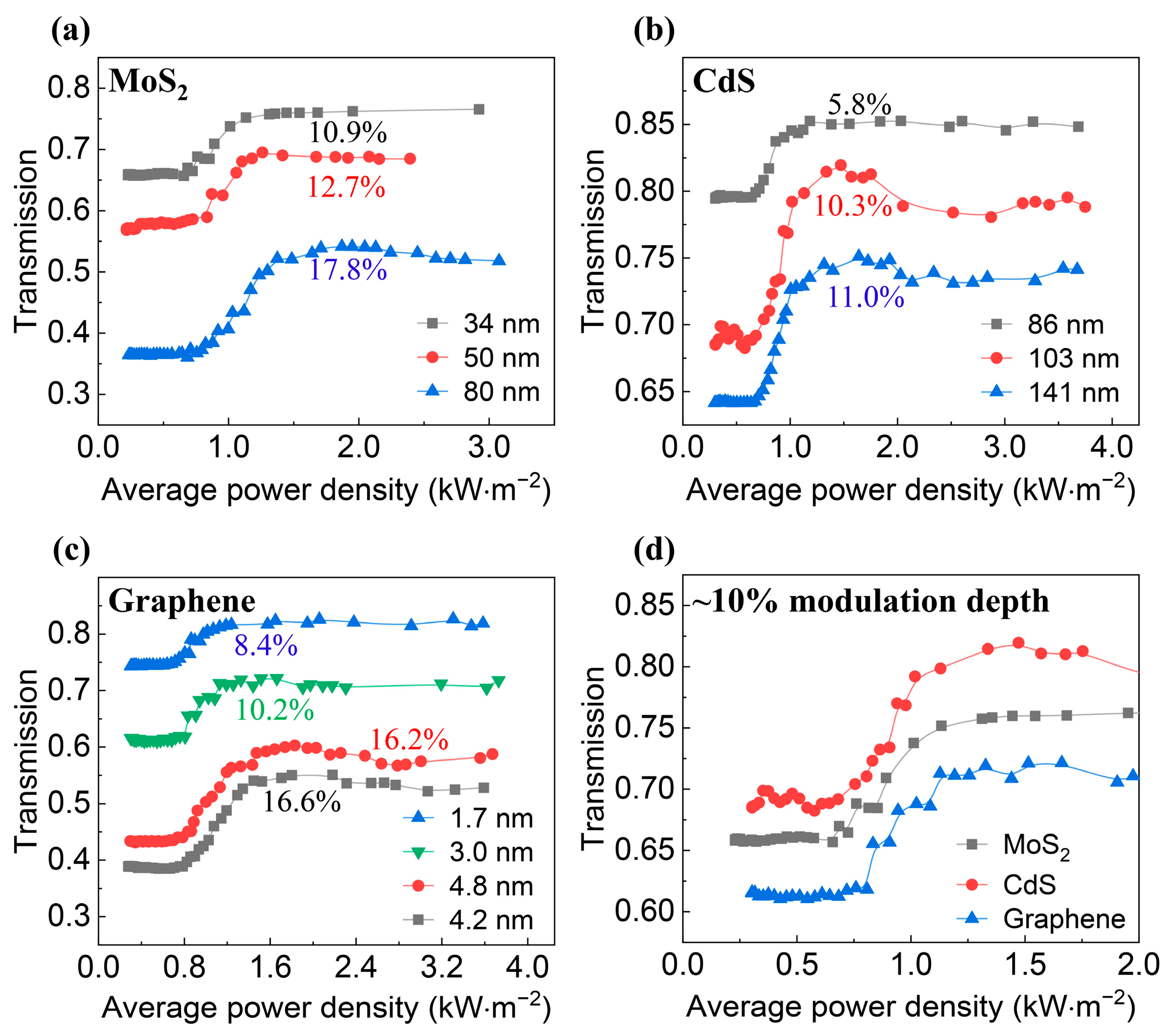
4.1. Analysis of Nonlinear Absorption Properties of Layered MoS2, CdS, and Graphene Flake

The absorption characteristics of different samples in the 532 nm visible-wavelength band were investigated separately. Figure 4 shows the light intensity-dependent nonlinear absorption properties of MoS2, CdS, and graphene flakes, which were B-spline fitted. The light intensity information was described by the light’s average power density. The precise thickness information of the sample was obtained from the AFM measurements, while the optical microscopy images were just used to select the absorption region of the samples to avoid measurement errors caused by sample thickness inhomogeneity. As shown in Figure 4a, the thickness of the selected MoS2 samples ranged from 34 to 80 nm. As the sample thickness increased, their saturation modulation depth increased from 10.9% to 17.8%, and the saturation average power density increased from 1.77 × 10 3 W·m−2 to 1.87 × 10 3 W·m−2 in the 532 nm wavelength band. Figure 4b showed the nonlinear absorption properties of CdS samples, and their thicknesses ranged from 86 to 110 nm. As the sample thickness increased, their saturation modulation depth also increased from 5.8% to 11.0%, and the saturation average power density increased from 1.38 × 10 3 W·m−2 to 1.93 × 10 3 W·m−2. As shown in Figure 4c, the thickness of the graphene samples used was less than 5 nm, their saturation modulation depth increased from 8.4% to 16.6%, and the saturation average power density increased from 1.58 × 10 3 W·m−2 to 2.18 × 10 3 W·m−2 as the thickness increased. Modulation depth and unsaturated loss of all the samples increased with the thickness of the sample. The light source used here was a quasi-continuous-wave 532 nm laser, and a pulsed laser could also be used to characterize the nonlinear absorption of the saturable absorbers. These two different measurement methods showed similar numbers of photons acting with the particles of the 2D materials in the saturated absorption state, showing that the maximum optical intensity irradiated was sufficient to produce an observable saturation absorption phenomenon.
Due to the irregular and fracture-prone characteristics of the multilayered samples prepared by the mechanical exfoliation and transfer method, gaps might exist between the substrate and the sample as well as between the layers of the sample. Thus, the thicknesses of the samples measured by AFM were higher than those calculated from the saturation modulation depth. For example, the layer number of samples in Figure 4c was 3~8, according to the linear optical absorption of ~2.3% per layer at visible wavelengths, and the measurement deviation was still within the theoretical range. In the previous work [27,28,29,30], due to different preparation methods and transfer methods, the thickness of TMD materials had a great difference, especially CdS samples, which were generally prepared as thin film forms, but the corresponding relationship between their modulation depth and unsaturated loss was approximate.
The experiments also analyzed the thickness and saturation power density parameters of different samples when the modulation depth was approximately the same, as shown in Figure 4d. To achieve the modulation depth of ~10% in the 532 nm-wavelength band, the required thicknesses of the MoS2, CdS, and graphene samples were 34 nm, 103 nm, and 3 nm, respectively. For TMDs samples, such as MoS2 and CdS, the latter required higher thicknesses, but it consistently maintained the lowest unsaturated loss and even reached 85.3% optical transmittance in the saturated state. However, the graphene sample had the lowest transmittance compared with TMD samples, although it was the thinnest.

4.2. Analysis of Nonlinear Absorption Properties of DODCI Dye Film

Thin film samples containing DODCI dye could also be used as saturable absorbers with a planar dimension close to 1 cm, and their thickness varied from a few microns at the edges to a few hundred microns at the center. In this experiment, samples were prepared with 3 mg DODCI and 150 mg PMMA. To avoid the bleaching effect of the dye, the modulation signal frequency here was reduced to 30 Hz with a duty cycle of 45%, while the output power of the 532 nm-wavelength lasers remained stable throughout the experiment. The content of dye molecules in the measurement area increased as the thickness of the film increased, leading to a consequent increase in the modulation depth of the sample, as shown in Figure 5a, where the half-edge indicated the middle of the edge and center of the film. Even at the highest modulation depth of ~24.0%, it still achieved a non-saturation loss of ~30%, which was much lower than that of 80 nm-thick MoS2 (45.9%) and 4.8 nm-thick graphene (40.0%). However, as the injection power increased, the bleaching effect of the DODCI sample made the transmittance of the sample rise slowly, and no clear saturation steady state was demonstrated, as shown by the black line in Figure 5a. DODCI dye in a liquid state could inhibit its bleaching to some extent on account of its inherent fluidity, but it would not eliminate the effect, limiting its application in high-power systems. To further explore the effect of modulated signal characteristics on the experimental results, we also investigated the saturation absorption characteristics of MoS2 samples modulated by signals with duty cycles of 45%, 65%, and 80%, respectively. Here the frequency of the modulation signal was fixed at 30 kHz, and the corresponding single-cycle illumination times of the modulated laser were 15.0, 21.7, and 26.7 μs, respectively, which were all higher than the carrier relaxation time of the sample. As shown in Figure 5b, despite the change in the single-cycle illumination times, the optical absorption characteristics of the MoS2 sample remained stable, with a saturation average power density of 3 ~ 4 × 10 3 W·m−2 and a modulation depth of ~15%.
The main measurement errors in the experiment are the thickness error of the samples and the optical power jitter error. The thickness errors of samples are caused by the non-uniform thickness of the prepared layered samples and gaps between the substrate and the sample as well as between the layers of the sample, especially for the samples prepared by mechanical exfoliation and the transfer method. The drift of the sample stage during the measurement will also cause variations in the sample thickness. The jitter error of the optical power is caused by the asynchronous measurement of the transmitted optical power of the empty substrate and the substrate carrying the sample. Although the integration circuit of the lock-in amplifier is used to suppress it, the slowly changing power shift at low frequencies will still influence the experimental results.
To select the optimal SA sample for pulse generation in visible-wavelength lasers, it is necessary to analyze all the absorption parameters. For 2D materials, the increase in thickness introduced an increase in unsaturated loss and saturation modulation depth. It was found that graphene samples got the highest thickness-dependent modulation efficiency (saturation modulation depth/thickness), but their transmittance in the visible band was less satisfactory, despite their broad absorption spectrum. While DODCI dye films have the lowest unsaturation loss of <30% at ~24% modulation depth, followed by TMDs materials. For a slow SA model, the effect of illumination time on the absorption characteristics of the samples was not noticeable. In addition, SAs with higher modulation depth, such as graphene flake, are easier to generate laser pulses with narrow linewidth and high peak power in high-power laser systems, and the unsaturated loss as an insertion loss can be compensated by increasing the input power of the optical source to reduce the impact on the output power of the optical pulse. Although DODCI dye film has excellent optical transmission and high modulation depth, it cannot be used in high-power pulsed laser systems due to its bleaching effect. However, in the case of micron- and nanometer-scale microlaser systems, whose average power value is limited by the dielectric size, SAs with lower unsaturated loss are more likely to meet their resonant gain condition.

5. Conclusions

The properties of larger photon energy and stronger penetrability have led to an increasing interest in pulsed lasers at visible wavelengths. This paper systematically investigated the saturation absorption characteristics of 2D materials, such as graphene, MoS2, CdS, and dye films containing DODCI in the visible-wavelength band. It revealed the effects of the thickness on their key parameters, such as unsaturated loss, saturation modulation depth, and saturation average power density. From the experimental results, SAs prepared by dyes and TMDs are more applicable to loss-sensitive pulsed lasers since they have lower unsaturated loss performance at visible wavelengths, such as nanolasers with ultra-high repetition frequencies, and TMD samples can be used for higher-power optical pulse systems. While SAs prepared by graphene are more applicable to depth-sensitive pulsed lasers, followed by TMD samples. The exploration of the absorption characteristics of the different 2D saturable absorbers in the 532 nm-wavelength band will provide important guidelines for the selection and optimization of pulse modulation devices for visible-wavelength lasers, which has great potential for the research of next-generation nanophotonic devices and optoelectronic devices in the visible-wavelength band.

Author Contributions

Conceptualization, F.G. and Y.M.; methodology, F.G.; writing—original draft preparation, Y.M. and R.Z.; writing—review and editing, J.P., R.Z., Y.L., T.S., Y.M. and F.G. All authors have read and agreed to the published version of the manuscript.

Funding

This work was funded by the National Natural Science Foundation of China (No. 62075131 and No. 62122054) and the Natural Science Foundation of Shanghai (No. 21ZR1481100).

Institutional Review Board Statement

Not applicable.

Informed Consent Statement

Not applicable.

Data Availability Statement

The data presented in this study are available on request from the corresponding author. The data are not publicly available due to further study.

Conflicts of Interest

The authors declare no conflict of interest.

References

  1. Shapiro, M.J.; Chow, C.C.; Karth, P.A.; Kiernan, D.F.; Blair, M.P. Effects of green diode laser in the treatment of pediatric Coats disease. Am. J. Ophthalmol. 2011, 151, 725–731.e2. [Google Scholar] [CrossRef] [PubMed]
  2. Oubei, H.M.; Duran, J.R.; Janjua, B.; Wang, H.Y.; Tsai, C.T.; Chi, Y.C.; Ng, T.K.; Kuo, H.C.; He, J.H.; Alouini, M.S.; et al. 4.8 Gbit/s 16-QAM-OFDM transmission based on compact 450-nm laser for underwater wireless optical communication. Opt. Express 2015, 23, 23302–23309. [Google Scholar] [CrossRef] [PubMed]
  3. Zhang, Y.; Yu, H.; Zhang, R.; Zhao, G.; Zhang, H.; Chen, Y.; Mei, L.; Tonelli, M.; Wang, J. Broadband atomic-layer MoS(2) optical modulators for ultrafast pulse generations in the visible range. Opt. Lett. 2017, 42, 547–550. [Google Scholar] [CrossRef] [PubMed]
  4. Luo, Z.; Wu, D.; Xu, B.; Xu, H.; Cai, Z.; Peng, J.; Weng, J.; Xu, S.; Zhu, C.; Wang, F.; et al. Two-dimensional material-based saturable absorbers: Towards compact visible-wavelength all-fiber pulsed lasers. Nanoscale 2016, 8, 1066–1072. [Google Scholar] [CrossRef]
  5. Sharping, J.E.; Foster, M.A.; Gaeta, A.L.; Lasri, J.; Lyngnes, O.; Vogel, K. Octave-spanning, high-power microstructure-fiber-based optical parametric oscillators. Opt. Express 2007, 15, 1474–1479. [Google Scholar] [CrossRef]
  6. Travers, J.C.; Popov, S.V.; Taylor, J.R. Extended blue supercontinuum generation in cascaded holey fibers. Opt. Lett. 2005, 30, 3132–3134. [Google Scholar] [CrossRef]
  7. Russell, P. Photonic crystal fibers. Science 2003, 299, 358–362. [Google Scholar] [CrossRef]
  8. Taylor, L.R.; Feng, Y.; Calia, D.B. 50W CW visible laser source at 589 nm obtained via frequency doubling of three coherently combined narrow-band Raman fibre amplifiers. Opt. Express 2010, 18, 8540–8555. [Google Scholar] [CrossRef]
  9. Kojou, J.; Watanabe, Y.; Agrawal, P.; Kamimura, T.; Kannari, F. Wavelength tunable Q-switch laser in visible region with Pr3+-doped fluoride-glass fiber pumped by GaN diode laser. Opt. Commun. 2013, 290, 136–140. [Google Scholar] [CrossRef]
  10. Ma, Y.; Jing, X.; Gu, F. Stable and Tunable Optoelectronic Oscillator With External Stimulated Brillouin Beat Note Injection. IEEE Photonics Technol. Lett. 2021, 33, 1085–1088. [Google Scholar] [CrossRef]
  11. Zou, J.; Dong, C.; Wang, H.; Du, T.; Luo, Z. Towards visible-wavelength passively mode-locked lasers in all-fibre format. Light. Sci. Appl. 2020, 9, 61. [Google Scholar] [CrossRef] [PubMed]
  12. Liu, X.; Gao, Q.; Zheng, Y.; Mao, D.; Zhao, J. Recent progress of pulsed fiber lasers based on transition-metal dichalcogenides and black phosphorus saturable absorbers. Nanophotonics 2020, 9, 2215–2231. [Google Scholar] [CrossRef]
  13. Wang, G.; Baker-Murray, A.A.; Blau, W.J. Saturable Absorption in 2D Nanomaterials and Related Photonic Devices. Laser Photonics Rev. 2019, 13, 1800282. [Google Scholar] [CrossRef]
  14. Zhang, B.T.; Liu, J.; Wang, C.; Yang, K.J.; Lee, C.; Zhang, H.; He, J.L.O. Recent Progress in 2D Material-Based Saturable Absorbers for All Solid-State Pulsed Bulk Lasers. Laser Photonics Rev. 2020, 14, 1900240. [Google Scholar] [CrossRef]
  15. Guo, B.; Xiao, Q.L.; Wang, S.H.; Zhang, H. 2D Layered Materials: Synthesis, Nonlinear Optical Properties, and Device Applications. Laser Photonics Rev. 2019, 13, 1800327. [Google Scholar] [CrossRef]
  16. Sun, Z.; Hasan, T.; Ferrari, A.C. Ultrafast lasers mode-locked by nanotubes and graphene. Phys. E Low-Dimens. Syst. Nanostructures 2012, 44, 1082–1091. [Google Scholar] [CrossRef]
  17. Xiaohui, L.; Yulong, T.; Zhiyu, Y.; Yue, W.; Bo, M.; Guozhen, L.; Handong, S.; Xia, Y.; Ying, Z.; Xueping, C.; et al. Broadband Saturable Absorption of Graphene Oxide Thin Film and Its Application in Pulsed Fiber Lasers. IEEE J. Sel. Top. Quantum Electron. 2014, 20, 441–447. [Google Scholar] [CrossRef]
  18. Zhao, Y.; Guo, P.; Li, X.; Jin, Z. Ultrafast photonics application of graphdiyne in the optical communication region. Carbon. 2019, 149, 336–341. [Google Scholar] [CrossRef]
  19. Chen, H.; Yin, J.; Yang, J.; Zhang, X.; Liu, M.; Jiang, Z.; Wang, J.; Sun, Z.; Guo, T.; Liu, W.; et al. Transition-metal dichalcogenides heterostructure saturable absorbers for ultrafast photonics. Opt. Lett. 2017, 42, 4279–4282. [Google Scholar] [CrossRef]
  20. Bikorimana, S.; Lama, P.; Walser, A.; Dorsinville, R.; Anghel, S.; Mitioglu, A.; Micu, A.; Kulyuk, L. Nonlinear optical responses in two-dimensional transition metal dichalcogenide multilayer: WS_2, WSe_2, MoS_2 and Mo_05W_05S_2: Publisher’s note. Opt. Express 2016, 24, 26998. [Google Scholar] [CrossRef]
  21. Mao, D.; Zhang, S.; Wang, Y.; Gan, X.; Zhang, W.; Mei, T.; Wang, Y.; Wang, Y.; Zeng, H.; Zhao, J. WS_2 saturable absorber for dissipative soliton mode locking at 106 and 155 µm. Opt. Express 2015, 23, 27509–27519. [Google Scholar] [CrossRef] [PubMed]
  22. Wu, K.; Zhang, X.; Wang, J.; Chen, J. 463-MHz fundamental mode-locked fiber laser based on few-layer MoS_2 saturable absorber. Opt. Lett. 2015, 40, 1374–1377. [Google Scholar] [CrossRef] [PubMed]
  23. Zhang, M.; Hu, G.; Hu, G.; Howe, R.C.T.; Chen, L.; Zheng, Z.; Hasan, T. Yb- and Er-doped fiber laser Q-switched with an optically uniform, broadband WS2 saturable absorber. Sci. Rep. 2015, 5, 17482. [Google Scholar] [CrossRef] [PubMed]
  24. Ma, Y.; Liu, Y.; Tan, X.; Shen, T.; Gu, F. Tailoring photoluminescence and optoelectrical properties of MoS2 monolayers on Au interdigital electrodes. Jpn. J. Appl. Phys. 2022, 61, 6226–6235. [Google Scholar] [CrossRef]
  25. Yu, J.X.; Xing, S.; Dai, G.Y.; Ling-Hu, S.Y.; Gu, F.X. Direct-Bandgap Bilayer WSe(2) /Microsphere Monolithic Cavity for Low-Threshold Lasing. Adv. Mater. 2022, 34, e2106502. [Google Scholar] [CrossRef] [PubMed]
  26. Wang, K.; Wang, J.; Fan, J.; Lotya, M.; O’Neill, A.; Fox, D.; Feng, Y.; Zhang, X.; Jiang, B.; Zhao, Q.; et al. Ultrafast Saturable Absorption of Two-Dimensional MoS2 Nanosheets. ACS Nano 2013, 7, 9260–9267. [Google Scholar] [CrossRef] [PubMed]
  27. Zhang, S.; Li, Y.; Zhang, X.; Dong, N.; Wang, K.; Hanlon, D.; Coleman, J.N.; Zhang, L.; Wang, J. Slow and fast absorption saturation of black phosphorus: Experiment and modelling. Nanoscale 2016, 8, 17374–17382. [Google Scholar] [CrossRef]
  28. Shi, Z.; Gong, J.; Zhang, J.; Xu, P.; Yao, N.; Fang, W.; Wang, P.; Guo, X.; Tong, L. Single-Nanowire Thermo-Optic Modulator Based on a Varshni Shift. ACS Photonics 2020, 7, 2571–2577. [Google Scholar] [CrossRef]
  29. Yuan, X.; Wang, F.; Liang, Y.; Zhu, B.; Gu, Y. Enhanced nonlinear optical properties of reduced graphene oxide modified by Mn-doped semiconductor CdS nanoparticles as photonic materials. J. Phys. D Appl. Phys. 2022, 55, 344004. [Google Scholar] [CrossRef]
  30. Zhang, Y.; Wang, S.; Wang, D.; Yu, H.; Zhang, H.; Chen, Y.; Mei, L.; Di Lieto, A.; Tonelli, M.; Wang, J. Atomic-Layer Molybdenum Sulfide Passively Modulated Green Laser Pulses. IEEE Photonics Technol. Lett. 2016, 28, 197–200. [Google Scholar] [CrossRef]
  31. Li, D.; Jussila, H.; Karvonen, L.; Ye, G.; Lipsanen, H.; Chen, X.; Sun, Z. Polarization and Thickness Dependent Absorption Properties of Black Phosphorus: New Saturable Absorber for Ultrafast Pulse Generation. Sci. Rep. 2015, 5, 15899. [Google Scholar] [CrossRef] [PubMed]
  32. Ajmal, R.; Bibi, S.; Ahmed, R.; Sohail, M.; Asghar, H.; Umar, Z.A.; Shahzad, N.; Baig, M.A. The role of saturable absorbers thickness in the Q-switching of the erbium-doped fiber laser. Laser Phys. Lett. 2023, 20, 035101. [Google Scholar] [CrossRef]
  33. Sobon, G.; Duzynska, A.; Świniarski, M.; Judek, J.; Sotor, J.; Zdrojek, M. CNT-based saturable absorbers with scalable modulation depth for Thulium-doped fiber lasers operating at 1.9 μm. Sci. Rep. 2017, 7, 45491. [Google Scholar] [CrossRef] [PubMed]
  34. Chiu, J.-C.; Lan, Y.-F.; Chang, C.-M.; Chen, X.-Z.; Yeh, C.-Y.; Lee, C.-K.; Lin, G.-R.; Lin, J.-J.; Cheng, W.-H. Concentration effect of carbon nanotube based saturable absorber on stabilizing and shortening mode-locked pulse. Opt. Express 2010, 18, 3592–3600. [Google Scholar] [CrossRef] [PubMed]
  35. Chiu, J.-C.; Chang, C.-M.; Hsieh, B.-Z.; Lin, S.-C.; Yeh, C.-Y.; Lin, G.-R.; Lee, C.-K.; Lin, J.-J.; Cheng, W.-H. Pulse shortening mode-locked fiber laser by thickness and concentration product of carbon nanotube based saturable absorber. Opt. Express 2011, 19, 4036–4041. [Google Scholar] [CrossRef]
  36. Dong, N.; Li, Y.; Zhang, S.; McEvoy, N.; Gatensby, R.; Duesberg, G.S.; Wang, J. Saturation of Two-Photon Absorption in Layered Transition Metal Dichalcogenides: Experiment and Theory. ACS Photonics 2018, 5, 1558–1565. [Google Scholar] [CrossRef]
  37. Linghu, S.; Ma, Y.; Gu, Z.; Zhu, R.; Liu, Y.; Liu, H.; Gu, F. Thermal-mechanical-photo-activation effect on silica micro/nanofiber surfaces: Origination, reparation and utilization. Opt. Express 2022, 30, 22755–22767. [Google Scholar] [CrossRef]
Figure 1. Mechanisms of saturable absorption processes based on the Pauli incompatibility principle: (a) linear absorption process and (b) nonlinear absorption process.
Photonics 10 00543 g001
Figure 2. Detection scheme of the absorption characteristics of SA samples in the visible-wavelength band. SG: signal generator; OBJ: objective; MOA: motor-controlled optical attenuator; FC: fiber collimator; M: reflecting mirror; BS: beamsplitter; PD: photodetector; LIA: lock-in amplifier; CCD: charge-coupled device camera.
Photonics 10 00543 g002
Figure 3. (a1d1) Optical microscopic images of MoS2, CdS, graphene flakes, and DODCI thin film samples and (a2d2) their corresponding sample thickness or surface roughness information.
Photonics 10 00543 g003
Figure 4. Light intensity-dependent nonlinear absorption properties of (a) MoS2, (b) CdS, and (c) graphene flake samples, and (d) comparison of the absorption properties of different SA samples with the same ~10% modulation depth in the 532 nm-wavelength band.
Photonics 10 00543 g004
Figure 5. (a) Light intensity-dependent nonlinear absorption measurements of DODCI film samples; the inset shows the APM imaging of the DODCI films with a roughness of ~0.3 nm. (b) the effect of single-cycle illumination times on the light absorption properties of MoS2 samples.
Photonics 10 00543 g005
Disclaimer/Publisher’s Note: The statements, opinions and data contained in all publications are solely those of the individual author(s) and contributor(s) and not of MDPI and/or the editor(s). MDPI and/or the editor(s) disclaim responsibility for any injury to people or property resulting from any ideas, methods, instructions or products referred to in the content.

