An Interlayer of Ultrasmall N-Rich Carbon Dots for Optimization of SnO2/CsFAPbI3 Interface

 ,
,  , , , , , and
Abstract
:1. Introduction
2. Materials and Methods
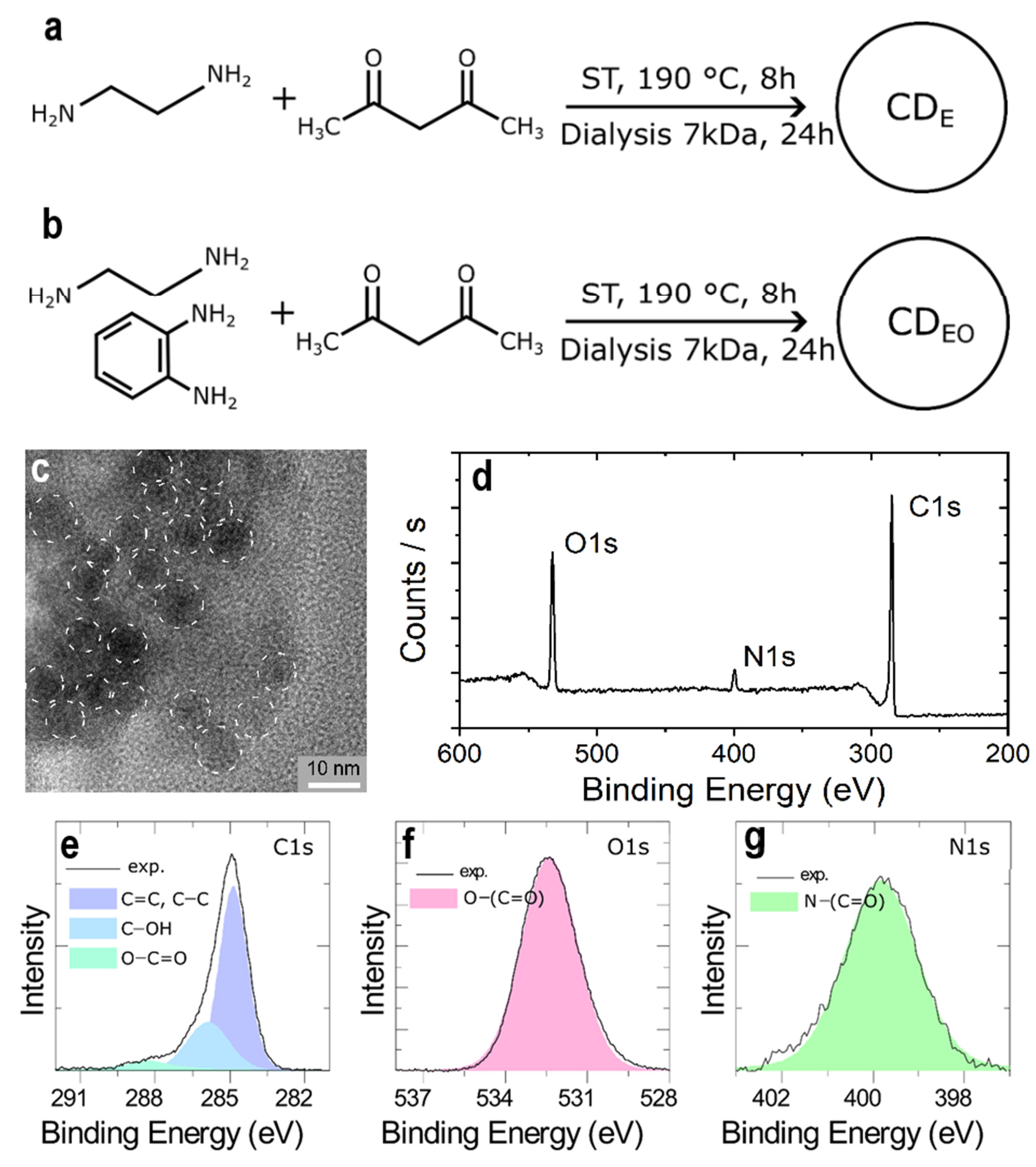
2.1. Carbon Dots (CDs) Synthesis
2.2. Thin Films and Device Fabrication
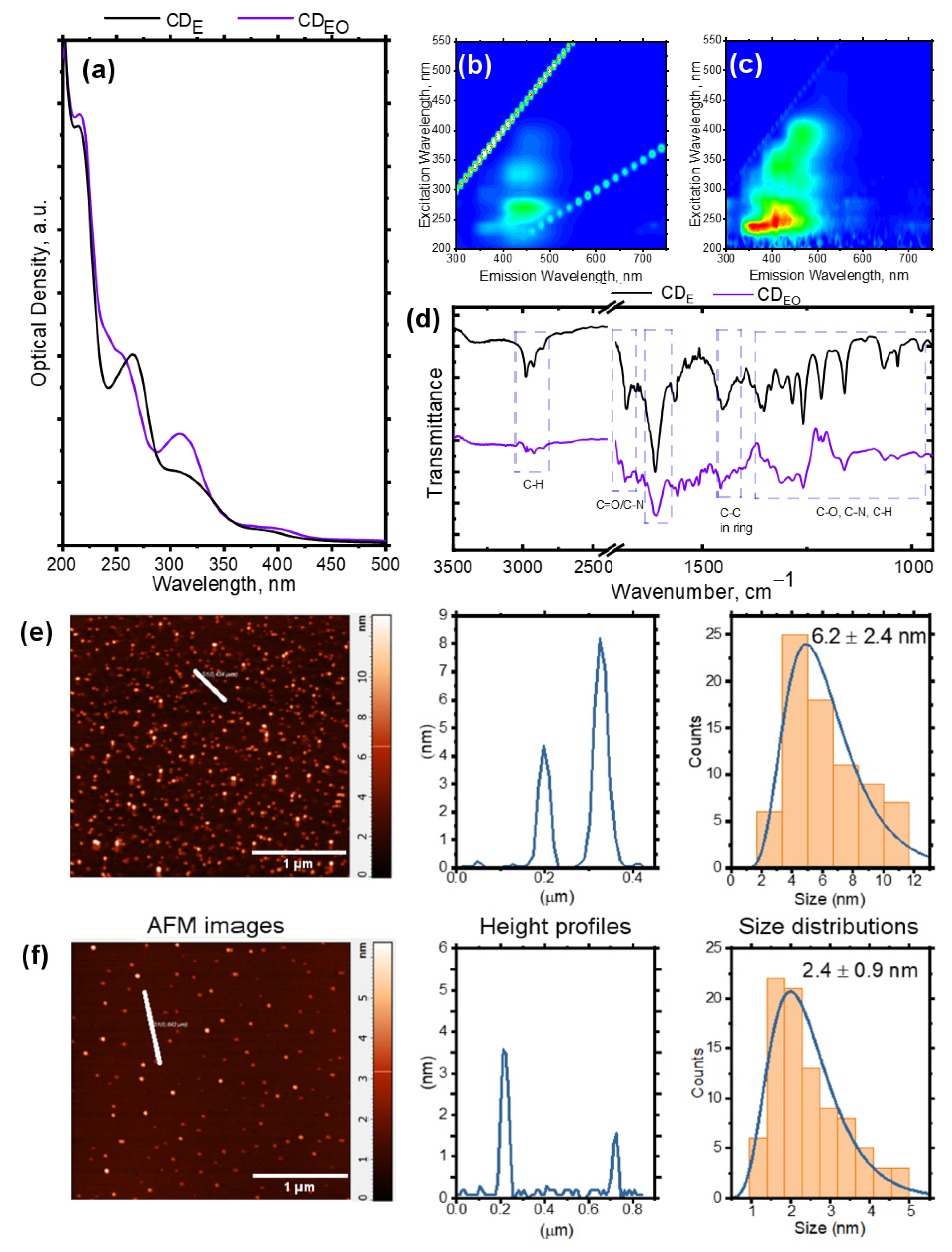
2.3. Characterization
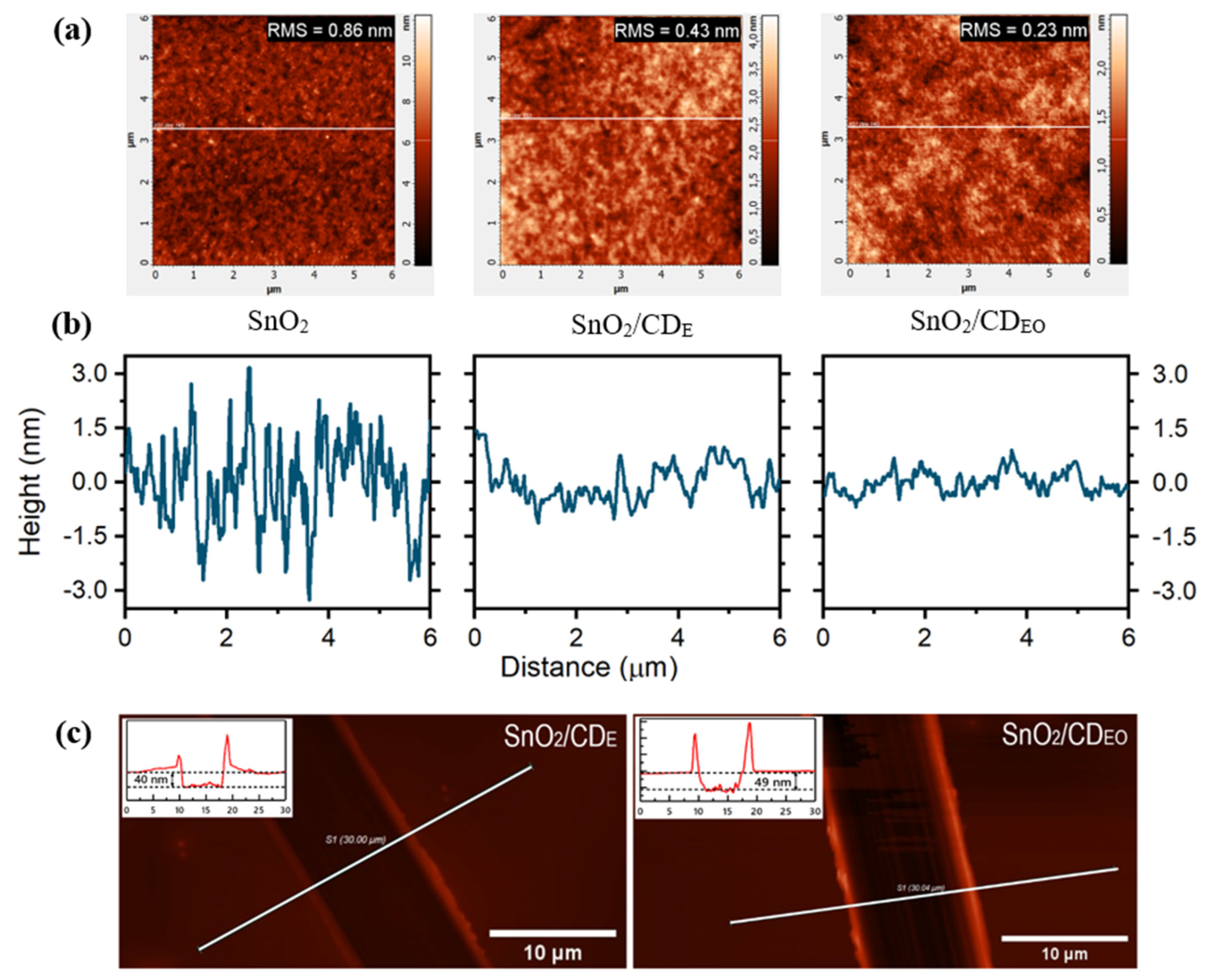
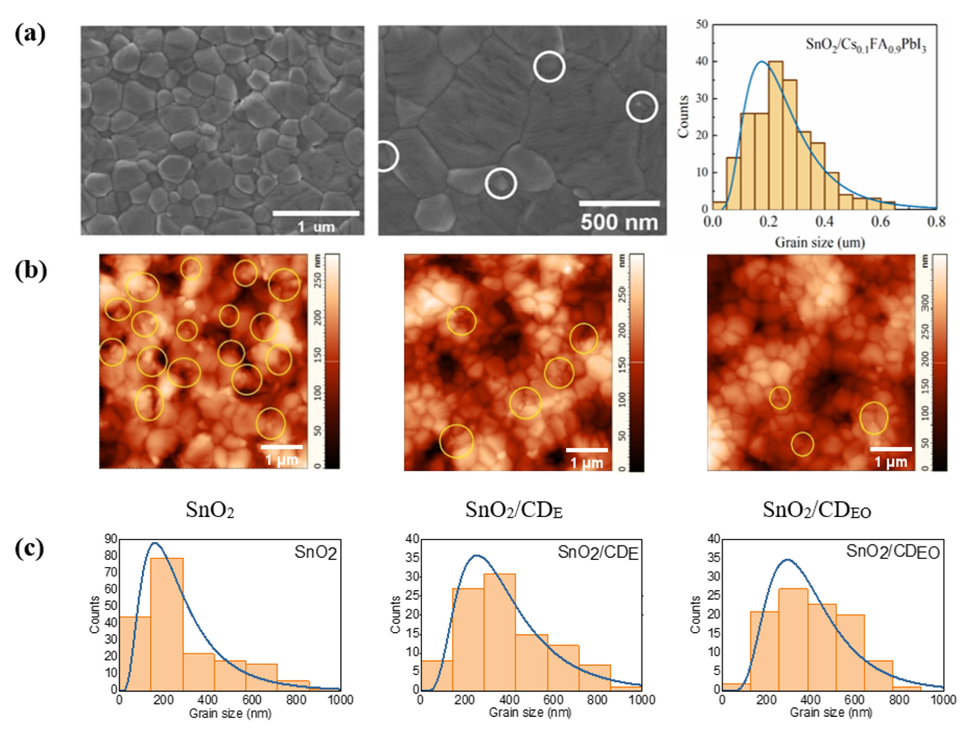
3. Results
4. Discussion
5. Conclusions
Author Contributions
Funding
Institutional Review Board Statement
Informed Consent Statement
Data Availability Statement
Acknowledgments
Conflicts of Interest
References
- Ellabban, O.; Haitham, A.R.; Frede, B. Renewable energy resources: Current status, future prospects and their enabling technology. Ren. Sustain. Energy Rev. 2014, 32, 748–764. [Google Scholar] [CrossRef]
- Peake, S. Renewable Energy-Power for a Sustainable Future; No. Ed. 4; Oxford University Press: Oxford, UK, 2018. [Google Scholar]
- Balakrishnan, P.; Shabbir, P.S.; Siddiqi, M.F.A.; Wang, X. Current status and future prospects of renewable energy: A case study. Energy Sources Part A Recovery Util. Environ. Effects 2020, 42, 2698–2703. [Google Scholar] [CrossRef]
- Gribov, B.G.; Zinov’Ev, K.V. Preparation of high-purity silicon for solar cells. Inorg. Mat. 2003, 39, 653–662. [Google Scholar] [CrossRef]
- Ranjan, S.; Balaji, S.; Panella, R.A.; Ydstie, B.E. Silicon solar cell production. Comp. Chem. Eng. 2011, 35, 1439–1453. [Google Scholar] [CrossRef]
- Xia, J.; Liang, C.; Gu, H.; Mei, S.; Li, S.; Zhang, N.; Xing, G. Surface passivation toward efficient and stable perovskite solar cells. Energy Environ. Mat. 2023, 6, e12296. [Google Scholar] [CrossRef]
- Lee, D.K.; Park, N.G. Additive engineering for highly efficient and stable perovskite solar cells. Appl. Phys. Rev. 2023, 10, 011308. [Google Scholar] [CrossRef]
- Kong, L.; Zhang, X.; Zhang, C.; Wang, L.; Wang, S.; Cao, F.; Yang, X. Stability of Perovskite Light-Emitting Diodes: Existing Issues and Mitigation Strategies Related to Both Material and Device Aspects. Adv. Mater. 2022, 34, 2205217. [Google Scholar] [CrossRef] [PubMed]
- Wei, K.; Liang, B.; Sun, C.; Jiang, Y.; Yuan, M. Metal Halide Perovskites for Red-Emission Light-Emitting Diodes. Small Struct. 2022, 3, 2200063. [Google Scholar] [CrossRef]
- Dong, H.; Zhang, C.; Liu, X.; Yao, J.; Zhao, Y.S. Materials chemistry and engineering in metal halide perovskite lasers. Chem. Soc. Rev. 2020, 49, 951–982. [Google Scholar] [CrossRef]
- Liu, M.; Grandhi, G.K.; Matta, S.; Mokurala, K.; Litvin, A.; Russo, S.; Vivo, P. Halide perovskite nanocrystal emitters. Adv. Photon. Res. 2021, 2, 2000118. [Google Scholar] [CrossRef]
- Cheng, P.; Han, K.; Chen, J. Recent Advances in Lead-Free Halide Perovskites for Photocatalysis. ACS Mater. Lett. 2022, 5, 60–78. [Google Scholar] [CrossRef]
- Wang, J.; Shi, Y.; Wang, Y.; Li, Z. Rational design of metal halide perovskite nanocrystals for photocatalytic CO2 reduction: Recent advances, challenges, and prospects. ACS Energy Lett. 2022, 7, 2043–2059. [Google Scholar] [CrossRef]
- Zhu, Y.; Liu, Y.; Miller, K.A.; Zhu, H.; Egap, E. Lead halide perovskite nanocrystals as photocatalysts for PET-RAFT polymerization under visible and near-infrared irradiation. ACS Macro Lett. 2020, 9, 725–730. [Google Scholar] [CrossRef] [PubMed]
- Zhu, Y.; Liu, Y.; Ai, Q.; Gao, G.; Yuan, L.; Fang, Q.; Lou, J. In situ synthesis of lead-free halide perovskite–COF nanocomposites as photocatalysts for photoinduced polymerization in both organic and aqueous phases. ACS Mater. Lett. 2022, 4, 464–471. [Google Scholar] [CrossRef]
- Furasova, A.; Voroshilov, P.; Sapori, D.; Ladutenko, K.; Barettin, D.; Zakhidov, A.; Makarov, S. Nanophotonics for perovskite solar cells. Adv. Photon. Res. 2022, 3, 2100326. [Google Scholar] [CrossRef]
- Chen, J.; Zhang, W.; Pullerits, T. Two-photon absorption in halide perovskites and their applications. Mater. Horiz. 2022, 9, 2255–2287. [Google Scholar] [CrossRef]
- Skurlov, I.D.; Yin, W.; Ismagilov, A.O.; Tcypkin, A.N.; Hua, H.; Wang, H.; Zheng, W. Improved one-and multiple-photon excited photoluminescence from Cd2+-doped CsPbBr3 perovskite NCs. Nanomaterials 2022, 12, 151. [Google Scholar] [CrossRef] [PubMed]
- Shen, W.; Chen, J.; Wu, J.; Li, X.; Zeng, H. Nonlinear optics in lead halide perovskites: Mechanisms and applications. ACS Photon. 2020, 8, 113–124. [Google Scholar] [CrossRef]
- Sokolova, A.V.; Tepliakov, N.V.; Ismagilov, A.O.; Tatarinov, D.A.; Kalinichev, A.A.; Koroleva, A.V.; Litvin, A.P. Stoichiometry Control in Dual-Band Emitting Yb3+-Doped CsPbCl x Br3–x Perovskite Nanocrystals. J. Phys. Chem. C 2022, 126, 20550–20557. [Google Scholar] [CrossRef]
- Wang, X.; Wang, Y.; Gao, W.; Song, L.; Ran, C.; Chen, Y.; Huang, W. Polarization-Sensitive Halide Perovskites for Polarized Luminescence and Detection: Recent Advances and Perspectives. Adv. Mater. 2021, 33, 2003615. [Google Scholar] [CrossRef]
- Miao, J.; Zhang, F. Recent progress on highly sensitive perovskite photodetectors. J. Mater. Chem. C 2019, 7, 1741–1791. [Google Scholar] [CrossRef]
- Mahapatra, A.S.; Kumar, P.; Kumar, P.; Pradhan, B. Recent progress in perovskite solar cells: Challenges from efficiency to stability. Mater. Today Chem. 2022, 23, 100686. [Google Scholar] [CrossRef]
- Basumatary, P.; Pratima, A. A short review on progress in perovskite solar cells. Mater. Res. Bull. 2022, 149, 111700. [Google Scholar] [CrossRef]
- Xia, C.; Peng, Q.; Poncé, J.; Patel, S.; Wright, J.B. Limits to electrical mobility in lead-halide perovskite semiconductors. J. Phys. Chem. Lett. 2021, 12, 3607–3617. [Google Scholar] [CrossRef] [PubMed]
- Herz, L.M. Charge-carrier mobilities in metal halide perovskites: Fundamental mechanisms and limits. ACS Energy Lett. 2017, 2, 1539–1548. [Google Scholar] [CrossRef] [Green Version]
- Liang, C.; Zhao, D.; Li, P.; Wu, B.; Gu, H.; Zhang, J. Simultaneously boost diffusion length and stability of perovskite for high performance solar cells. Nano Energy 2019, 59, 721–729. [Google Scholar] [CrossRef]
- Yang, Z.; Yu, Z.; Wei, H.; Xiao, X.; Ni, Z.; Chen, B. Enhancing electron diffusion length in narrow-bandgap perovskites for efficient monolithic perovskite tandem solar cells. Nat. Commun. 2019, 10, 4498. [Google Scholar] [CrossRef] [PubMed] [Green Version]
- Crespo, C.T. Absorption coefficients data of lead iodine perovskites using 14 different organic cations. Data Brief 2019, 27. [Google Scholar] [CrossRef] [Green Version]
- Faridi, A.W.; Imran, M.; Tariq, G.H.; Ullah, S.; Noor, S.F.; Ansar, S.; Sher, F. Synthesis and characterization of high-efficiency halide perovskite nanomaterials for light-absorbing applications. Ind. Eng. Chem. Res. 2022, 62, 4494–4502. [Google Scholar] [CrossRef]
- Hu, Z.; Lin, Z.; Su, J.; Zhang, J.; Chang, J.; Hao, Y. A review on energy band-gap engineering for perovskite photovoltaics. Solar Rrl. Solar Rrl. 2019, 3, 1900304. [Google Scholar] [CrossRef]
- Tao, S.X.; Xi, C.; Bobbert, P.A. Accurate and efficient band gap predictions of metal halide perovskites using the DFT-1/2 method: GW accuracy with DFT expense. Sci. Rep. 2017, 7, 14386. [Google Scholar] [CrossRef] [PubMed] [Green Version]
- Pachori, S.; Kumari, S.; Verma, A.S. An emerging high performance photovoltaic device with mechanical stability constants of hybrid (HC(NH2)2PbI3) perovskite. J. Mater. Sci. Mater. Electron. 2020, 31, 18004–18017. [Google Scholar]
- Targhi, F.F.; Jalili, Y.S.; Kanjouri, F. MAPbI3 and FAPbI3 perovskites as solar cells: Case study on structural, electrical and optical properties. Res. Phys. 2018, 10, 616–627. [Google Scholar] [CrossRef]
- Cui, X.; Jin, J.; Tai, Q.; Yan, F. Recent Progress on the Phase Stabilization of FAPbI3 for High-Performance Perovskite Solar Cells. Solar RRL. 2022, 6, 2200497. [Google Scholar] [CrossRef]
- Masi, S.; Gualdrón-Reyes, A.F.; Mora-Sero, I. Stabilization of black perovskite phase in FAPbI3 and CsPbI3. ACS Energy Lett. 2020, 5, 1974–1985. [Google Scholar] [CrossRef]
- Liu, Y.; Akin, S.; Hinderhofer, A.; Eickemeyer, F.T.; Zhu, H.; Seo, J.Y. Stabilization of highly efficient and stable phase-pure FAPbI3 perovskite solar cells by molecularly tailored 2D-overlayers. Angew. Chem. Int. Ed. 2020, 59, 15688–15694. [Google Scholar] [CrossRef]
- Chen, R.; Wu, Y.; Wang, Y.; Xu, R.; He, R.; Fan, Y. Crown Ether-Assisted Growth and Scaling Up of FACsPbI3 Films for Efficient and Stable Perovskite Solar Modules. Adv. Funct. Mat. 2021, 31, 2008760. [Google Scholar] [CrossRef]
- Stranks, S.D.; Snaith, H.J. Metal-halide perovskites for photovoltaic and light-emitting devices. Nat. Nanotechnol. 2015, 10, 391–402. [Google Scholar] [CrossRef]
- Min, H.; Kim, M.; Lee, S.U.; Kim, H.; Kim, G.; Choi, K.; Seok, S.I. Efficient, stable solar cells by using inherent bandgap of α-phase formamidinium lead iodide. Science 2019, 366, 749–753. [Google Scholar] [CrossRef]
- Yang, D.; Yang, R.; Wang, K.; Wu, C.; Zhu, X.; Feng, J.; Liu, S. High efficiency planar-type perovskite solar cells with negligible hysteresis using EDTA-complexed SnO2. Nat. Commun. 2018, 9, 3239. [Google Scholar] [CrossRef] [Green Version]
- Yang, L.; Zhou, H.; Duan, Y.; Wu, M.; He, K.; Li, Y. 24.96%-Efficiency FACsPbI3 Perovskite Solar Cells Enabled by Intermolecular Esterification Reaction of DL-Carnitine Hydrochloride. Adv. Mat. 2023, 25, 2211545. [Google Scholar] [CrossRef]
- Thote, A.; Jeon, I.; Lee, J.W.; Seo, S.; Lin, H.S.; Yang, Y. Stable and reproducible 2D/3D formamidinium–lead–iodide perovskite solar cells. ACS Appl. Energy Mater. 2019, 2, 2486–2493. [Google Scholar] [CrossRef]
- Liu, J.; Rui, L.; Bai, Y. Carbon dots: A new type of carbon-based nanomaterial with wide applications. ACS Central Sci. 2020, 6, 2179–2195. [Google Scholar] [CrossRef] [PubMed]
- Cui, L.; Ren, X.; Sun, M.; Liu, H.; Xia, L. Carbon dots: Synthesis, properties, and applications. Nanomaterials. 2021, 11, 3419. [Google Scholar] [CrossRef] [PubMed]
- Litvin, A.P.; Zhang, X.; Berwick, K.; Fedorov, A.V.; Zheng, W.; Baranov, A.V. Carbon-based interlayers in perovskite solar cells. Renew. Sustain. Energy Rev. 2020, 124, 109774. [Google Scholar] [CrossRef]
- Litvin, A.P.; Zhang, X.; Ushakova, E.V.; Rogach, A.L. Carbon Nanoparticles as Versatile Auxiliary Components of Perovskite-Based Optoelectronic Devices. Adv. Funct. Mater. 2021, 31, 2010768. [Google Scholar] [CrossRef]
- Stepanidenko, E.A.; Ushakova, E.V.; Fedorov, A.V.; Rogach, A.L. Applications of carbon dots in optoelectronics. Nanomaterials 2021, 11, 364. [Google Scholar] [CrossRef]
- Yadeta, T.F.; Huang, K.W.; Imae, T.; Tung, Y.L. Enhancement of Perovskite Solar Cells by TiO2-Carbon Dot Electron Transport Film Layers. Nanomaterials 2022, 13, 186. [Google Scholar] [CrossRef]
- Alkahtani, M.; Alenzi, S.M.; Alsolami, A.; Alsofyani, N.; Alfahd, A.; Alzahrani, Y.A.; Abduljawad, M. High-Performance and Stable Perovskite Solar Cells Using Carbon Quantum Dots and Upconversion Nanoparticles. Int. J. Mol. Sci. 2022, 23, 14441. [Google Scholar] [CrossRef]
- Zhang, X.; Zeng, Q.; Xiong, Y.; Ji, T.; Wang, C.; Shen, X.; Zheng, W. Energy level modification with carbon dot interlayers enables efficient perovskite solar cells and quantum dot based light-emitting diodes. Adv. Funct. Mater. 2020, 30, 1910530. [Google Scholar] [CrossRef]
- Ma, Y.; Zhang, H.; Zhang, Y.; Hu, R.; Jiang, M.; Zhang, R. Enhancing the performance of inverted perovskite solar cells via grain boundary passivation with carbon quantum dots. ACS Appl. Mat. Interf. 2018, 11, 3044–3052. [Google Scholar] [CrossRef]
- Ma, Y.; Zhang, H.; Zhang, Y.; Hu, R.; Jiang, M.; Zhang, R. Surface passivation with nitrogen-doped carbon dots for improved perovskite solar cell performance. J. Mater. Sci. 2018, 53, 9180–9190. [Google Scholar]
- Fang, X.; Ding, J.; Yuan, N.; Sun, P.; Lv, M.; Ding, G.; Zhu, C. Graphene quantum dot incorporated perovskite films: Passivating grain boundaries and facilitating electron extraction. Phys. Chem. Chem. Phys. 2017, 19, 6057–6063. [Google Scholar] [CrossRef] [PubMed]
- Wen, Y.; Zhu, G.; Shao, Y. Improving the power conversion efficiency of perovskite solar cells by adding carbon quantum dots. J. Mater. Sci. 2020, 55, 2937–2946. [Google Scholar] [CrossRef]
- Sánchez-Godoy, H.E.; Erazo, E.A.; Gualdrón-Reyes, A.F.; Khan, A.H.; Agouram, S.; Barea, E.M.; Mora-Seró, I. Preferred growth direction by PbS nanoplatelets preserves perovskite infrared light harvesting for stable, reproducible, and efficient solar cells. Adv. Energy Mater. 2020, 10, 2002422. [Google Scholar] [CrossRef]
- Parfenov, P.S.; Litvin, A.P.; Ushakova, E.V.; Fedorov, A.V.; Baranov, A.V.; Berwick, K. Note: Near infrared spectral and transient measurements of PbS quantum dots luminescence. Rev. Sci. Instrum. 2013, 84, 116104. [Google Scholar] [CrossRef] [PubMed]
- Xiang, Z.; Jiang, Y.; Cui, C.; Luo, Y.; Peng, Z. Sensitive, Selective and Reliable Detection of Fe3+ in Lake Water via Carbon Dots-Based Fluorescence Assay. Molecules 2022, 27, 6749. [Google Scholar] [CrossRef]
- Wang, B.; Wei, Z.; Sui, L.; Yu, J.; Zhang, B.; Wang, X.; Lu, S. Electron–phonon coupling-assisted universal red luminescence of o-phenylenediamine-based carbon dots. Light Sci. Appl. 2022, 11, 172. [Google Scholar] [CrossRef]
- Channa, A.M.; Siyal, A.N.; Memon, S.Q.; Parveen, S. Design of experiment for treatment of arsenic-contaminated water using Schiff’s base metal complex modified Amberlite XAD-2. Desalin. Water Treat. 2016, 57, 3664–3673. [Google Scholar] [CrossRef]
- Dong, W.; Zhang, X.; Yang, F.; Zeng, Q.; Yin, W.; Zhang, W.; Zheng, W. Amine-terminated carbon dots linking hole transport layer and vertically oriented quasi-2D perovskites through hydrogen bonds enable efficient LEDs. ACS Nano 2022, 16, 9679–9690. [Google Scholar] [CrossRef]
- Liu, B.T.; Zhang, Y.Z.; Zuo, Y.Y.; Rachmawati, D. Passivation and energy-level change of the SnO2 electron transport layer by reactive titania for perovskite solar cells. J. Alloys Compd. 2022, 929, 167349. [Google Scholar] [CrossRef]
- Huang, S.K.; Wang, Y.C.; Ke, W.C.; Kao, Y.T.; She, N.Z.; Li, J.X.; Chen, C.W. Unravelling the origin of the photocarrier dynamics of fullerene-derivative passivation of SnO2 electron transporters in perovskite solar cells. J. Mater. Chem. A 2020, 8, 23607–23616. [Google Scholar] [CrossRef]
- Zhu, Z.; Ma, J.; Wang, Z.; Mu, C.; Fan, Z.; Du, L.; Yang, S. Efficiency enhancement of perovskite solar cells through fast electron extraction: The role of graphene quantum dots. J. Am. Chem. Soc. 2014, 136, 3760–3763. [Google Scholar] [CrossRef] [PubMed]
- Kulbak, M.; Gupta, S.; Kedem, N.; Levine, I.; Bendikov, T.; Hodes, G.; Cahen, D. Cesium enhances long-term stability of lead bromide perovskite-based solar cells. J. Phys. Chem. Lett. 2016, 7, 167–172. [Google Scholar] [CrossRef] [Green Version]
- Benetti, D.; Jokar, E.; Yu, C.H.; Fathi, A.; Zhao, H.; Vomiero, A.; Rosei, F. Hole-extraction and photostability enhancement in highly efficient inverted perovskite solar cells through carbon dot-based hybrid material. Nano Energy 2019, 62, 781–790. [Google Scholar] [CrossRef]
- Gan, X.; Yang, S.; Zhang, J.; Wang, G.; He, P.; Sun, H.; Zhu, Y. Graphite-N doped graphene quantum dots as semiconductor additive in perovskite solar cells. ACS Appl. Mater. Interf. 2019, 11, 37796–37803. [Google Scholar] [CrossRef]
- Kirbiyik, C.; Toprak, A.; Baslak, C.; Kus, M.; Ersoz, M. Nitrogen-doped CQDs to enhance the power conversion efficiency of perovskite solar cells via surface passivation. J. Alloys Compd. 2020, 832, 154897. [Google Scholar] [CrossRef]
- Yeh, T.F.; Teng, C.Y.; Chen, S.J.; Teng, H. Nitrogen-doped graphene oxide quantum dots as photocatalysts for overall water-splitting under visible light Illumination. Adv. Mater. 2014, 26, 3297–3303. [Google Scholar] [CrossRef]


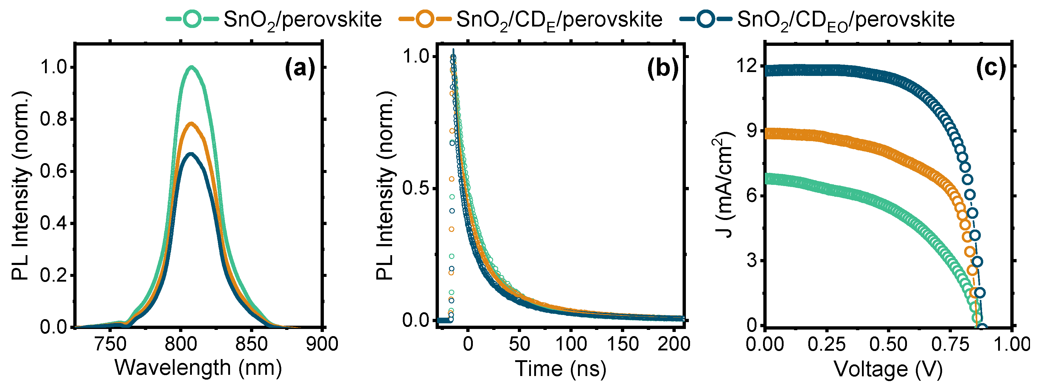
| Τavg (ns) | A1 | (ns) | A2 | (ns) | A3 | (ns) | |
|---|---|---|---|---|---|---|---|
| SnO2/Perovskite | 26.5 | 0.09 | 10.4 | 0.35 | 27.3 | 0.06 | 94.6 |
| SnO2/CDE/Perovskite | 21.9 | 0.03 | 6.4 | 0.29 | 22.1 | 0.12 | 75.7 |
| SnO2/CDEO/Perovskite | 20.8 | 0.04 | 5.8 | 0.24 | 21.1 | 0.09 | 82.0 |
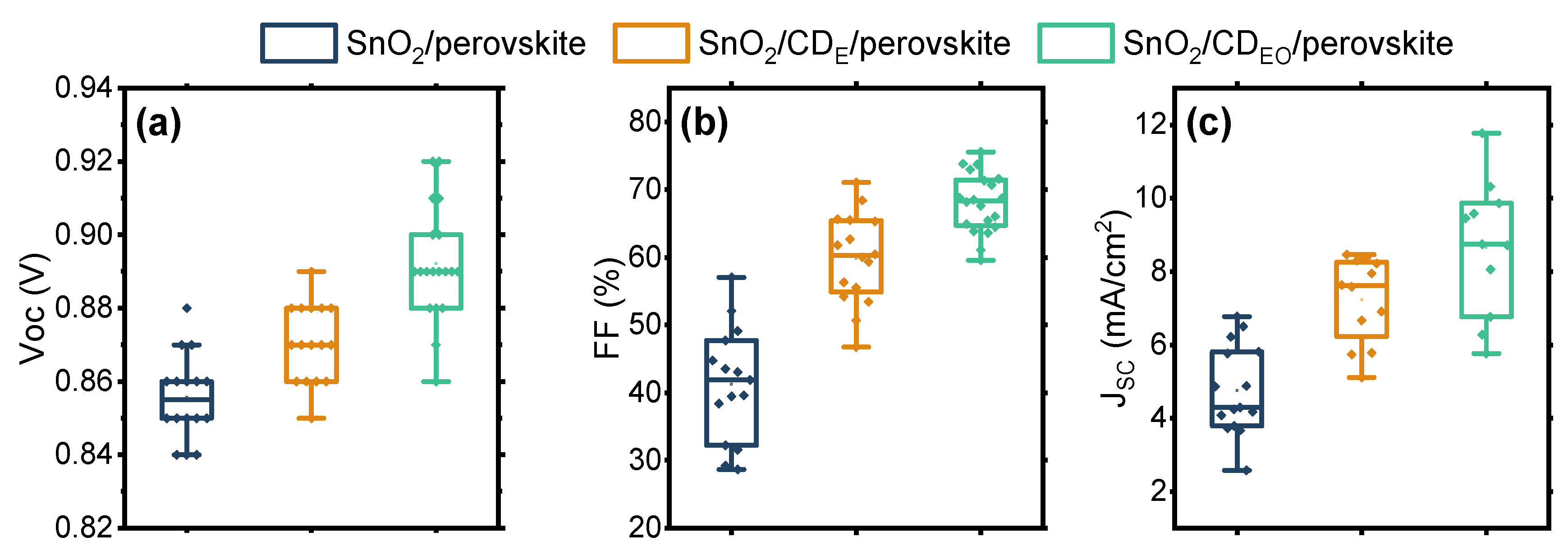
| Name | Voc (V) | Jsc (mA/cm2) | FF, % | PCE, % | |
|---|---|---|---|---|---|
| CD-free | Average | 0.86 ± 0.01 | 4.8 ± 1.2 | 41 ± 8 | 1.9 ± 0.6 |
| Champion | 0.88 | 6.8 | 57 | 2.9 | |
| CDE interlayer | Average | 0.87 ± 0.01 | 7.2 ± 1.2 | 60 ± 7 | 3.8 ± 0.5 |
| Champion | 0.89 | 8.5 | 71 | 4.8 | |
| CDEO interlayer | Average | 0.89 ± 0.02 | 8.7 ± 1.8 | 68 ± 4 | 5.0 ± 1.1 |
| Champion | 0.92 | 11.8 | 76 | 6.9 |
Disclaimer/Publisher’s Note: The statements, opinions and data contained in all publications are solely those of the individual author(s) and contributor(s) and not of MDPI and/or the editor(s). MDPI and/or the editor(s) disclaim responsibility for any injury to people or property resulting from any ideas, methods, instructions or products referred to in the content. |
© 2023 by the authors. Licensee MDPI, Basel, Switzerland. This article is an open access article distributed under the terms and conditions of the Creative Commons Attribution (CC BY) license (https://creativecommons.org/licenses/by/4.0/).
Share and Cite
Margaryan, I.V.; Vedernikova, A.A.; Parfenov, P.S.; Baranov, M.A.; Danilov, D.V.; Koroleva, A.V.; Zhizhin, E.V.; Cherevkov, S.A.; Zhang, X.; Ushakova, E.V.; et al. An Interlayer of Ultrasmall N-Rich Carbon Dots for Optimization of SnO2/CsFAPbI3 Interface. Photonics 2023, 10, 379. https://doi.org/10.3390/photonics10040379
Margaryan IV, Vedernikova AA, Parfenov PS, Baranov MA, Danilov DV, Koroleva AV, Zhizhin EV, Cherevkov SA, Zhang X, Ushakova EV, et al. An Interlayer of Ultrasmall N-Rich Carbon Dots for Optimization of SnO2/CsFAPbI3 Interface. Photonics. 2023; 10(4):379. https://doi.org/10.3390/photonics10040379
Chicago/Turabian StyleMargaryan, Igor V., Anna A. Vedernikova, Peter S. Parfenov, Mikhail A. Baranov, Denis V. Danilov, Aleksandra V. Koroleva, Evgeniy V. Zhizhin, Sergey A. Cherevkov, Xiaoyu Zhang, Elena V. Ushakova, and et al. 2023. "An Interlayer of Ultrasmall N-Rich Carbon Dots for Optimization of SnO2/CsFAPbI3 Interface" Photonics 10, no. 4: 379. https://doi.org/10.3390/photonics10040379