Bandwidth Expansion of Zero-Power-Consumption Visible Light Communication System


1
Key Laboratory of Opto-Electronic Materials and Devices, Institute of Semiconductors, Chinese Academy of Sciences, Beijing 100083, China
2
College of Materials Science and Opto-Electronic Technology, University of Chinese Academy of Sciences, Beijing 100049, China
3
School of Electronic, Electrical and Communication Engineering, University of Chinese Academy of Sciences, Beijing 101408, China
*
Author to whom correspondence should be addressed.
Photonics 2023, 10(4), 376; https://doi.org/10.3390/photonics10040376
Submission received: 13 February 2023
/
Revised: 21 March 2023
/
Accepted: 22 March 2023
/
Published: 28 March 2023
(This article belongs to the Special Issue Visible Light Communications)
Abstract
:The data rate of the zero-power-consumption visible light communication system is limited due to the solar cell bandwidth limit. A new method has been proposed to improve the data rate of communication systems. The predistortion circuit based on the nonlinear compensation principle of the communication system is added between the transmitter and the receiver to equalize the amplitude–frequency response of the solar cell. Based on the measurement of the original amplitude–frequency response of the system, the zero-pole of the predistortion circuit is calculated, and an accurate equalization circuit is designed by using separate components to expand the 3 dB bandwidth of the system. The test results show that the 3 dB bandwidth of the visible light self-powered communication system is increased from 85 kHz to 750 kHz, and the system bandwidth is expanded by nearly 10 times.
1. Introduction
Visible light communication (VLC) is a promising communication technology combines the advantages of lighting and communication simultaneously. With high speed, large capacity, no need for spectrum authorization, possibly integrating into indoor lighting and other advantages, VLC has been rapidly developed in recent years. In terms of energy saving, a VLC system can be combined with the existing lighting network [1]. It can deploy communication networks with little energy consumption and expenditure. Currently, VLC based on photovoltaic (PV) devices are receiving more and more attention. Compared to the VLC system based on photoelectric detectors (PD), PV devices could collect the energy from the lighting source and supply energy to the receiver. When the energy provided by the PV device can meet the power consumption of the receiving device, the receiver can realize zero-power consumption communication without an external power supply. Zero-power-consumption VLC systems with a solar cell can greatly satisfy the requirements of some specific applications. These include enabling more Internet of Things (IoT) nodes to eliminate power cables and realize a more flexible deployment in large-capacity IoT applications. In 2013, Kim et al. proved that solar cells could detect variational optical signals under solar illumination, proving the feasibility of solar cells as detectors of an optical communication system [2]. In 2015, Chen et al. increased the communication rate of their system from 10 kbps to 400 kbps based on the digital equalization method [3], but the bandwidth was not indicated in that paper. In the same year, Malik et al. used solar cells to realize 8 kbps zero-power visible light communication [4]. In 2016, Carrascal et al. built an on-demand wake-up receiver with a 10 kHz bandwidth zero-power communication system [5]. In 2020, Sun et al. built a zero-power communication system with silicon solar cells and improved the communication rate by weak signal detection and a data reconstruction algorithm when the bandwidth was only 10 kHz [6]. From the existing research results, the communication rate of the zero-power-consumption VLC system is restricted by the system bandwidth, specifically, by the bandwidth of the solar cell. Compared with other high speed VLC systems, limited bandwidth and lower data rates limit the application and promotion of the zero-power-consumption VLC system.
In this paper, in order to improve the communication speed of this system, the reasons for the slow response speed of solar cells were analyzed based on the solar cell model. Moreover, the equalization circuit was designed by means of nonlinear compensation to expand the insufficient bandwidth of solar cell devices. The design idea of a predistortion equalization circuit for a zero-power-consumption VLC system is presented. This equalization circuit is different from the equalization circuit in the VLC system based on the PIN detector. It does not improve the response of the LED high-frequency signal with more than 3 dB bandwidth; rather, it improves the frequency response of a certain segment of the 3 dB bandwidth of the LED according to the frequency response characteristics of the solar cell at the receiver. In this paper, a design method of the equalization circuit parameters is proposed. Furthermore, the experimental test proved that the equalization circuit can effectively expand the bandwidth of the zero-power-consumption VLC system.
2. Model and Principle
2.1. Model of Zero-Power-Consumption VLC System
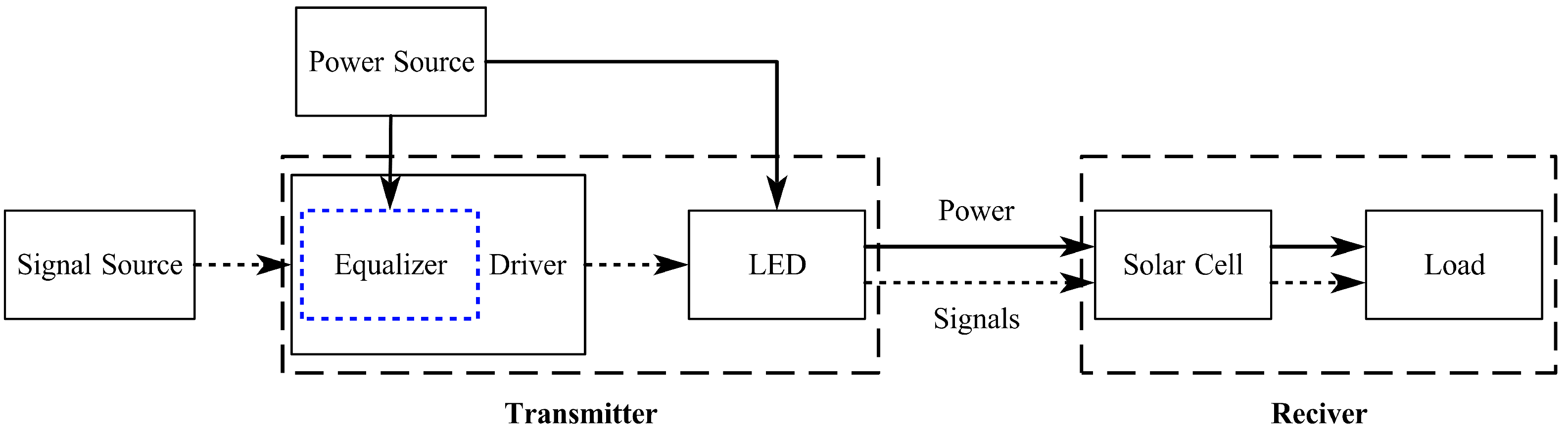
The zero-power-consumption VLC system includes signal source, power source, transmitter, air channel and receiver, as shown in Figure 1. The signal source puts the data into the system, and the power source supplies energy to the transmitter. The transmitter consists of an LED and its drive circuit. The drive circuit is used to load signals onto the LED lamp, and keep the lamp lighting. The drive circuit can work whether the equalizer is added or not. The receiver is made up of a solar cell and an external load. The solar cell acts as a detector that captures the light signal and a power supply of external loads, such as a low-power MCU. The receiver of the system could therefore realize zero power consumption.
In this VLC system, the LED lamp is used as the transmitter, and the light emitted by the LED lamp can be taken as an approximate Lambert radiant light source after astigmatism. The light power emitted by the LED lamp is . and are the lower limit and upper limit of the spectral components of the light source, and represents the radiation flux at a specific wavelength [7]. Furthermore, the optical antenna can affect the final light power passing through the lamp. Normally, the effect of the optical antenna is not significant.
The DC gain of optical signal in air channel is given by the Lambert light source model.
where m is the Lambert model order, , A is the surface area of the receiver, d is the linear distance between the light source and the detector, is the emission angle of the light source, is the receiving angle of the detector, which is approximately zero in the direct link where the distance is much larger than the size of the light source and the detector, is the gain of the optical filter and is the gain of the optical concentrator. The optical power obtained by the receiver is . When the emitting surface of the LED is placed parallel to the solar cell, the transmitting angle is equal to the receiving angle. Without the filter and concentrating lens, the optical filter gain and the optical concentrator gain are both 1. Finally, the optical power received by the system can be expressed as
2.2. Models of Solar Cell
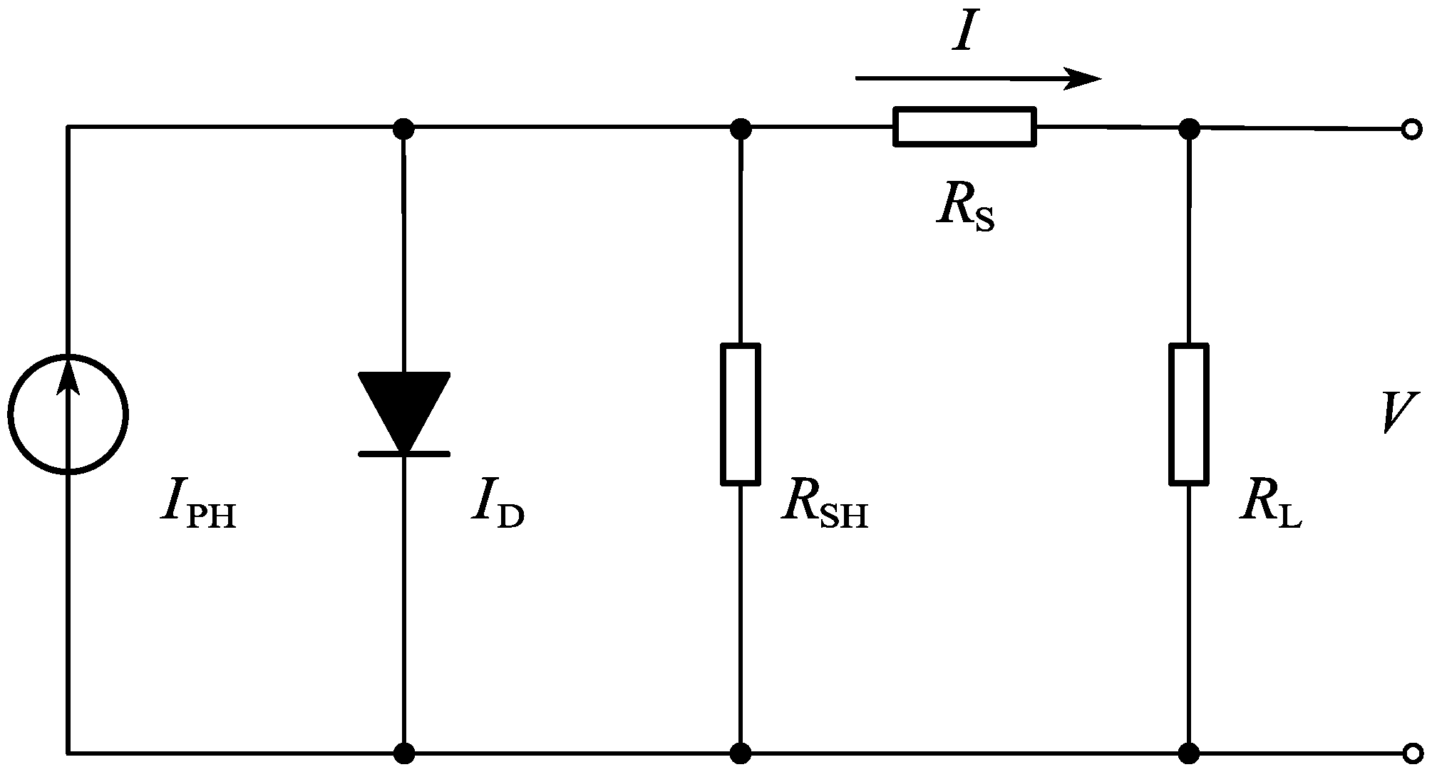
As the detector, the DC model of solar cell is shown in Figure 2.
In the figure, is the current generated by the solar cell under specific light, which is determined by the optical power received by the receiver, is the diode current describing the composite loss of the space charge zone in the solar cell, related to temperature T, diode ideal factor A and the number of arrays in series N . k is the Boltzmann constant, and is the saturation dark current, which is usually negligible compared to the exponential terms. is the shunt resistance of the leakage current of the solar cell, and is the equivalent resistance in series that causes voltage loss on the connection lines between different cells. is the load resistance connected to the port of solar cell. The value of the affects the power output of the solar cell. The proper and can be obtained by testing the volt–ampere characteristic curves of solar cell, and it is considered that the range of illumination remains constant.
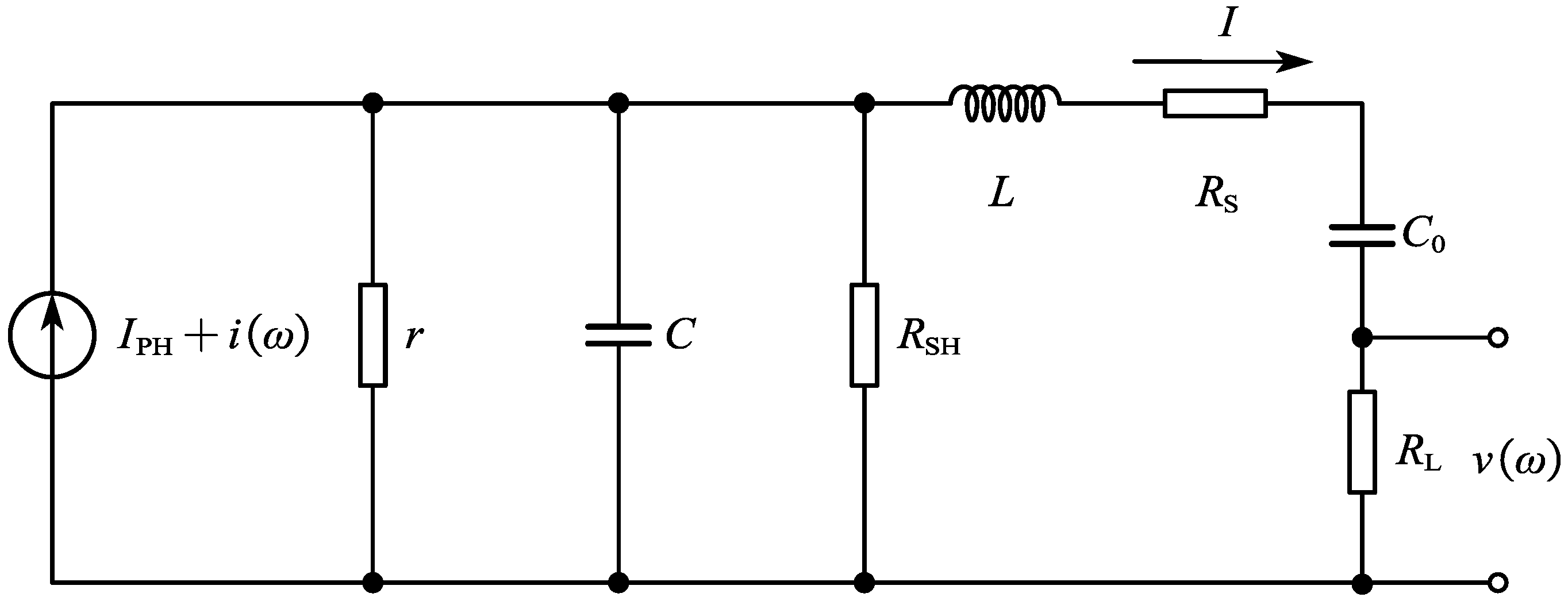
Under the condition of an AC signal, the equivalent model is shown in Figure 3. The diode in the DC model is represented as the equivalent resistance of the diode with a small signal. is the DC isolation capacitor. The larger the value of it, the less of the low-frequency component loss and the DC drift [7].
is the photocurrent generated by the solar cell from the received signal, C is the junction capacitance of the solar cell and L is the equivalent inductance introduced by all the connecting lines in the solar cell. From this model the amplitude–frequency response could be calculated by
It can be seen that C of the solar cell leads to a large attenuation of amplitude–frequency response at high frequency. Due to the large area of the solar cell, its capacitance value is usually much larger than that of the PIN detector. As the result, the RC constant of solar cells is large and the response time is slow.
2.3. Principles of Equalization Circuit Design
The bandwidth of the system can be determined by the frequency response. The low bandwidth of the system causes the attenuation of high-frequency signals and prevents the symbol conversion within a clock cycle. A symbol extends to the neighboring symbol so that the integrity of the signal is damaged. The transmission rate of the symbol is limited [8]. The frequency response of a system is equal to the product of the frequency response of the cascaded circuits that the system consists of.
Each subscript represents different cascaded networks in the system. In a zero-power communication system, the frequency response of the system can be expressed as the multiplication of the transmitter and the receiver.
where is the frequency response of the transmitter, and is the frequency response of the receiver. In the zero-power-consumption VLC system using solar cells as detectors, the cutoff frequency of the LED is much higher than that of the solar cell, so the system bandwidth is mainly limited by the solar cell. In the low-frequency range the amplitude–frequency response of the LED is flat and the gain is basically constant until the frequency exceeds the LED cutoff frequency. The cutoff frequency of the system is limited by the frequency response of the solar cell. To improve the amplitude of the high-frequency response, an equalization circuit should be connected whose frequency response is “complementary’ to the unequalized system within a certain range of frequency. The frequency response of the equalizing circuit within that range is where K is the DC gain of the circuit. In the VLC system, the system bandwidth can be expanded and the reliability and stability can be improved by offsetting the signal attenuation of a specific frequency. An equalization circuit is a circuit that amplifies different frequency components of input signals in a differentiated manner. Its response to different frequency signals can be represented by the transfer function. The transfer function can be described by its magnitude and angle. The change of the magnitude with frequency is the amplitude–frequency response, and the change of the angle with frequency is the phase–frequency response. Intensity modulation is chosen in a VLC system, so that we pay more attention to the amplitude–frequency response. The amplitude–frequency response of the circuit can be determined by the zero-pole positions of the circuit transfer function. The curve of the transfer function can be determined when the position of the zero-pole is known. Furthermore, the expression of the transfer function depends on the certain circuit structure. Finally, an equalization circuit with appropriate amplitude–frequency response characteristics could be constructed by discrete components and compensate for the amplitude–frequency response of the VLC system.
3. System Design
3.1. Unequalized System
In order to build the high-speed zero-power-consumption VLC system, the power consumption and bandwidth of that system should be evaluated first. There are two approaches to test the system bandwidth. One is to use the vector network analyzer (VNA). The VNA sends out and receives the test signals passing through the VLC system from different ports. Another option is to use the signal generator and oscilloscope test manually. To perform the test, first adjust the signal generator output to the sinusoidal signals of different frequencies with a certain amplitude as the system input signal. Then, measure the amplitude of the system output signal with the oscilloscope, scan and record the amplitude–frequency response of the system. Which test method is chosen depends on the system bandwidth. The zero-power-consumption VLC system using solar cells as detectors is a low-speed system with limited bandwidth. The current VNA E5071B in our laboratory has a start frequency 300 kHz, which is much higher than the cutoff frequency of commercial solar cells. The method of using a VNA to measure the amplitude–frequency response of the system is no longer applicable in this case, so the low-frequency amplitude–frequency response of the unequalized system needs to be tested manually. When the components of the communication system are selected, the system bandwidth is determined as well. After the amplitude–frequency response test of the system, the ideal amplitude–frequency response of the equalization circuit can be calculated. The amplitude–frequency response of the proposed unequalized system is given in Section 4.1 as Figure 7 (black line) shows.
3.2. Equalization Circuit Design
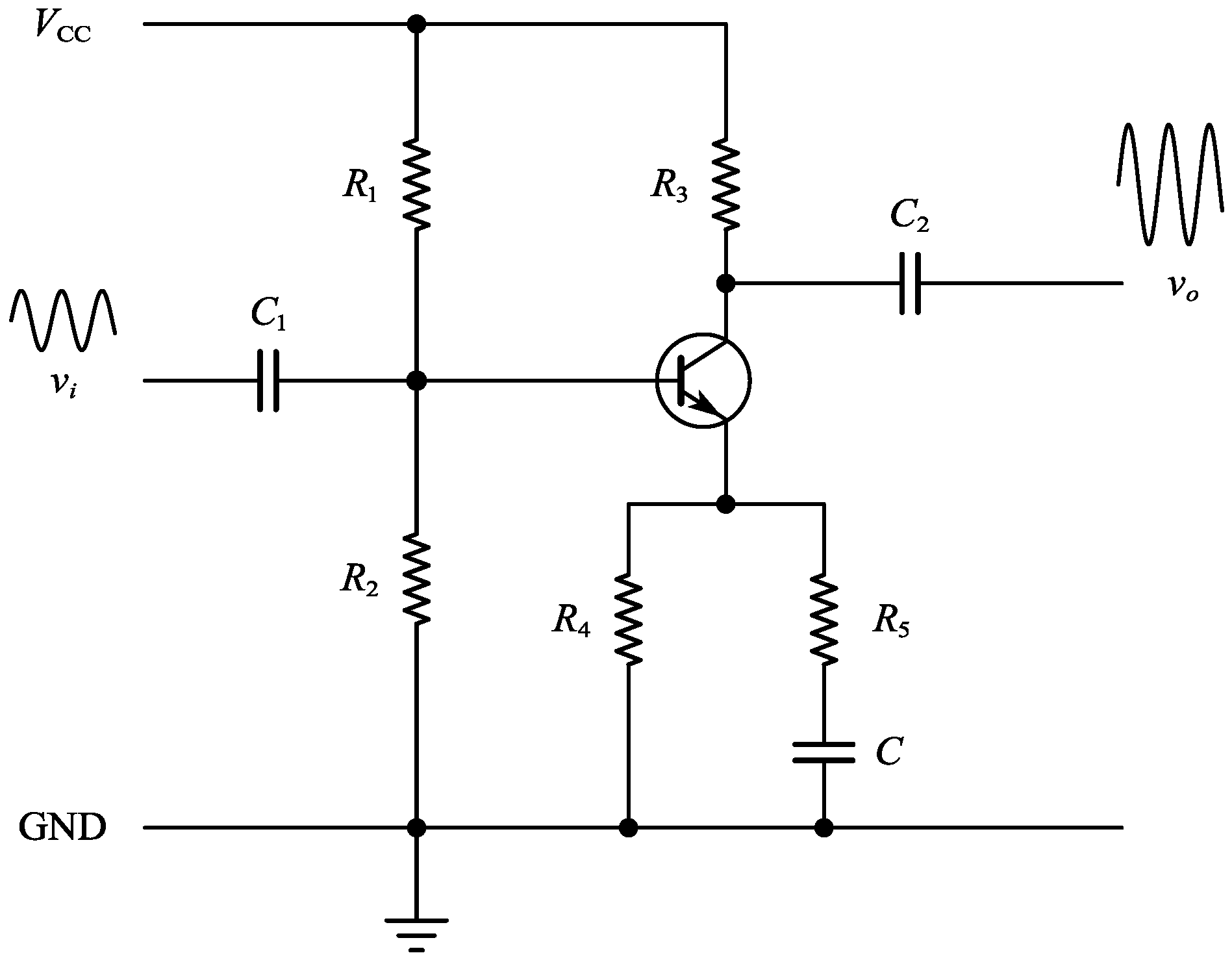
The amplitude–frequency response of the equalization circuit needs to be designed carefully. According to the principle of equalization, the frequency response of the circuit can be obtained from the known transfer function. The zero-pole of the transfer function can determine the transfer function curve, while the appropriate zero-pole of the transfer function curve can be obtained by Matlab. The value of a determined zero-pole can be achieved using different circuit structures. In order to reduce the complexity of the circuit, a first-order active amplifier is used to construct the equalization circuit. The structure of the designed active equalization circuit is shown in Figure 4.
In the above, and represent DC bias resistance. To determine the static operating point of the transistor, it is necessary to determine the resistance value according to the specific model of the transistor and the power supply voltage. and are DC isolation capacitors, used to isolate the DC components between the front and back circuits, reducing the complexity of circuit design. is the DC power supply that provides energy for amplifying the input signal. The input signal of the equalization circuit is , the output signal is and the transfer function is . According to the circuit structure, the expression of the transfer function and the zero-pole of the equalization circuit can be determined.
where K is a constant term, affecting the position of the system frequency response curve in the vertical direction without changing the shape of the curve, and this value can be explained as a gain component of the transfer function.
In the expression, is the input resistance of the later stage circuit, which is a determined value, in the case of matching impedance it can be selected as 50 Ω. The resistance value of can be determined according to the expression of K and the values of and . When , and C take appropriate values, the transfer function of the equalizer circuit shows the same curve as that obtained by software simulation. The frequency response of the circuit is when . Since the zero-pole of the circuit is derived from the ideal transfer function, it is almost the same as the ideal amplitude–frequency response.
4. Experiments and Tests
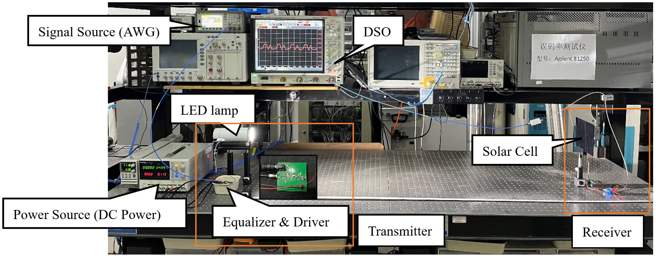
The bandwidth expansion performance test system is shown in Figure 5. In the experiment, an arbitrary waveform generator (AWG, Keysight 33600A) was used as the signal source, and it send signals to the equalization circuit and drive circuit. The equalizer and driver were printed in one PCB. A commercial high-power fluorescent white LED lamp was used as the light source, with electric power of 15 W, working current of 300 mA and a general rendering index of 90. The communication distance was 1.5 m. A CdTe solar cell (164 × 133 × 3.2 mm) was used as the detector, and an illumination meter (TES-1339) measured the average illumination at the receiver of 600 lx. The received signal waveform was observed using a Digital Storage Oscilloscope (DSO, Keysight DSOS204A). The amplitude of the signal was 200 mV, and the digital oscilloscope was set to AC coupling. The used transistor is a typical NPN transistor SS8050. The used MOSFET in the driver was model BSP297. was 5 V which was provided by DC power supply in the equalizer circuit, , , , , and , and all the test operations were under those parameters.
4.1. Amplitude–Frequency Response of the Transmitter
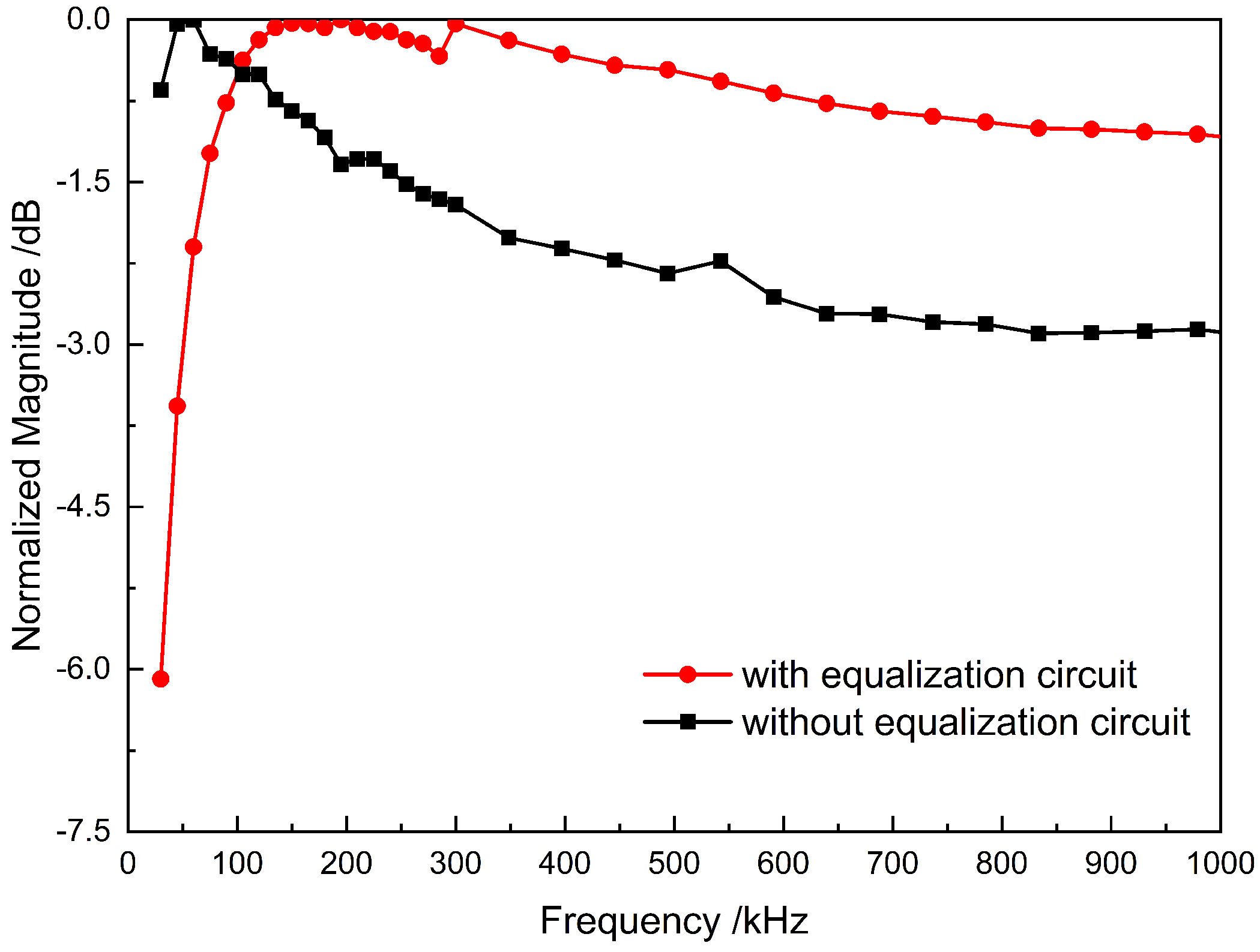
The bandwidth of the transmitter is smaller than the bandwidth of a commercial detector. When the receiver is a high-bandwidth commercial PIN detector, the system bandwidth is limited by the transmitter. According Figure 1, without the equalizer, the bandwidth of the transmitter is the bandwidth of the high-power LED lamp. As Figure 6 shows, the amplitude-to-frequency response of the LED is flat within 1 MHz (black line). The amplitude–frequency response of the transmitter is changed significantly when the equalization circuit is added, so the bandwidth is also changed. With the equalization circuit, the amplitude–frequency response of the transmitter is nonlinear and amplified within the low-frequency range. That is different from the traditional VLC system, which pursues a flat LED amplitude–frequency response. With the equalization circuit, the transmitter bandwidth is determined by both the equalization circuit and the LED lamp. The amplitude–frequency response of the transmitter is nonlinear lifted within 100 kHz (red line), and the response of the high-frequency part increases as well. Due to the presence of the DC isolation capacitor, the test starts at 30 kHz. As can be seen from the figure, the bandwidth of the transmitter is much higher than 1 MHz. However, the most important part of the zero-power-consumption VLC system amplitude–frequency response is the low-frequency.
The amplitude–frequency response of the transmitter compensated for the amplitude–frequency response of the receiver within the cutoff frequency of the system in Figure 7. In addition, the figure used a relative representation to show the result more clearly.
4.2. Amplitude–Frequency Response of the System
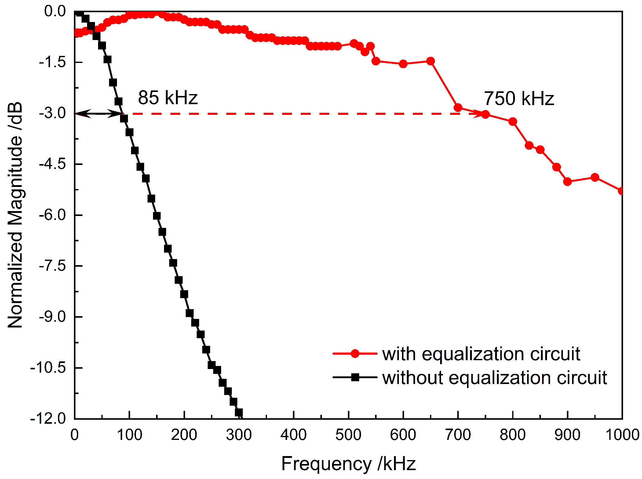
When the solar cell is used as the detector in the receiver, the test of frequency response is focused on the whole zero-power-consumption VLC system. The test frequency range was from 5 kHz to 1 MHz, and the result with the relative representation is shown in Figure 7.
Before the bandwidth expansion, the bandwidth of the zero-power-consumption VLC system was only 85 kHz. The received signals were too messy to build the eye diagram. After the bandwidth expansion, the bandwidth extended to 750 kHz. The bandwidth extended by about 10 times when the equalization circuit was used.
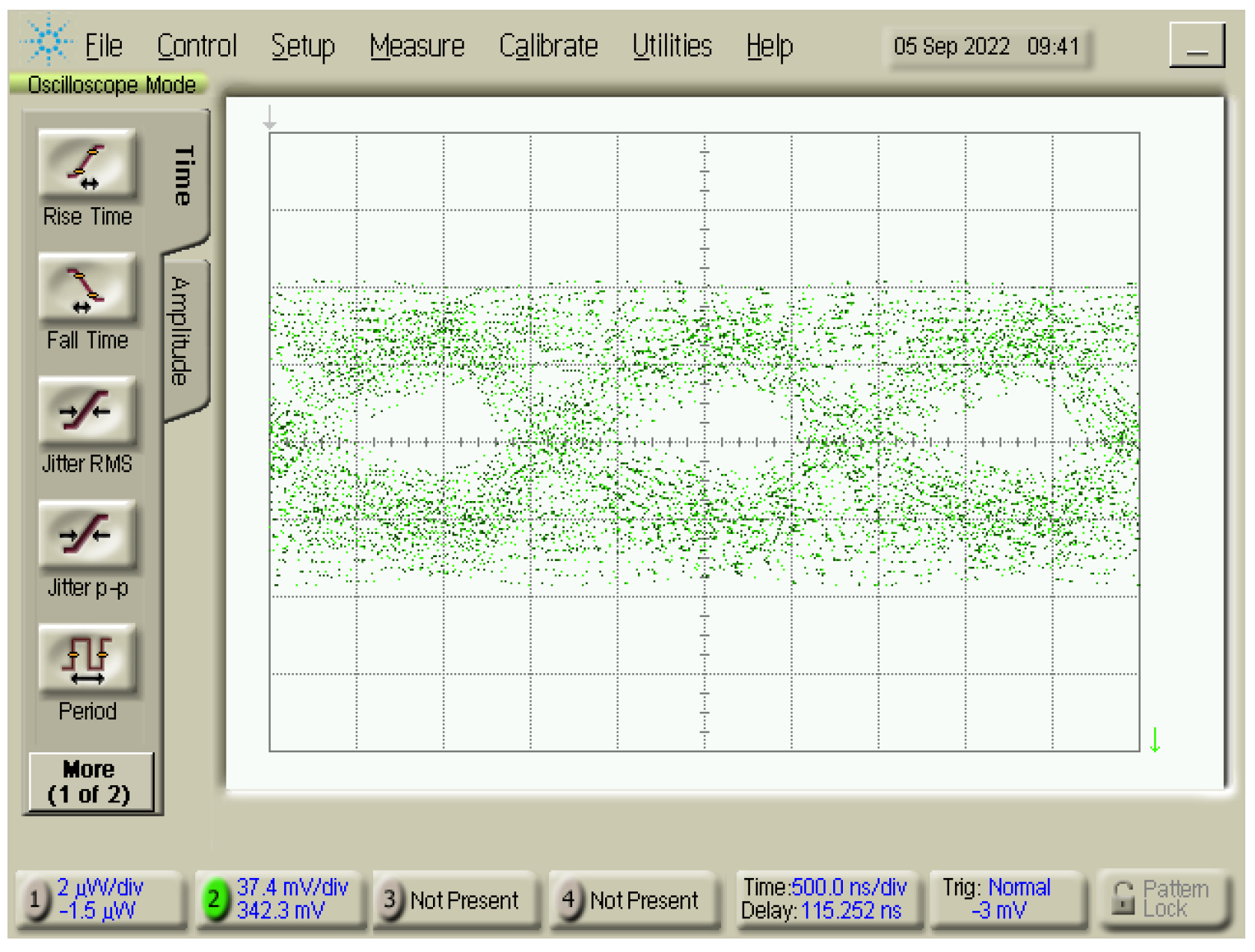
The eye diagram with 600 kbps pseudo-random sequence is shown in Figure 8. It shows that the system with the equalization circuit can achieve that data rate. The amplitude–frequency response of this system decreased slowly after 750 kHz, which means that higher order equalization circuits could be used to expand the bandwidth further. However, the complexity of the system will be increased. That means there is a trade-off between expanding the bandwidth range and system complexity. It is significant to select an appropriate equalization circuit structure and the corresponding component parameters according to the application demand.
5. Discussion
Improving the communication rate is a very important goal of the research of zero-power-consumption VLC system. There are two approaches to realize a higher data rate. One method is to improve the bandwidth utilization, as shown in [3]. One can adjust the rise and fall edge of the signal by digital predistortion to fit the certain channels. It was shown that the data rate increased from 10 kbps to 400 kbps in 75 cm distance, and the predistortion scheme needs to adapt to the bandwidth of the receiver specifically. Another method is to improve the bandwidth of the system. In [4,6], an active data processing circuit is added in the receiver. The signal is sampled and recovered by an active data processing circuit before sending to next stage. The circuit needs extra power consumption in order to make the received signal operable. In that method, the active data processing circuit increased the complexity of the receiver. Adding a bandwidth enhancement circuit (BEC) in the receiver is an effective method to expand the bandwidth of the system as well. In [9], the BEC is an active circuit, including an equalizer and non-inverting amplifier. The bandwidth expanded from 163 kHz to 1.62 MHz, so the great improvement of the bandwidth needed much more power from the receiver. In that paper, the power consumption of the BEC required even more power than the total power supplied from the solar cell. If there is no approach to increase the power that the solar cell supplies, the complex BEC cannot used to build a zero-power-consumption VLC system.
Compared with those existing methods, the bandwidth expansion method in this paper does not consume the extra power of the receiver. Setting the equalization circuit at the transmitter can save power at the receiver. All the energy of the receiver could be used. The power consumption of the equalizer is 460–470 mW in this system. Compared with the total power consumption of the system, 11.2 W, the equalizer power consumption is only 4.1% of the system. The equalizing circuit increases the complexity of the system, but the cost will not increase much because the transistor, resistor and capacitor are low-energy devices. The extra complexity and power consumption cost by using the equalization circuit is worth the increase in the system bandwidth and communication rate. Setting the circuit in the transmitter is a potential bandwidth expansion scheme in a zero-power-consumption VLC system, because there is no power consumption in the receiver. As Table 1 shows, with an equalization circuit in the transmitter, there is a good trade-off between bandwidth, complexity and power consumption, and it provides a higher speed data rate with enough distance. That means in a normal indoor lighting condition, this scheme can be used to build a communication system. Furthermore, these schemes can be combined together to improve the effect of bandwidth expansion. In order to improve the communication rate, the high-order modulation techniques can be used in this system. For example, orthogonal frequency-division multiplexing (OFDM) has been widely studied and applied in visible light communication in recent years. However, the problem of complexity and power consumption always needs to be considered.
6. Conclusions
The data rate of the zero-power-consumption VLC system is limited by the bandwidth of the solar cell at the receiver. Designing an equalization circuit for the transmitter to adjust the frequency response of the transmitter can solve this problem effectively. The method of adjusting the system zero-pole makes the amplitude–frequency response of the transmitter increase nonlinearly at low frequency, and matches the frequency response characteristics of the solar cell to expand the bandwidth of the system. Compared with the existing equalization circuit design method, the component parameters can be determined more conveniently. The equalization circuit based on this method extends the bandwidth of the system from 85 kHz to 750 kHz, and the bandwidth is improved by nearly 10 times. This method provides a new approach for constructing a higher speed zero-power-consumption VLC system.
Author Contributions
Conceptualization, Y.X. and X.C.; methodology, Y.X. and Y.W.; investigation, Y.X.; validation, Y.X., Y.W. and X.C., funding acquisition, X.C.; writing—original draft, Y.X. and Y.W.; writing—review & editing, Y.X. and X.C. All authors have read and agreed to the published version of the manuscript.
Funding
This research was funded by National Natural Science Foundation of China grant number 61875183.
Institutional Review Board Statement
Not applicable.
Informed Consent Statement
Not applicable.
Data Availability Statement
Data underlying the results presented in this paper are not publicly available at this time but maybe obtained from the authors upon reasonable request.
Conflicts of Interest
The authors declare no conflict of interest.
References
- Shao, S.; Khreishah, A.; Rahaim, M.B.; Elgala, H.; Ayyash, M.; Little, T.D.; Wu, J. An Indoor Hybrid WiFi-VLC Internet Access System. In Proceedings of the 2014 IEEE 11th International Conference on Mobile Ad Hoc and Sensor Systems, Philadelphia, PA, USA, 28–30 October 2014; pp. 569–574. [Google Scholar] [CrossRef]
- Kim, S.M.; Won, J.S. Simultaneous Reception of Visible Light Communication and Optical Energy Using a Solar Cell Receiver. In Proceedings of the 2013 International Conference on ICT Convergence (ICTC), Jeju, Republic of Korea, 14–16 October 2013; pp. 896–897. [Google Scholar] [CrossRef]
- Chen, H.Y.; Liang, K.; Chen, C.Y.; Chen, S.H.; Chow, C.W.; Yeh, C.H. Passive Optical Receiver for Visible Light Communication (VLC). In Proceedings of the TENCON 2015—2015 IEEE Region 10 Conference, Macao, China, 1–4 November 2015; pp. 1–2. [Google Scholar] [CrossRef]
- Malik, B.; Zhang, X. Solar Panel Receiver System Implementation for Visible Light Communication. In Proceedings of the 2015 IEEE International Conference on Electronics, Circuits, and Systems (ICECS), Cairo, Egypt, 6–9 December 2015; pp. 502–503. [Google Scholar] [CrossRef]
- Carrascal, C.; Demirkol, I.; Paradells, J. On-Demand Sensor Node Wake-Up Using Solar Panels and Visible Light Communication. Sensors 2016, 16, 418. [Google Scholar] [CrossRef] [PubMed]
- Sun, Q.; Chen, X.; Min, C.; Mao, X.; Pan, T. Self-Powered Signal Processing System for Visible Light Communication Based on Solar Panels. OE 2020, 59, 105107. [Google Scholar] [CrossRef]
- Wang, Z.; Tsonev, D.; Videv, S.; Haas, H. On the Design of a Solar-Panel Receiver for Optical Wireless Communications With Simultaneous Energy Harvesting. IEEE J. Sel. Areas Commun. 2015, 33, 1612–1623. [Google Scholar] [CrossRef]
- Li, H.; Chen, X.; Guo, J.; Tang, D.; Huang, B.; Chen, H. 200 Mb/s Visible Optical Wireless Transmission Based on NRZ-OOK Modulation of Phosphorescent White LED and a Pre-Emphasis Circuit. Chin. Opt. Lett. 2014, 12, 100604. [Google Scholar] [CrossRef]
- Rahul; Mitra, A.; Srivastava, A.; Bohara, V.A.; Solanki, D. Experimental Validation of Optical Wireless Receiver Using Solar Panel with Bandwidth Enhancement Circuit. In Proceedings of the 2022 IEEE 95th Vehicular Technology Conference (Vtc2022-Spring), Helsinki, Finland, 19–22 June 2022. [Google Scholar] [CrossRef]
Figure 1.
Block diagram of zero-power-consumption visible light communication system.

Figure 2.
DC model of solar cell.

Figure 3.
AC model of the solar cell in the communication system.

Figure 4.
First-order active equalization circuit schematic.

Figure 5.
Performance test of prototype system.

Figure 6.
Frequency response of the transmitter with/without equalization circuit.

Figure 7.
Frequency response of the zero-power-consumption VLC system with/without equalization circuit.
Figure 7.
Frequency response of the zero-power-consumption VLC system with/without equalization circuit.

Figure 8.
Eye diagram with 600 kbps.


Table 1.
Comparison of bandwidth-expanding schemes of the VLC system with solar cells.
| Year | Scheme | Position | Bandwidth /kHz | Distance /m | Rate /kbps |
|---|---|---|---|---|---|
| 2015 [3] | signal predistortion | transmitter | not mentioned | 0.75 | 400 |
| 2015 [4] | active signal conditioning unit | receiver | 50 | 0.5 | 50 |
| 2019 [6] | data processing circuit | receiver | 175 | 0.3 | 250 |
| 2022 [9] | active bandwidth enhancement circuit | receiver | 163 to 1620 | 1 | 1500 |
| 2022 this work | equalizer in transmitter | transmitter | 85 to 750 | 1.5 | 600 |
Disclaimer/Publisher’s Note: The statements, opinions and data contained in all publications are solely those of the individual author(s) and contributor(s) and not of MDPI and/or the editor(s). MDPI and/or the editor(s) disclaim responsibility for any injury to people or property resulting from any ideas, methods, instructions or products referred to in the content. |
© 2023 by the authors. Licensee MDPI, Basel, Switzerland. This article is an open access article distributed under the terms and conditions of the Creative Commons Attribution (CC BY) license (https://creativecommons.org/licenses/by/4.0/).
Share and Cite
MDPI and ACS Style
Xu, Y.; Chen, X.; Wang, Y. Bandwidth Expansion of Zero-Power-Consumption Visible Light Communication System. Photonics 2023, 10, 376. https://doi.org/10.3390/photonics10040376
AMA Style
Xu Y, Chen X, Wang Y. Bandwidth Expansion of Zero-Power-Consumption Visible Light Communication System. Photonics. 2023; 10(4):376. https://doi.org/10.3390/photonics10040376
Chicago/Turabian StyleXu, Yiwu, Xiongbin Chen, and Yufeng Wang. 2023. "Bandwidth Expansion of Zero-Power-Consumption Visible Light Communication System" Photonics 10, no. 4: 376. https://doi.org/10.3390/photonics10040376
Note that from the first issue of 2016, this journal uses article numbers instead of page numbers. See further details here.