Article

4 × 4 Integrated Switches Based on On-Chip Wireless Connection through Optical Phased Arrays

1
Department of Electrical and Information Engineering, Polytechnic University of Bari, Via Orabona, 4, 70125 Bari, Italy
2
Department of Engineering, University of Ferrara and CNIT, Via Saragat, 1, 44122 Ferrara, Italy
3
Department of Electrical, Electronic and Information Engineering “G. Marconi”, University of Bologna, Viale del Risorgimento, 2, 40136 Bologna, Italy
*
Author to whom correspondence should be addressed.
Photonics 2023, 10(4), 367; https://doi.org/10.3390/photonics10040367
Submission received: 14 February 2023 / Revised: 18 March 2023 / Accepted: 23 March 2023 / Published: 25 March 2023
(This article belongs to the Section Optical Communication and Network)

Abstract

:
Optical Wireless Networks on-Chip are an emerging technology recently proposed to improve the interconnection between different processing units in densely integrated computing architectures. In this work, we propose a 4 × 4 optical wireless switch (OWS) based on optical phased arrays (OPAs) for broadband reconfigurable on-chip communication. The OPA and OWS design criteria are reported. Moreover, the performances of the OWS are analyzed and optimized considering the electromagnetic propagation in on-chip multilayer structures, with different thicknesses of the cladding layer. The effect on the OWS behavior of a non-ideal distribution of the power in input to the OPA is also investigated by designing a 1 × 7 beam splitter, based on a single-stage multi-mode interference (MMI) device to be used as a single element of the OWS. Then, the MMI output signals are considered in input to the transmitting OPAs and the OWS performances are evaluated.

1. Introduction

The efficient interconnection between different cores or different chiplets is a key enabler for increasing the performances of densely integrated computing architectures [1,2]. Thanks to the parallel execution, the distribution of data-intensive computational tasks to different processing units can increase the overall system performances, provided that the communication bottleneck is prevented by guaranteeing an efficient communication between the processing units. Networks on Chip (NoCs) are the state-of-the-art technology for interconnection through electrical links and switches. Although NoCs allow for efficient communication, the increase in their performances can be limited by latency, multi-hop communication, and scalability.
The need for shifting the on-chip communication paradigm has motivated intensive research toward alternative technologies, ranging from the wireless interconnection at millimeter wave frequencies to the integration of an integrated optical communication layer [3,4,5,6].
Wireless Networks on-chip (WiNoCs) exploit, at the chip scale, the advantages of wireless communication, which offers the possibility of reducing the network topological constraints, of avoiding inter-router hops, and of reducing the latency [7,8,9]. Although the use of very high frequencies (e.g., in the THz range) allows one to reduce the size of the radiators [10,11], the on-chip integrability of miniaturized antennas still requires intensive technological research.
The currently available and well-assessed nanophotonic technologies have enabled the development of Optical Networks on-Chip (ONoCs). In ONoCs, an on-chip integrated optical layer is exploited for high-bitrate and low-latency communications. Moreover, the implementation of wavelength division multiplexing (WDM) schemes in ONoCs is particularly promising for increasing the overall data rate. In fact, WDM allows for the parallel transmission of multiple channels, each associated with a different wavelength, on the same waveguide. In this way, the overall data rate depends on both the individual optical channel rate and the number of channels, which can be contemporarily routed through the photonic NoC. Among the other components necessary for the WDM transmission, such as sources, detectors, multiplexers/demultiplexers, switches, multiwavelength filters, and modulators [12,13,14,15,16,17,18,19], one of the key components for the ONoC is the switching element that represents the basic building block to be arranged in switching matrixes.
The switching element can typically be based on resonant or non-resonant devices, with narrow- or broad-band behavior [20,21,22,23,24,25,26,27,28,29]. Nonetheless, in ONoCs, a broadband operation is advisable to have the contemporary routing of the WDM signals between the multiple processing units [24,30]. In fact, the use of multiple narrow-band devices, resonating at different WDM channel wavelengths, can require a considerable power overhead to finely tune the resonances, especially when the number of channels is increased to reach highly aggregated data rates.
A further and alternative on-chip communication technology that has been recently proposed exploits optical wireless communication at the chip scale [31,32,33,34,35,36]. The Optical Wireless Networks on-Chip (OWiNoCs) are based on the standard and mature photonic integrated circuit technologies, and they can conjugate the advantages of both optical and wireless communication. The combination of optical wired and wireless transmission can reduce the network complexity and the number of switching elements necessary for linking the transmitters and the receivers, also alleviating the network topological constraints.
In this paper, we propose a broadband 4 × 4 switch, based on on-chip wireless connection through Optical Phased Arrays (OPA), for WDM signal routing in OWiNoCs. The concept of the Optical Wireless Switch (OWS) has been proposed by the authors in [37,38], where 1 × 5 and 3 × 3 switches were reported. The beam radiated by the input OPA can be steered toward the addressed receivers by applying a phase shift α to the signals feeding the seven antennas in the OPA. This behavior ensures the reconfigurability of the OWS. The main contributions of this paper can be summarized as follows:
(1)
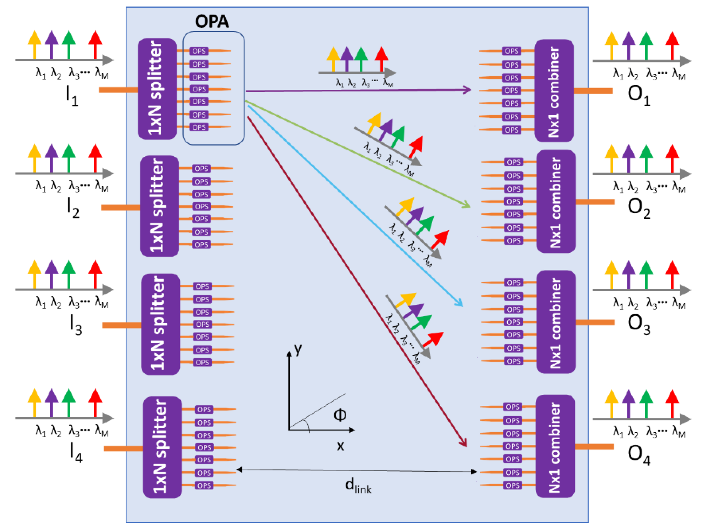
The proposed 4 × 4 OWS configuration, based on the use of OPAs with seven antennas, increases the number of transmitters and receivers that can be connected by the same wireless switch. This adds a further building block for on-chip wireless interconnection networks, thus opening new possibilities for the network design space exploration.
(2)
The design criteria for the OPA are identified and the OWS performances are analyzed and optimized by the Finite Difference Time Domain (FDTD) numerical simulations.
(3)
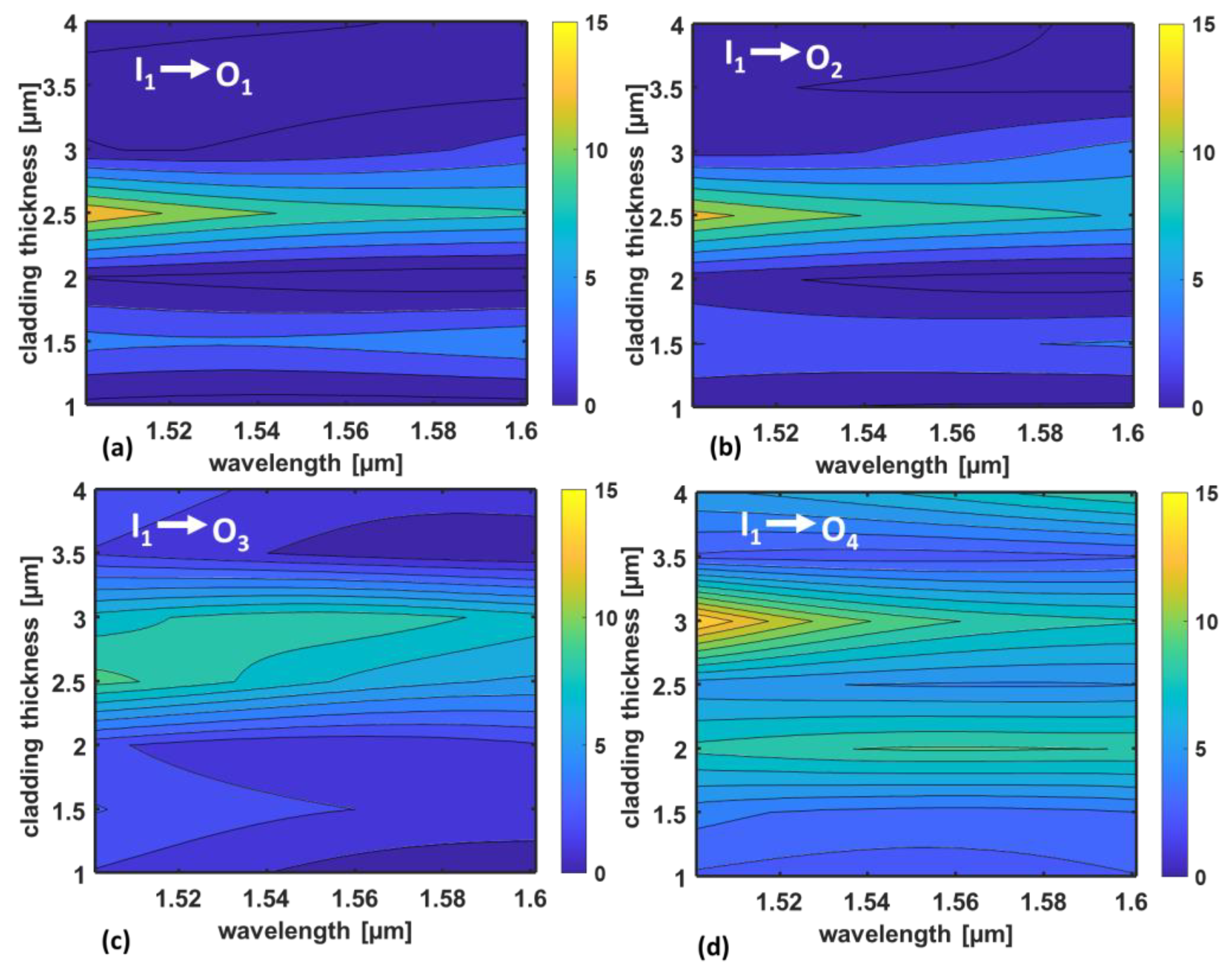
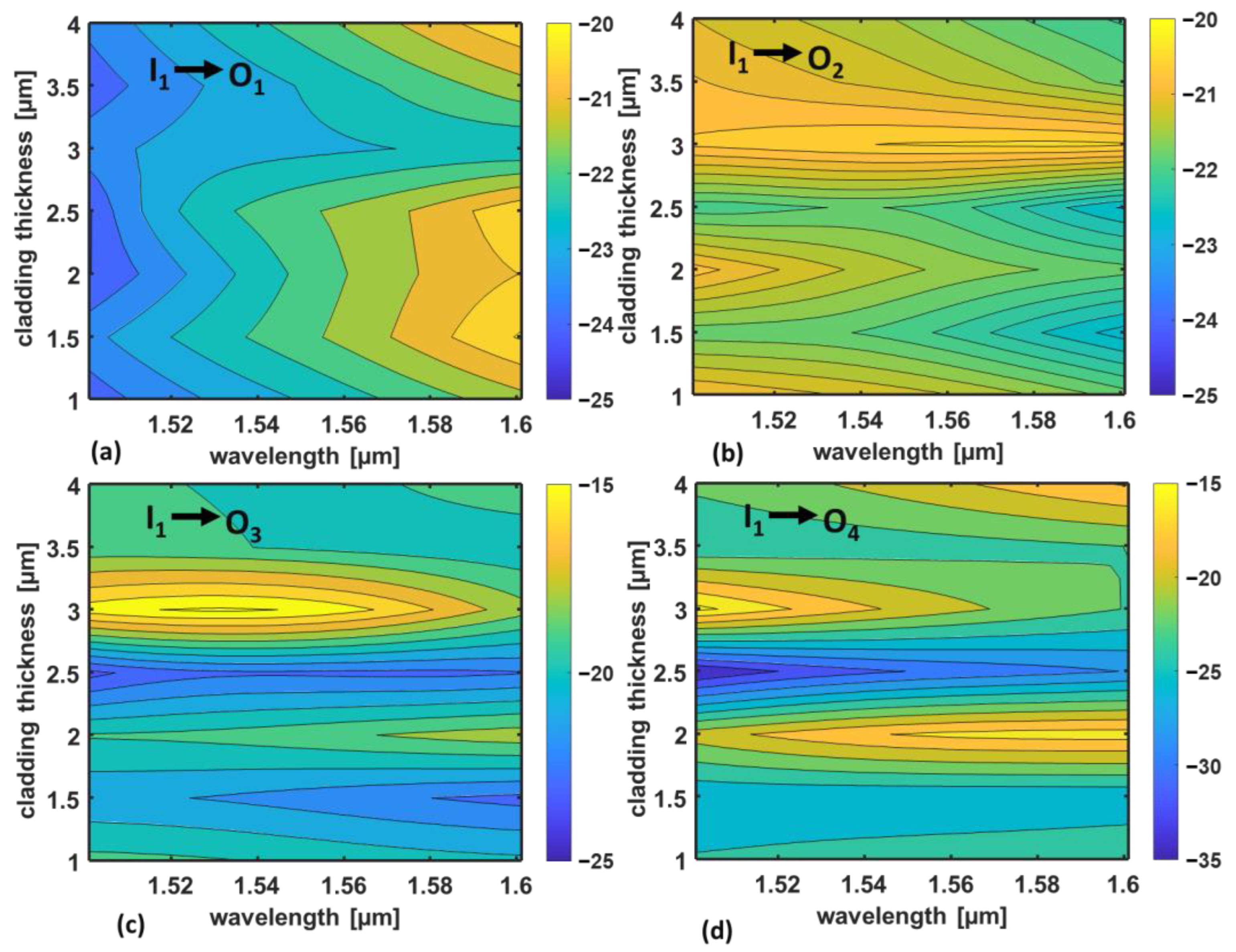
The effect of multipath propagation in the multi-layer on-chip structure is evaluated, showing that the device performances can be optimized, in terms of insertion loss and crosstalk, by varying the cladding layer thickness.
(4)
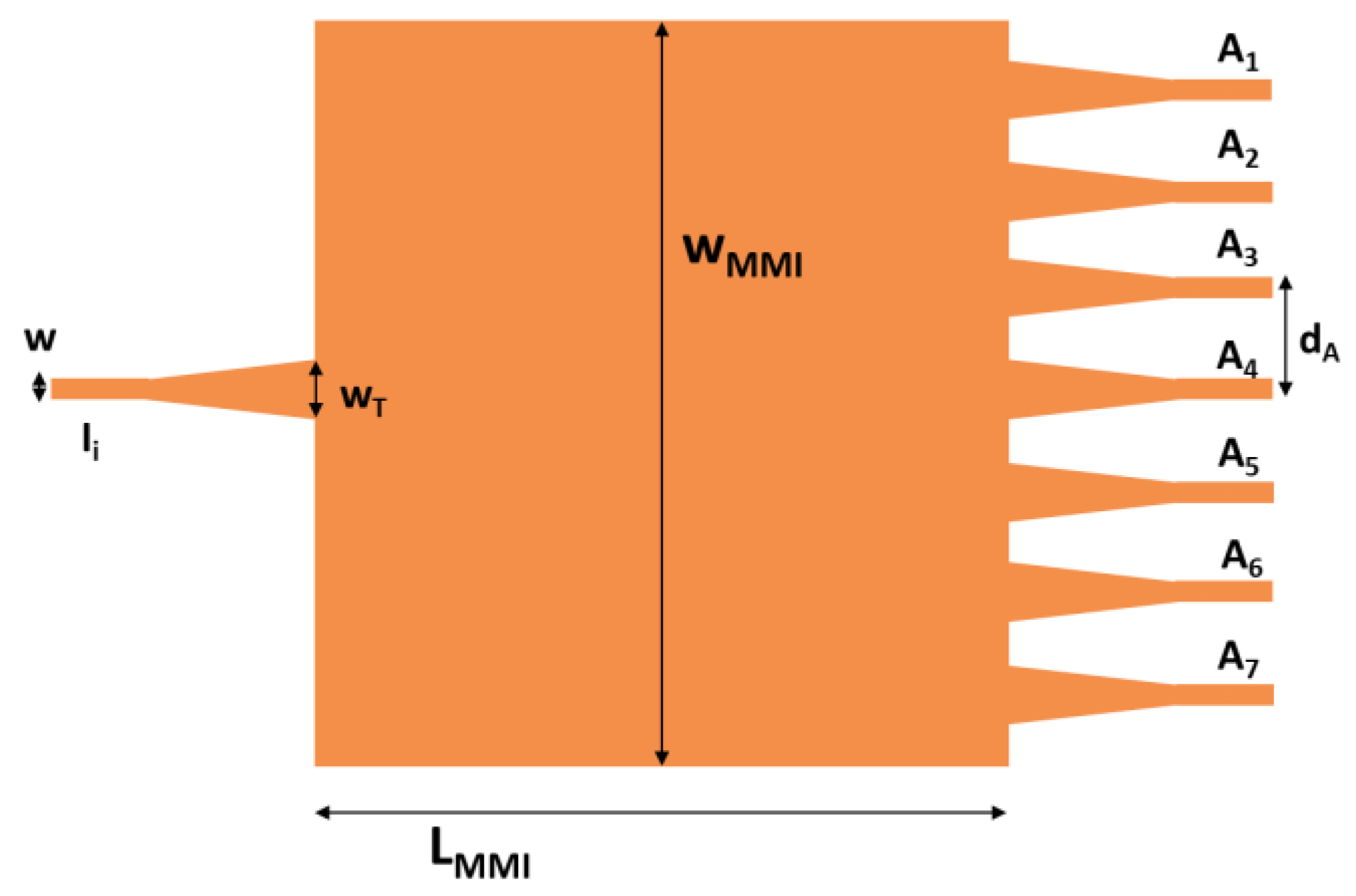
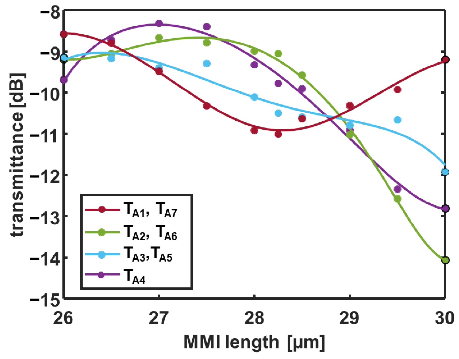
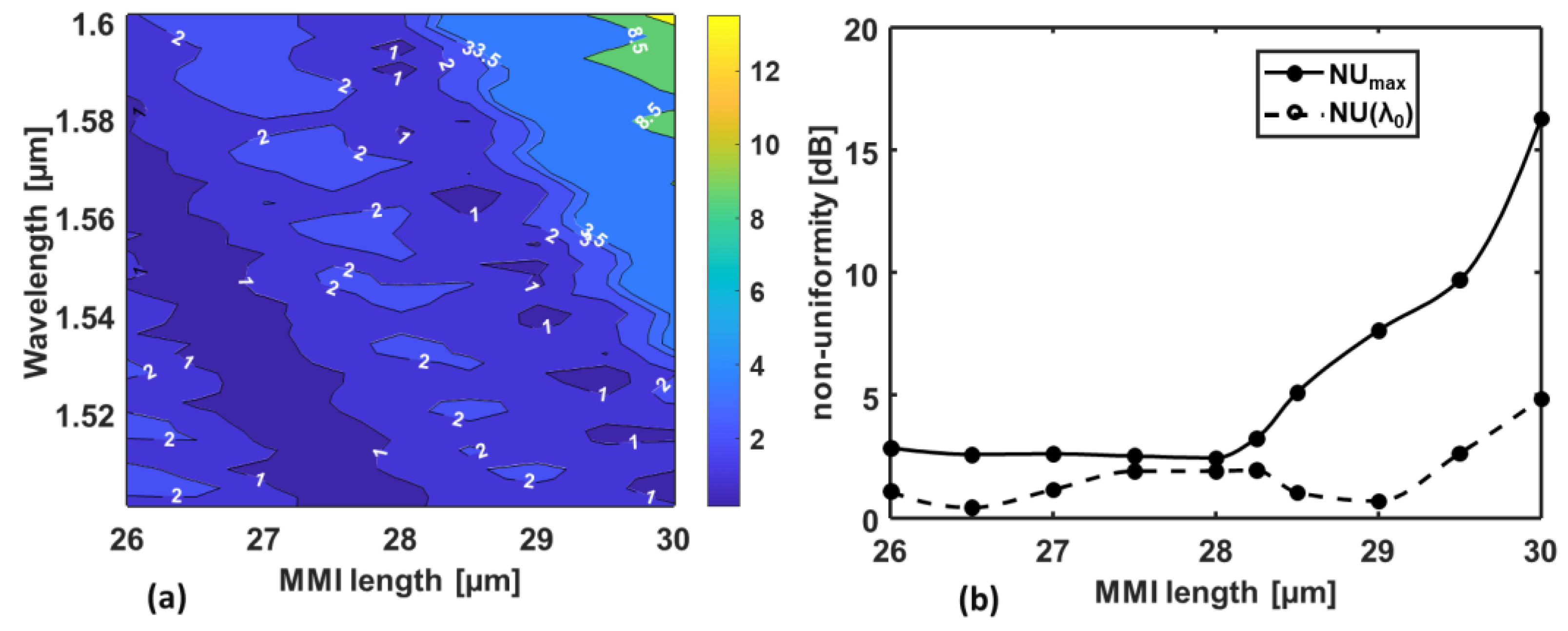
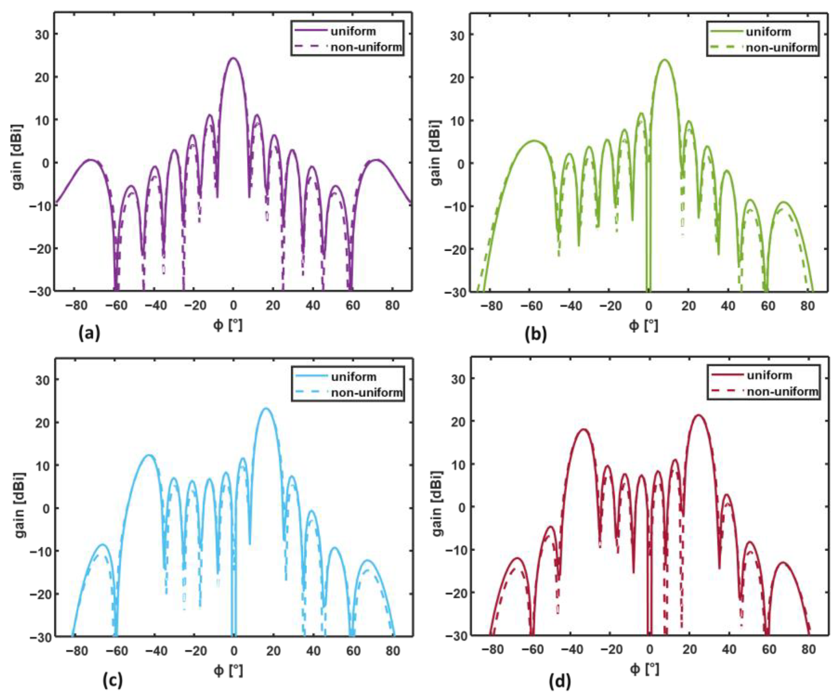
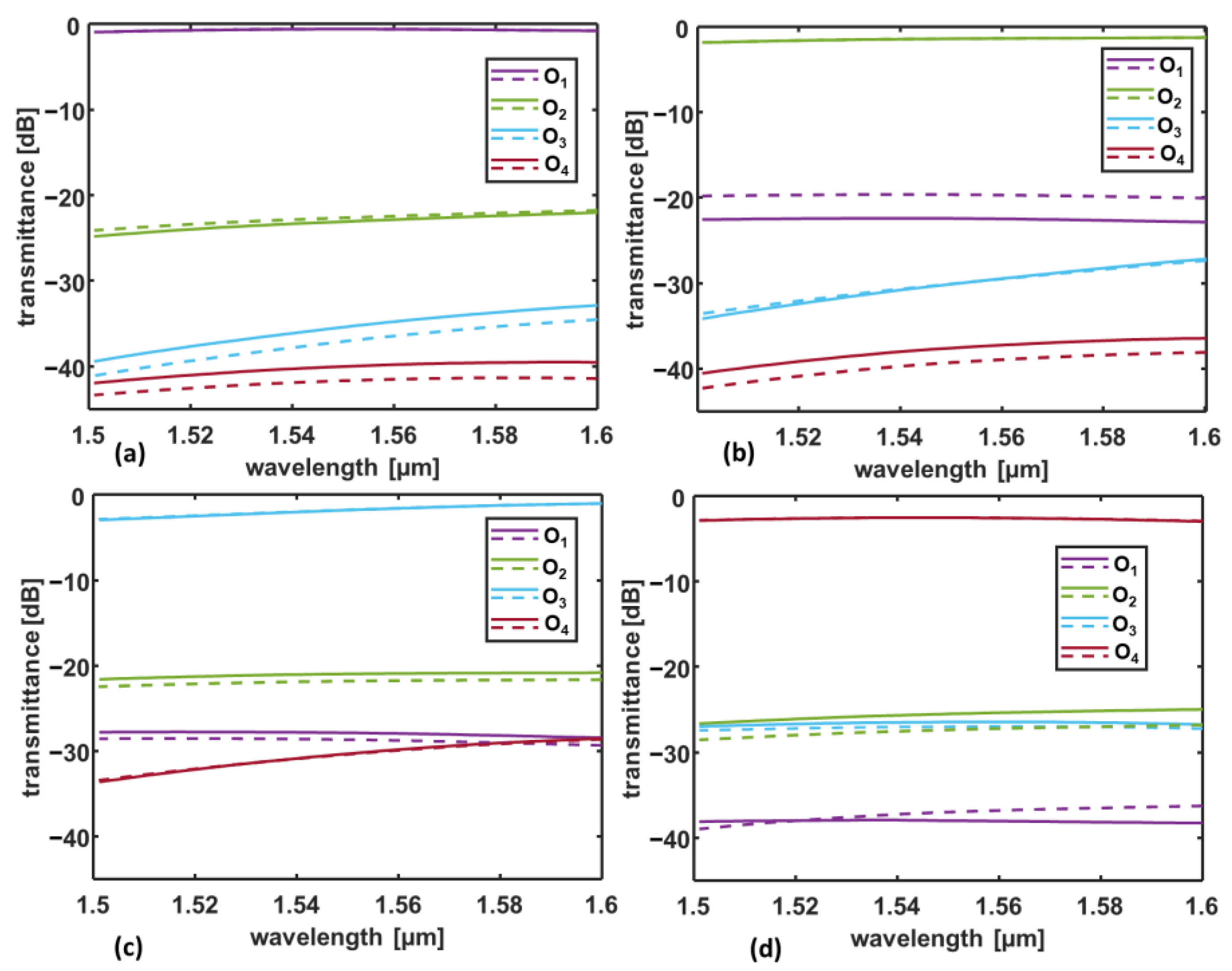
The effect on the OWS behavior of a non-ideal distribution of the power in input to the OPA is investigated. For this purpose, we first report the results of the design of a 1 × 7 beam splitter, based on a Multi-Mode Interference (MMI) device. Then, the MMI output signals are considered in input to the transmitting OPA to evaluate the effect of the non-uniform distribution of the OPA input on the performances of the OWS. This analysis shows that the OWS performances are not significantly affected by a non-ideal distribution of power in input to the OPA.
In Section 2, the OPA radiation characteristics are investigated and the performances of the OWS are analyzed by the Finite Difference Time Domain (FDTD) numerical simulations.
In Section 3, the effect on the OWS behavior of a non-ideal distribution of the power in input to the OPA is investigated. Finally, the discussion of the results and the conclusions are reported in Section 4 and Section 5.

2. 4 × 4 Optical Wireless Switch

The proposed reconfigurable optical wireless switch is schematized in Figure 1. It exploits optical phased arrays made of seven antennas to connect four inputs (i.e., Ii with i = 1, 2, 3, 4) with four outputs (i.e., Oi with i = 1, 2, 3, 4). A wavelength division multiplexing signal, with M channels associated with M different wavelengths, is launched in input to one of the OPAs (e.g., I1), and it is distributed to the seven antennas through a 1 × 7 beam splitter. Each antenna receives, in input, all the WDM channels, radiating them in the surrounding space.
The beam radiated by the OPA, given by the superposition of the electromagnetic field radiated by each antenna, can be steered toward the addressed receiver, as schematized by the colored arrows in Figure 1, thanks to the phase shift α induced by the Optical Phase Shifters (OPSs). To guarantee efficient communication, it is also necessary to virtually steer the radiation diagram of the receiving OPA toward the transmitter. This can be accomplished by applying a corresponding phase shift—α also at the addressed receiver. The received signal is then recombined in the output waveguide by an N × 1 combiner.
The OWS operation principle is similar to that of the 3 × 3 configurations proposed by the authors in [37], but here, seven antennas are used in the OPA to increase the number of inputs and outputs. In fact, by suitably choosing the phase shift α, a 4 × 4 connectivity can be achieved with the seven-antenna OPAs.
In the following subsections, the radiation characteristics of the seven-antenna OPA are first analyzed, and then the full device performances are evaluated.

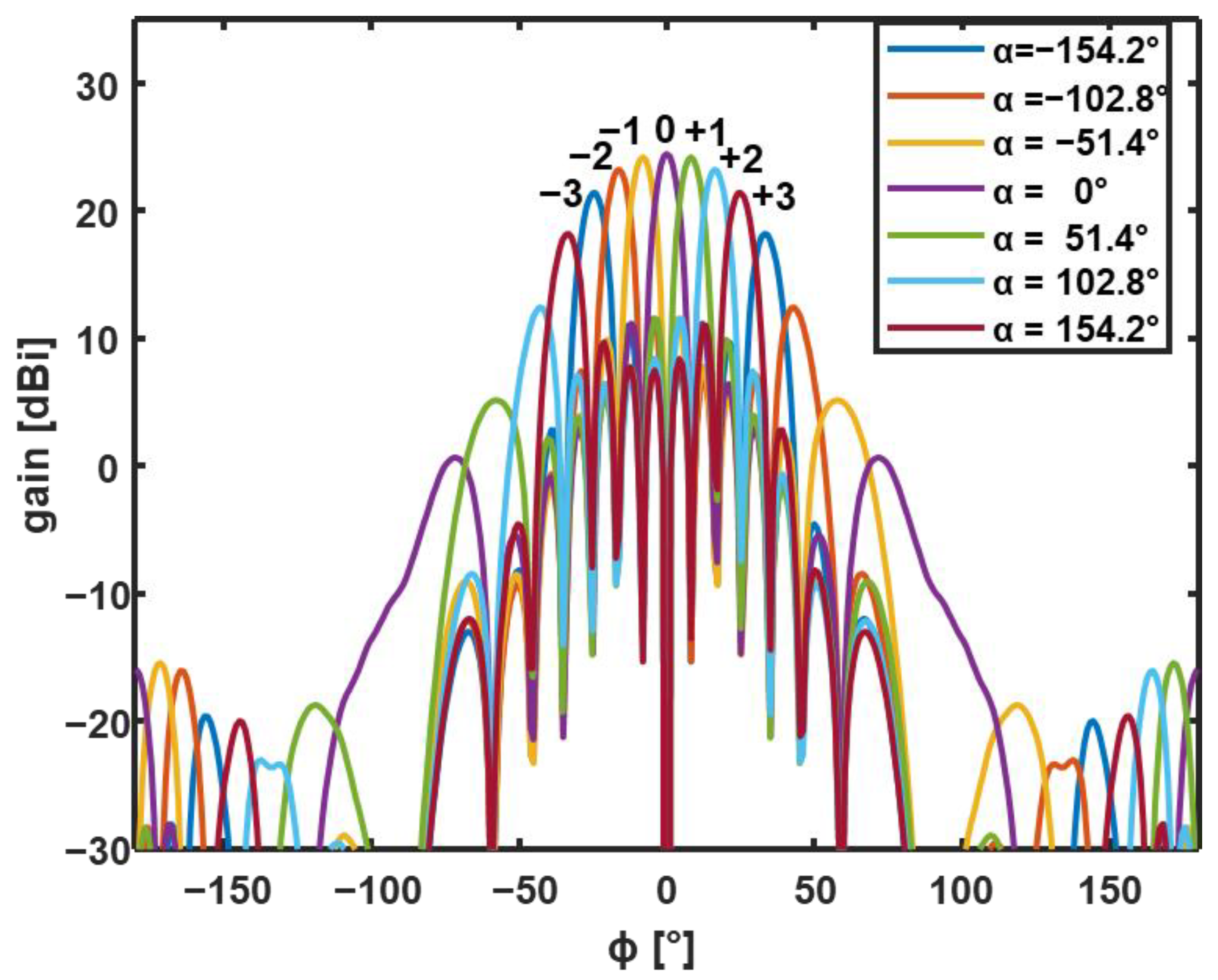
2.1. Optical Phased Array Radiation Diagram

The OPAs at the transmitting and receiving nodes are made by aligning seven taper antennas along the y axis. Each antenna is obtained by inversely tapering a standard SOI waveguide (cross-section height h = 220 nm and width w = 450 nm), terminated on a small tip (length l = 1 μm, and width wT = 130 nm) [34]. The distance between the antennas in the OPA is chosen to be equal to d = λm, where λm is the wavelength in the surrounding medium, where the radiation occurs. According to antenna theory, the distance d = λm guarantees that the OPA exhibits only a main radiation lobe, which can be steered by suitably phase-shifting the antenna input signals [39]. In particular, considering a uniform linear array configuration, the phase shift α between two adjacent antennas is constant.
The characteristics of the taper antenna have already been investigated by the authors in [37,38], through three-dimensional FDTD simulations with standard near-to-far field transformation [40]. This antenna radiates mainly in the direction of the mode propagation (i.e., the x axis in the reference system in Figure 1). Moreover, its gain increases with the taper length LT, with a corresponding decrease in the half-power beam width, i.e., the angular aperture of the radiated beam. Further details on the radiation characteristics of the single-taper antenna can be found in [37,38].
The overall radiation diagram of a uniform linear array made of Na identical antennas can be obtained through the multiplication of the electromagnetic field radiated by the single antenna by the array factor (AF), expressed as [38,39]:
AF = q = 1 N a a q e j ( q 1 ) [ kd sin ( ϕ ) + α ]
where aq is the excitation amplitude of each element, and k = 2π nm/λ is the propagation constant in a homogeneous medium with the refractive index nm at the wavelength λ. The angle ϕ shown in the scheme of Figure 1 is defined considering the spherical coordinate reference system, where r is the modulus of the position vector r that identifies the calculation point, θ is the inclination angle (between r and the z axis), and ϕ is the azimuthal angle (angle of rotation from the x axis). The behavior of a one-dimensional array is well described considering the plane identified by the direction x of maximum radiation for the single antenna and the axis y of the alignment of the array. Therefore, in the following, the radiation characteristics of the OPA are reported considering the xy plane, and they are represented as a function of the angle ϕ.
According to Equation (1), Figure 2 shows the gain of the OPA as a function of the angle ϕ calculated for an array of Na = 7 taper antennas and for different values of the phase shift α. The distance between two adjacent antennas in the OPA is equal to d = λm, whereas the taper length is LT = 2 μm. The gain G(θ, ϕ) is calculated as [39]:
G   ( θ , ϕ ) = 4 π I ( θ , ϕ ) P in
where I(θ, ϕ) is the radiation intensity in spherical coordinates and in the far-field region, and Pin is the total power in the input to the array, given by the sum of the power values in the input to each antenna waveguide.
For each value of the phase shift α, the radiation diagram of the OPA exhibits a main lobe and several side lobes and radiation nulls in the xy plane, i.e., the plane identified by the direction x of maximum radiation for the single antenna and the axis y of alignment of the array. The phase shift values α = ±p360°/Na, with p = 1, 2, 3, are chosen to steer the main beam on the same positions of the nulls of the broadside (α = 0°) array, thus minimizing the crosstalk. In Figure 2, each of the seven main lobes, highlighted by a different number, corresponds to an addressable receiver. As analyzed in [38], the magnitude of the main radiation lobes, for the different values of the phase shift α, follows the envelope of the single-antenna radiation diagram. Therefore, according to the single-antenna radiation characteristics, the taper length LT = 2 µm (i.e., short-taper condition) has been chosen to minimize the variation in the maximum gain of the steered beams and, therefore, the difference in the power received by the different output OPAs.

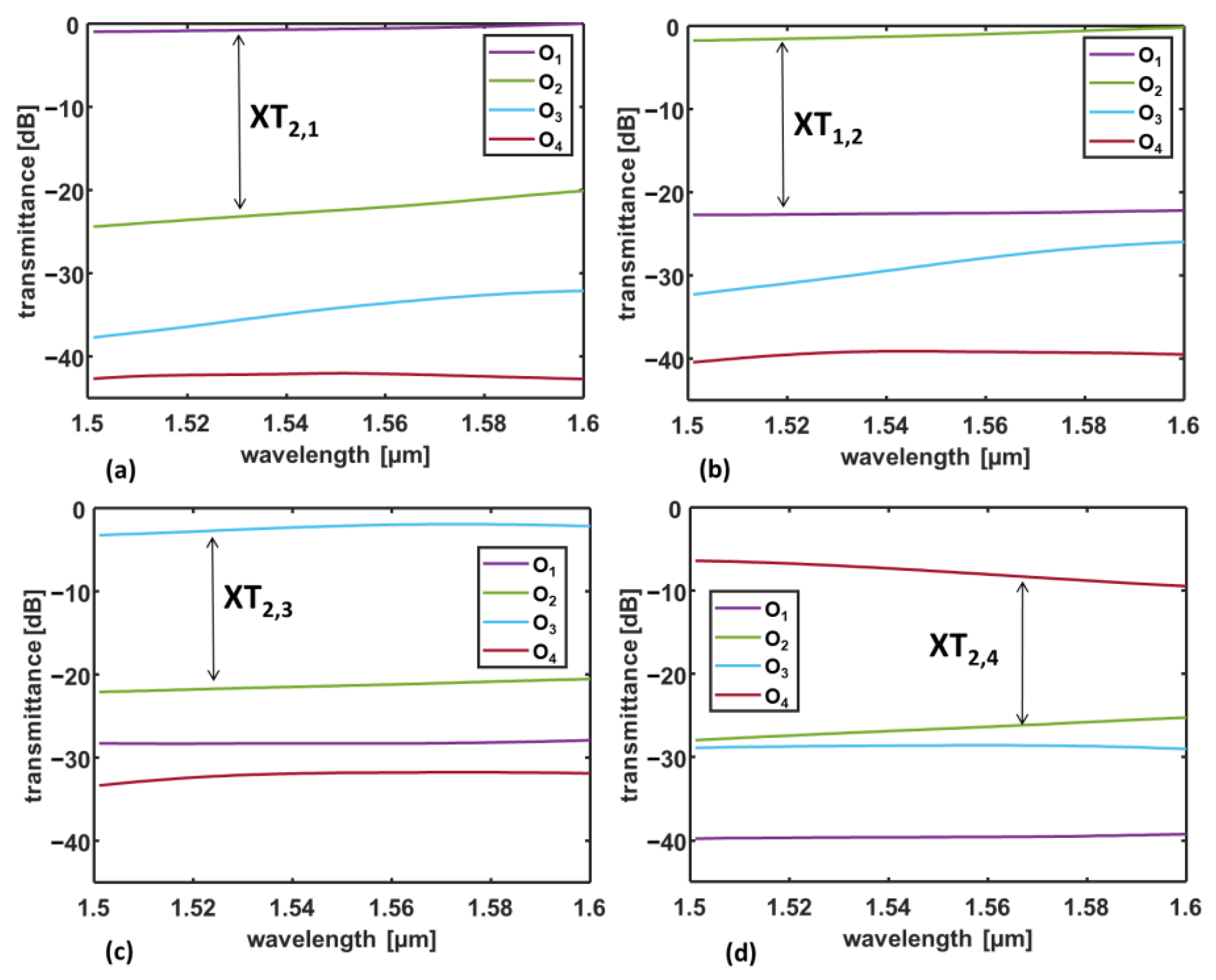
2.2. 4 × 4 OWS Operation Principle and Performances

Considering the radiation diagrams shown in Figure 2, the different connections between the transmitting and the receiving nodes of the 4 × 4 OWS can be explained.
When α = 0°, the main radiation occurs at ϕ = 0°, i.e., in front of the OPA. Therefore, considering the scheme in Figure 1, if I1 is transmitting, the receiver O1 can be illuminated when α = 0°. Similarly, when α = +p360°/Na, with p = 1, 2, 3, the receivers Oi, with i = 2, 3, 4, can be addressed.
The transmitter I2 can be connected to O1 when α = −360°/Na = 51.4°, whereas it can be connected to O2 when α = 0° and to the other receivers O3 and O4 when α is, respectively, α = +360°/Na = 51.4° and α = +2∙360°/Na = 102.8°.
Extending the same concepts to all the transmitters and receivers, the connectivity table (see Table 1) for the 4 × 4 OWS can be derived. Table 1 reports the phase shifts α required for connecting the four Ii transmitters with the four receivers Oi.
A numerical model of the 4 × 4 OWS was implemented by the FDTD method [40] considering the electromagnetic propagation in a multilayer medium, which is representative of the on-chip structure of photonic integrated circuits. In particular, we first considered a multilayer structure corresponding to the sample fabricated and characterized by the authors in [41] for the evaluation of point-to-point wireless links. It consists of a standard Silicon-on-Insulator (SOI) sample, with a bottom layer of bulk silicon Si (with a refractive index nSi = 3.457), an overlying layer of silicon dioxide SiO2 (with a height equal to 3 µm and a refractive index nSiO2 = 1.445), and another layer of Si (220 nm-thick), where the standard waveguides and the antennas are patterned. A further thin layer of borophosphorous tetraethyl orthosilicate (BPTEOS) (of a height equal to 300 nm and a refractive index nBPTEOS = 1.453) was considered on top of the antennas to improve the homogeneity of the refractive index around the antennas. The BPTEOS is then covered with a UV26 polymer cladding layer (with a thickness t = 3.78 µm and a refractive index nUV26 = 1.526). The last layer of the multilayer stack, considered in the simulations, is air. Both the bottom bulk Si layer and the top air layer are considered as semi-infinite by using Perfectly Matched Layer (PML) boundary conditions.
The behavior of the 4 × 4 OWS can be fully described by considering the connection between the transmitter I1 and the four receivers Oi, with i = 1, 2, 3, 4, thanks to the symmetry of the radiation diagrams. Figure 3 shows the transmittances TOi in dB, calculated as a function of the wavelength, at the receiving OPAs, i.e., O1, O2, O3, and O4, when the transmitting OPA I1 is excited with phase shifts: (a) α = 0°, (b) α = 51.4°, (c) α = 102.8°, and (d) α = 154.2°. The link distance dlink = 70 μm was arbitrarily chosen. Figure 3 agree with the connectivity table (Table 1), as the addressed receivers exhibit high transmittance values. Nonetheless, a small part of the signal is also received by the non-addressed outputs, thus originating crosstalk.
To better quantify the OWS performances, we define the insertion loss as:
ILj=−10∙Log10(TOj)
where TOj is the transmittance at the addressed output Oj, and we define the crosstalk as:
XT i , j = 10 Log 10 ( T Oi T Oj )
where TOi is the transmittance of a non-addressed port. The arrows in Figure 3 highlight, for each phase-shift, the curves from which the maximum XTi,j is calculated according to Equation (3).
Considering Figure 3, the worst-case insertion loss and crosstalk occur when the link between the transmitter and the further receiver O4 is considered (Figure 3d). It is worth pointing out that the simulations take into account the propagation in the multilayer structure, which is affected by multiple reflections at the media interfaces. This phenomenon causes constructive or destructive interference that depends on the multilayer characteristics, such as layer thicknesses, refractive indices, and the OPA radiation diagram [41,42].
Therefore, the thickness of the cladding layer is one of the parameters that can be engineered to improve the OWS performances, especially in terms of insertion loss.
In Figure 4 and Figure 5, the results of the parametric analysis of the insertion loss and crosstalk, as a function of the UV26 layer thickness, are reported. In particular, Figure 4 shows the insertion loss ILj in dB, calculated as a function of the wavelength and of the cladding thickness t, at the receiving OPAs, i.e., O1, O2, O3, and O4, when the transmitting OPA I1 is excited: (a) IL1, (b) IL2, (c) IL3, and (d) IL4.
In Figure 4, for fixed values of the wavelength, the variation in the insertion loss with the cladding thickness is mainly due to the different multipath contribution that causes constructive or destructive interference. The worst-case insertion loss occurs around the thickness t = 2.5 µm when the receivers O1, O2, and O3 are considered, whereas it occurs around t = 3 µm for the receiver O4, which, in general, exhibits higher insertion loss values. Considering Figure 4, for many of the values of the thickness t, the variation in ILj with the wavelength is limited to less than 3 dB, thus confirming that a wideband operation of the OWS can be achieved. This is particularly relevant when WDM communication schemes are implemented. Therefore, the layer thickness can be optimized to reduce the insertion loss while ensuring broadband communication. In particular, the configuration that minimizes the insertion loss at the further receiver O4 (i.e., insertion IL4 < 2.8 dB in the whole wavelength range) corresponds to t = 1 µm.
Moreover, Figure 5 reports the maximum crosstalk in dB, calculated as a function of the wavelength and of the cladding thickness, at the receiving OPAs, i.e., O1, O2, O3, and O4, when the transmitting OPA I1 is excited: (a) XT21, (b) XT12, (c) XT23, and (d) XT24. To ease the readability of Figure 5, the color scales have been adapted to the range of variation of the XT values. Considering the XT values shown in Figure 5, the crosstalk remains, in general, below −15 dB. For the thickness t = 1 µm, the worst-case crosstalk XT23 is below −18 dB in the whole wavelength range.
The results reported above consider, in the input to OPA, an ideal 1 × 7 beam splitter that equally divides the input signal into the OPA antennas. In the following, we aim to investigate the effect on the OWS performances of a non-ideal behavior of the 1 × 7 splitter.
The phase shift necessary for the optical wireless switch operation can be achieved in silicon waveguides by using optical phase shifters based either on thermo-optic or plasma-optic effects [43]. Thermally controlled waveguide phase shifters could be preferred because they are based on relatively simple and robust structures, and their fabrication is less prone to errors. Conversely, plasma-optic phase shifters are expected to outperform the thermal effect in terms of switching speed.
For example, reference [44] reports the design and the experimental results of thermo-optic phase-shifters based on TiN metal and N++-doped silicon. The phase shifters proposed in [44] show negligible losses and have very stable power consumption. Considering the results reported in [44], the power Pπ necessary to achieve a π phase shift with thermo-optic phase-shifters based on TiN metal is equal to Pπ = 21.4 mW.
If Pq is the power required for phase shifting each antenna in the array (identified by the index q), the total power for steering the optical phased array with Na = seven antennas is P O P A = q = 1 N a P q .
Indeed, the power Pq depends on the chosen phase shifter technology and on the array requirements. The power required for achieving a generic phase shift γ can be roughly estimated as Pi = Pπ γ/π, given the almost linear dependence of the phase shift on the thermo-optic heater power.
Considering Equation (1), the phase shift applied to the qth antenna is equal to γq = (q − 1)α. If γq is greater than 360°, the angle γq can be converted into the corresponding angle in the [0°, 360°] range by the following equation:
γ q eq = γ q γ q 2 π 2 π  
where q is the index denoting the different antennas in the array and γ q / 2 π is the greatest integer less than or equal to γ q / 2   π (i.e., floor operation).
Considering a thermal phase shifter, as in [44], the power necessary to phase shift each antenna in the array can be calculated as:
P q = P π π γ q eq
In the analyzed optical wireless switch, the phase shift values α = ±p360°/Na, with p = 1, 2, 3, are chosen to steer the main beam on the same positions of the nulls of the broadside (α = 0°) array, thus minimizing the crosstalk. The power necessary to steer the optical phased array of the transmitter I1 toward the receiver O4 is q = 1 N a P q = 128 mW. To guarantee efficient communication between I1 and O4, it is also necessary to virtually steer the radiation diagram of the receiving array toward the transmitter. This can be accomplished by applying a corresponding phase shift −α also at the addressed receiver. Therefore, the connection of one transmitter and one receiver would require approximately Ptot = 2∙POPA = 256 mW. Similar values of the total power are obtained for the connection of the other transmitters and receivers.
The power consumption of the switch should be evaluated considering the aggregated data rate that can be achieved. In fact, the common approach in the network on-chip analysis is to consider the energy-per-bit as a figure of merit, rather than the power. The proposed optical wireless switch is a broadband device, and the power required for signal routing is independent of the number of WDM channels allocated in the bandwidth. For example, considering a WDM signal with a channel spacing Δλ = 0.8 nm, virtually 120 channels can be allocated in the simulated 100 nm bandwidth of the optical wireless switch. If the individual optical channel data rate is 50 Gb/s, the estimated energy per bit is equal to about 42 fJ/b. Optimized phase shifter configurations (e.g., based on plasma-optic effect) or higher data rates could result in lower energy-per-bit consumption.

3. Effect of Non-Uniform Power Distribution at the Transmitting OPA Antennas

An ideal 1 × 7 beam splitter would equally distribute the input power to the seven antennas. However, in actual devices, the power distribution at the 1 × N output of the beam splitter can be non-uniform. A possible implementation of the 1 × N beam splitter that brings the signal to the OPSs, and then to the OPA antennas, can be made by cascading multiple 1 × 2 Y junctions to increase the number of outputs [45,46]. A 1 × 2 Y junction keeps the two outputs in phase while equally dividing the input power into the two waveguides. Another possible implementation can exploit the cascade of multiple Multi-Mode Interference (MMI) devices [47,48]. In the case of 1 × 2 MMIs, the power is equally divided at the two outputs, and the signals are in phase.
Possible errors introduced by the 1 × N splitter by a non-uniform power distribution to the OPA antennas can change the performances of the OWS. Additionally, errors in the phase shift between the antennas can have an effect on the switch performances, but they can be compensated by the optical phase shifters. In Si waveguides, OPSs can be implemented by exploiting either thermo-optic or plasma-optic effects [43,44].
Here, we aim at evaluating the effect on the OWS performances of a non-uniform power distribution to the input OPA antennas. In particular, we define a case study considering a beam splitter based on a 1 × 7 MMI. This device can be a more compact solution for the beam splitting functionality in a single stage. The MMI beam splitter is based on general interference, which can be explained through self-imaging in multi-mode waveguides [49,50]. Thanks to the self-imaging property, the input field profile is reproduced in multiple images in the multimode section of the MMI, at periodic intervals [50]. Therefore, by suitably choosing the length of the MMI, the input signal can be split into multiple output waveguides.
In the following subsections, we report the results of the design of a 1 × 7 MMI, focusing on the analysis of the uniformity of the output power at the seven ports. Moreover, we evaluate the effect of non-uniform distribution of the power in the input to the antennas by simulating the whole OWS.

3.1. 1 × 7 Multi-Mode Interference Beam Splitter

The proposed 1 × 7 MMI configuration is schematized in Figure 6. The waveguides are made of silicon. Moreover, the same multilayer of the OWS is considered in the simulations, with the UV26 cladding thickness t = 1 µm. The MMI device is, indeed, patterned in the antenna layer, and the input and output waveguides are standard SOI waveguides (cross-section height h = 220 nm and width w = 450 nm). Input and output tapers are considered to improve the output power uniformity, as discussed in [49], with the taper width wT = 1 µm. The distance between the output waveguides was arbitrarily chosen to be equal to dA = 1.50 µm, but in the design of an overall integrated circuit, it can be customized to meet the topological constraints, e.g., for fabrication. The width of the MMI region is chosen to be equal to wMMI = 7∙dA. The optimal length of the MMI can be estimated by the following equation [50]:
L MMI = L π 3 4 N A = λ 0 2 ( n 1 n 2 ) 3 4 N A
where Lπ is defined as the beat length of the two lowest-order modes of the multimode region, NA is the number of outputs, and λ0 is the design wavelength (i.e., 1.55 µm), whereas n1 and n2 are the effective refractive indices of the two lowest-order modes of the MMI.
The length of the MMI, LMMI = 28.6 µm, estimated by Equation (6), must be optimized by the simulation of the full device, taking into account the non-uniformity of the power at the seven outputs. The output power non-uniformity NU, which is a function of the wavelength, can be quantified as:
NU ( λ ) = max i ( T Ai ( λ ) ) min i ( T Ai ( λ ) )
where TAi with i = 1, 2,…7 are the transmittances in dB calculated at the seven output ports of the MMI. Indeed, the non-uniformity is zero when the output transmittances TAi are all equal, and it is greater than zero when the power distribution is non-uniform.
The parametric analysis, as a function of the MMI length LMMI, was performed by three-dimensional FDTD simulations. Figure 7 shows the transmittances TAi calculated at the output ports (in dB) as a function of the MMI length and at the wavelength λ0 = 1.55 µm. Given the symmetry of the device with respect to the central output A4, only four curves are visible in Figure 7. Considering Figure 7, the MMI length that gives the lowest variation of the transmittances (i.e., calculated non-uniformity NU(λ0) = 0.44 dB at the design wavelength λ0 = 1.55 µm) is equal to LMMI = 26.5 µm.
It is worth pointing out that the wavelength behavior of the 1 × N beam splitter can affect the bandwidth of the overall OWS; therefore, it is necessary to analyze the non-uniformity also as a function of the wavelength.
Figure 8a shows the non-uniformity NU calculated in dB as a function of the MMI length and of the wavelength. Moreover, Figure 8b shows the non-uniformity NU(λ0) calculated at the design wavelength λ0 = 1.55 µm (dashed curve) and the maximum non-uniformity in the bandwidth (solid curve) calculated, for each value of LMMI, as:
NU max = max λ ( NU ( λ ) )
As Figure 8 shows, longer values of the MMI length LMMI give higher non-uniformity. Considering Figure 8b, the length value that gives the lowest non-uniformity in the whole analyzed wavelength range, i.e., NU(λ) < NUmax with NUmax = 2.46 dB, is LMMI = 28 µm. The corresponding non-uniformity at the design wavelength is NU(λ0) = 1.93 dB.
The 1 × 7 MMI divider also contributes to the overall insertion loss of the OWS. For the MMI length LMMI = 28 µm, the overall insertion loss of the 1 × 7 MMI, calculated by summing up the power coupled at the seven output waveguides, is about ILMMI = 1.27 dB. Moreover, the calculated back reflection at the input port of the 1 × 7 MMI is below −14 dB in the whole frequency range.
Considering the scheme in Figure 1, each transmitter Ii is equipped with an OPA that radiates the whole signal spectrum (i.e., all the WDM channels) toward the same addressed receiver. At the addressed receiver, all the seven antennas of the OPA contribute to the received power. If the proper phase relation is ensured, as assumed in this paper, the signals received by each antenna in the receiving OPA constructively sum up in the output waveguide. Therefore, the Nx1 combiner is intended to constructively add the signals received by the seven antennas in the receiving OPA and to deliver the resulting signal at the output waveguide.
The worst-case insertion loss from the transmitting to the receiving OPA is about 2.8 dB, which accounts for the wireless connection between the transmitting OPA and the receiving one. Considering the scheme in Figure 1, other elements can contribute to the OWS insertion loss, such as the 1 × 7 beam splitter and the 7 × 1 combiner. Additional loss contributions can be introduced by the propagation loss in silicon waveguides (approximately 0.1 dB/cm [21]) and by the optical phase shifters. For example, the thermo-optic phase shifters proposed in [48] exhibit negligible losses (ILOPS < 0.01 dB).
As discussed in [49], further improvement of the 1 × 7 MMI performance can be achieved by optimizing the taper width. However, the full optimization of the MMI goes beyond the scope of this paper, which mainly intends to focus on the analysis of the effect on the OWS performance of a non-uniform power distribution at the input OPA. Therefore, the studied MMI configurations, whose output signals are assumed in the input to the transmitting OPA, give a reference to quantify the possible non-uniformity of the OPA inputs. It is also worth pointing out that the output signals of the MMI are not in the phase, but their phase difference can be compensated by the OPSs.

3.2. OWS Performance with Non-Uniform Input Power

In order to study the effect on the OWS behavior of a non-uniform power distribution at the input OPA, we decided to consider the case study of the 1 × 7 MMI beam splitter. As discussed above, this device can be preferred to the cascade of multiple 1 × 2 splitters because it is more compact. As a drawback, the output power distribution can be non-uniform, in the sense that the power is not equally divided in the seven outputs. Based on the 1 × 7 MMI analysis, we first consider the modification of the OPA radiation diagram, calculated through antenna theory [39]. Then, the results of the FDTD simulations of the whole OWS are discussed.
Based on the MMI analysis reported above, we define a case study considering the amplitudes at the MMI outputs when LMMI = 28 µm. As mentioned above, this configuration exhibits a non-uniformity NU(λ0) = 1.93 dB at the design wavelength and NU(λ) < 2.46 dB in the whole wavelength range.
Considering the calculation of the OPA radiation diagrams, the variation in the input amplitudes can be taken into account by changing the aq coefficients in the theoretical formula of Equation (1). The array factor AF is then multiplied by the far-field of the single-taper antenna, calculated by FDTD simulation.
In the analyzed case, the seven aq coefficients have been chosen to be equal to the amplitudes of the MMI output signals, calculated at the wavelength λ0 = 1.55 µm. Figure 9 shows the gain as a function of the angle ϕ for an array of Na = seven taper antennas calculated for the uniform (solid curve) and the non-uniform (dashed curves) input amplitude distributions. The four values of the phase shift α necessary for the description of 4 × 4 OWS operation are considered: (a) α = 0°, (b) α = 51.4°, (c) α = 102.8°, and (d) α = 154.2°. In Figure 9 the represented ϕ range was restricted between −90° and 90° to ease the readability of the curves.
As can be seen in Figure 9, the non-uniform amplitude at the OPA antennas slightly changes the level of the side lobes, but it does not significantly change the main lobe level. The main lobe is mainly responsible for the communication between the transmitter and the addressed receiver. Therefore, since it is unaltered, no significant change in the OWS insertion loss is expected for all the phase shift values. Conversely, a change in the crosstalk is expected since it is mainly associated with the sidelobes.
In order to analyze the OWS behavior, the full device has been simulated by the FDTD method. In the FDTD model of the OWS, the transmitting OPA was fed by seven mode sources, each injecting a TE-guided mode into the OPA antennas [40]. The amplitudes of the modes were set equal to the MMI output amplitudes, calculated at the wavelength λ0 = 1.55 µm, thus taking into account the non-uniform power distribution at the 1 × 7 MMI outputs. We have chosen to apply a straightforward simulation approach in which the amplitudes of the seven mode sources do not change with the wavelength.
Figure 10 shows the transmittances in dB, calculated as a function of the wavelength, at the receiving OPAs, i.e., O1, O2, O3, and O4, when the transmitting OPA I1 is excited with uniform (solid curves) and non-uniform (dashed curves) input signals. The phase shift values considered in Figure 10 are: (a) α = 0°, (b) α = 51.4°, (c) α = 102.8°, and (d) α = 154.2°.
Figure 10 shows that the transmittances at the addressed ports do not significantly change when a non-uniform excitation is considered, as expected by the analysis of the radiation diagrams in Figure 9. Conversely, the change in the transmittances at the non-addressed outputs is more pronounced. In particular, a 2.8 dB worsening of the crosstalk XT12 is found for the connection between the transmitter I1 and the receiver O2 (Figure 10b), which now corresponds to the worst-case crosstalk. Nonetheless, the crosstalk XT12 is still below −18 dB in the whole wavelength range.

4. Discussion

The proposed 4 × 4 OWS increases the number of transmitters and receivers that can be connected by the same wireless switch with respect to the configurations previously proposed in [37,38]. This configuration widens the available building blocks for the implementation of optical wireless networks on-chip.
The numerical analysis of the OWS has shown that the worst-case insertion loss is IL = 2.8 dB for the wireless interconnection. The evaluated worst-case crosstalk is −18 dB, and the bandwidth is about 100 nm. The reported results have shown that, thanks to the multipath propagation, the insertion losses can be minimized by suitably choosing the cladding layer thickness for the same switch configuration.
Other state-of-the-art broadband solutions for photonic switching consist of arranging 2 × 2 Mach–Zehnder interferometers into higher-order switching topologies. Owing to their operating principles, Mach–Zehnder interferometers are able to switch multiple wavelengths simultaneously [24,51]. 2 × 2 Mach-Zehnder switches are typically organized into larger N × N switching topologies through carefully optimized connectivity patterns such as Benes or dilated-Benes networks [30,52]. Even though a direct comparison of performances is not straightforward, the crosstalk and insertion losses of the proposed 4 × 4 OWS are comparable with those reported in [30,52]. As a drawback, the power consumption is higher, but it is partly compensated by the broadband behavior, which leads to an acceptable energy-per-bit requirement of about 42 fJ/b.
As future directions of the research, the performances of the 4 × 4 OWS can be further improved by considering optimized phase shifter configurations, e.g., based on the plasma-optic effect, which can reduce the power requirement. Moreover, the OWS insertion losses can be further improved by optimizing the design of the beam splitters and combiners and by considering different single antennas in the OPAs.
In the proposed configuration, the OPAs exploit seven dielectric taper antennas. Nonetheless, the proposed design criteria can be applied to virtually any kind of integrated antennas. Other possible implementations of integrated dielectric antennas have been proposed in [34,53], reaching high gain values for the single-antenna radiation (e.g., greater than 20 dBi). The use of high-gain single radiators can increase the overall gain of the OPA, thus contributing to the insertion loss reduction. As a drawback, these antennas have sizes in the order of 15 µm or 25 µm, thus increasing the device footprint. Other, more compact antenna configurations can be implemented through integrated plasmonic antennas. Different configurations of plasmonic antennas have been proposed in the literature for on-chip wireless communications [54,55,56,57]. The plasmonic antennas have very small dimensions (a few microns), but they suffer non-negligible losses due to plasmonic mode propagation in the lossy metal. These losses limit the maximum achievable antenna gain, which is, in general, in the order of 10 dBi or 15 dBi. A wide range of possibilities are therefore available for studying new OWS configurations based on the identified design criteria.
The proposed OWS technology, capable of implementing broadband, low-latency communication among multiple transmitters and receivers, can find application in both long-haul optical communications and short-reach optical interconnects [58,59]. Integrated optical multi-port switches, ensuring reconfigurability and high bandwidth, can find application, for example, in photonic internet network nodes or in the interconnection of multiple chiplets in 2.5D manycore systems. Further future innovative applications can be investigated in quantum communication networks to reduce latency and increase the overall bitrate [60,61,62,63].

5. Conclusions

A 4 × 4 OWS based on reconfigurable OPAs has been proposed for on-chip wireless interconnection. Each OPA exploits seven taper antennas to radiate an optical beam toward the addressed receiving OPA, thanks to the beam steering capability.
The OWS performances have been analyzed and optimized considering the electromagnetic propagation in on-chip multilayer structures, with different thicknesses of the cladding UV26 layer. The optimized configuration exhibits worst-case insertion loss and crosstalk below 2.8 dB and −18 dB, respectively, in the whole wavelength range. The broadband operation of the OWS, which covers the entire C-band, can allow for the implementation of WDM communication schemes. Moreover, all the allocated WDM channels can be switched at the same time, thus making the power requirement for signal routing independent of the number of WDM channels.
As a further step of the analysis, the effect on the OWS behavior of a non-ideal distribution of the power in the input to the OPA has been investigated. For this purpose, a 1 × 7 beam splitter, based on a single-stage MMI device, has been designed. Then, the MMI output signals were considered in the input to the transmitting OPA. The designed 1 × 7 MMI is characterized by a non-uniformity of the output signals below 2.46 in the whole wavelength range. Considering this non-uniform signal distribution at the antennas of the input OPA, the performances of the OWS do not change significantly, showing a good robustness to input amplitude errors.

Author Contributions

Conceptualization: G.C., G.B., F.F., M.B., D.B., V.T. and V.P. Methodology: G.C., G.B., F.F., M.B., D.B., V.T. and V.P. Software: G.C. and G.B. Validation: G.C. and G.B. Investigation: G.C., G.B., F.F., M.B., D.B., V.T. and V.P. Data curation: G.C., G.B., F.F., M.B., D.B., V.T. and V.P. Writing—original draft preparation: G.C., G.B., F.F., M.B., D.B., V.T. and V.P. Writing—review and editing: G.C., G.B., F.F., M.B., D.B., V.T. and V.P. Supervision: G.C. All authors have read and agreed to the published version of the manuscript.

Funding

This work was partly supported by the “IMPACT” project, funded by Apulia region under the call “Progetti di ricerca scientifica innovativi di elevato standard internazionale (art. 22 della legge regionale 30 Novembre 2019, n. 52)”, by the project “Integrated Magneto-Biplasmonic Circulator For Silicon Platform (IMPACTS)”, funded under the call Galileo 2022/Galilée 2022, and by the European Union under the Italian National Recovery and Resilience Plan (NRRP) of NextGenerationEU, partnership on “Telecommunications of the Future” (PE00000001-program “RESTART”).

Institutional Review Board Statement

Not applicable.

Informed Consent Statement

Not applicable.

Data Availability Statement

The data that support the findings of this study are available from the corresponding author upon reasonable request.

Conflicts of Interest

The authors declare no conflict of interest.

References

  1. Flich, J.; Bertozzi, D. (Eds.) Designing Network-on-Chip Architectures in the Nanoscale Era; CRC Press: Boca Raton, FL, USA, 2019. [Google Scholar]
  2. Nychis, G.; Fallin, C.; Moscibroda, T.; Mutlu, O.; Sesharr, S. On-chip networks from a networking perspective: Congestion and scalability in many-core interconnects. Comput. Commun. Rev. 2012, 42, 407–418. [Google Scholar] [CrossRef]
  3. Zia, M.; Wan, C.; Zhang, Y.; Bakir, M. Electrical and photonic off-chip interconnection and system integration. In Optical Interconnects for Data Centers; Woodhead Publishing: Cambridge, UK, 2017; pp. 265–286. [Google Scholar]
  4. Shacham, A.; Bergman, K.; Carloni, L.P. On the design of a photonic network-on-chip. In Proceedings of the 1st International Symposium on Networks-on-Chip (NOCS’07), Princeton, NJ, USA, 7–9 May 2007; pp. 53–64. [Google Scholar]
  5. Terzenidis, N.; Moralis-Pegios, M.; Pitris, S.; Mourgias-Alexandris, G.; Mitsolidou, C.; Fotiadis, K.; Vyrsokinos, K.; Alexoudi, T.; Pleros, N. Board- and rack-scale optical interconnection architectures for disaggregated data centers. In Proceedings of the SPIE, Optical Interconnects XX, San Francisco, CA, USA, 4–6 February 2020; p. 1128606. [Google Scholar]
  6. Deb, S.; Mondal, H.K. Wireless network-on-chip: A new era in multi-core chip design. In Proceedings of the 25th IEEE International Symposium on Rapid System Prototyping, New Delhi, India, 16–17 October 2014; pp. 59–64. [Google Scholar]
  7. Lemic, F.; Abadal, S.; Tavernier, W.; Stroobant, P.; Colle, D.; Alarcon, E.; Marquez-Barja, J.; Famaey, J. Survey on Terahertz Nanocommunication and Networking: A Top-Down Perspective. IEEE J. Sel. Areas Commun. 2021, 39, 1506–1543. [Google Scholar] [CrossRef]
  8. Imani, F.; Abadal, S.; del Hougne, P. Metasurface-Programmable Wireless Network-On-Chip. Adv. Sci. 2022, 9, 2201458. [Google Scholar] [CrossRef] [PubMed]
  9. Abadal, S.; Mestres, A.; Torrellas, J.; Alarcon, E.; Cabellos-Aparicio, A. Medium Access Control in Wireless Network-on-Chip: A Context Analysis. IEEE Commun. Mag. 2018, 56, 172–178. [Google Scholar] [CrossRef]
  10. Gaha, H.I.; Balti, M. Novel bi-UWB on-chip antenna for wireless NoC. Micromachines 2022, 13, 231. [Google Scholar] [CrossRef]
  11. Abadal, S.; Hosseininejad, S.E.; Cabellos-Aparicio, A.; Alarcón, E. Graphene-Based terahertz antennas for area-constrained applications. In Proceedings of the 40th International Conference on Telecommunications and Signal Processing (TSP), Barcelona, Spain, 5–7 July 2017; pp. 817–820. [Google Scholar]
  12. Zhou, J.; Wang, J.; Zhu, L.; Zhang, Q. Silicon Photonics for 100Gbaud. J. Light. Technol. 2021, 39, 857–867. [Google Scholar] [CrossRef]
  13. Liu, A.; Liao, L.; Rubin, D.; Nguyen, H.; Ciftcioglu, B.; Chetrit, Y.; Izhaky, N.; Paniccia, M. High-speed optical modulation based on carrier depletion in a silicon waveguide. Opt. Exp. 2007, 15, 660–668. [Google Scholar] [CrossRef]
  14. Thomson, D.J.; Gardes, F.Y.; Hu, Y.; Mashanovich, G.; Fournier, M.; Grosse, P.; Fedeli, J.-M.; Reed, G.T. High contrast 40 Gbit/s optical modulation in silicon. Opt. Exp. 2011, 19, 11507–11516. [Google Scholar] [CrossRef]
  15. Calò, G.; Alexandropoulos, D.; Petruzzelli, V. Active WDM filter on dilute nitride quantum well photonic band gap waveguide. Prog. Electromagn. Res. Lett. 2012, 35, 37–49. [Google Scholar] [CrossRef]
  16. Calò, G.; Farinola, A.; Petruzzelli, V. Equalization in photonic bandgap multiwavelength filters by the Newton binomial distribution. J. Opt. Soc. Am. B Opt. Phys. 2011, 28, 1668–1679. [Google Scholar] [CrossRef]
  17. Yi, Q.; Zheng, S.; Yan, Z.; Cheng, G.; Xu, F.; Li, Q.; Shen, L. Silicon photonic flat-top WDM (de)multiplexer based on cascaded Mach-Zehnder interferometers for the 2 µm wavelength band. Opt. Express 2022, 30, 28232–28241. [Google Scholar] [CrossRef] [PubMed]
  18. Abadian, S.; Magno, G.; Yam, V.; Dagens, B. Broad-band plasmonic isolator compatible with low-gyrotropy magneto-optical material. Opt. Express 2021, 29, 4091–4104. [Google Scholar] [CrossRef]
  19. Calò, G.; Mescia, L.; Petruzzelli, V.; Prudenzano, F. Study of gain in photonic bandgap active InP waveguides. J. Opt. Soc. Am. B. Opt. Phys. 2009, 26, 2414–2422. [Google Scholar] [CrossRef]
  20. Mirza, A.; Sunny, F.; Walsh, P.; Hassan, K.; Pasricha, S.; Nikdast, M. Silicon Photonic Microring Resonators: A Comprehensive Design-Space Exploration and Optimization Under Fabrication-Process Variations. IEEE Trans. Comput. Aided Des. Integr. Circuits Syst. 2022, 41, 3359–3372. [Google Scholar] [CrossRef]
  21. Thonnart, Y.; Bernabe, S.; Charbonnier, J.; Bernard, C.; Coriat, D.; Fuguet, C.; Tissier, P.; Charbonnier, B.; Malhouitre, S.; Saint-Patrice, D.; et al. POPSTAR: A Robust Modular Optical NoC Architecture for Chiplet-based 3D Integrated Systems. In Proceedings of the 2020 Design, Automation and Test in Europe Conference and Exhibition (DATE), Grenoble, France, 9–13 March 2020; pp. 1456–1461. [Google Scholar]
  22. Calò, G.; D’Orazio, A.; Grande, M.; Marrocco, V.; Petruzzelli, V. Active InGaAsP/InP photonic bandgap waveguides for wavelength-selective switching. IEEE J. Quantum Electron. 2011, 47, 172–181. [Google Scholar] [CrossRef]
  23. Calò, G.; Alexandropoulos, D.; Petruzzelli, V. Active photonic band-gap switch based on GalnNAs multiquantum well. IEEE Photonics J. 2012, 4, 1936–1946. [Google Scholar] [CrossRef]
  24. Lu, L.; Zhao, S.; Zhou, L.; Li, D.; Li, Z.; Wang, M.; Li, X.; Chen, J. 16 × 16 non-blocking silicon optical switch based on electro-optic Mach-Zehnder interferometers. Opt. Express 2016, 24, 9295–9307. [Google Scholar] [CrossRef]
  25. Thirumaran, S.; Dhanabalan, S.S.; Sannasi, I.G. Design and analysis of photonic crystal ring resonator based 6 × 6 wavelength router for photonic integrated circuits. IET Optoelectron. 2021, 15, 40–47. [Google Scholar] [CrossRef]
  26. Calò, G.; Alexandropoulos, D.; D’Orazio, A.; Petruzzelli, V. Wavelength selective switching in dilute nitrides multi quantum well photonic band gap waveguides. Phys. Status Solidi B Basic. Res. 2011, 248, 1212–1215. [Google Scholar] [CrossRef]
  27. Kazmierczak, A.; Bogaerts, W.; Drouard, E.; Dortu, F.; Rojo-Romeo, P.; Gaffiot, F.; Van Thourhout, D.; Giannone, D. Highly integrated optical 4 × 4 crossbar in silicon-on-insulator technology. J. Lightw. Technol. 2009, 27, 3317–3323. [Google Scholar] [CrossRef]
  28. Sherwood-Droz, N.; Sherwood-Droz, N.; Wang, H.; Chen, L.; Lee, B.G.; Biberman, A.; Bergman, K.; Lipson, M. Optical 4 × 4 hitless silicon router for optical Networks-on-Chip (NoC). Opt. Express 2008, 16, 15915–15922. [Google Scholar] [CrossRef] [PubMed]
  29. Cheng, Q.; Bahadori, M.; Hung, Y.H.; Huang, Y.; Abrams, N.; Bergman, K. Scalable microring-based silicon Clos switch fabric with switch-and-select stages. IEEE J. Sel. Top. Quantum Electron. 2019, 25, 3600111. [Google Scholar] [CrossRef]
  30. Lu, L.; Zhou, L.; Li, Z.; Li, X.; Chen, J. Broadband 4 × 4 Nonblocking Silicon Electrooptic Switches Based on Mach–Zehnder Interferometers. IEEE Photonics J. 2015, 7, 7800108. [Google Scholar] [CrossRef]
  31. Alù, A.; Engheta, N. Wireless at the nanoscale: Optical interconnects using matched nanoantennas. Phys. Rev. Lett. 2010, 104, 213902. [Google Scholar] [CrossRef]
  32. Yang, Y.; Li, Q.; Qiu, M. Broadband nanophotonic wireless links and networks using on-chip integrated plasmonic antennas. Sci. Rep. 2016, 6, 19490. [Google Scholar] [CrossRef]
  33. Merlo, J.M.; Nesbitt, N.T.; Calm, Y.M.; Rose, A.H.; D’Imperio, L.; Yang, C.; Naughton, J.R.; Burns, M.J.; Kempa, K.; Naughton, M.J. Wireless communication system via nanoscale plasmonic antennas. Sci. Rep. 2016, 6, 31710. [Google Scholar] [CrossRef]
  34. García-Meca, C.; Lechago, S.; Brimont, A.; Griol, A.; Mas, S.; Sánchez, L.; Bellieres, L.; Losilla, N.S.; Martí, J. On-chip wireless silicon photonics: From reconfigurable interconnects to lab-on-chip devices. Light. Sci. Appl. 2017, 6, e17053. [Google Scholar] [CrossRef] [PubMed]
  35. Badrul, A.; Calò, G.; Bellanca, G.; Nanni, J.; Kaplan, A.E.; Barbiroli, M.; Fuschini, F.; Bassi, P.; Dehkordi, J.S.; Tralli, V.; et al. Numerical and experimental analysis of on-chip optical wireless links in presence of obstacles. IEEE Photonics J. 2020, 13, 6600411. [Google Scholar]
  36. Fuschini, f.; Barbiroli, M.; Calò, G.; Tralli, V.; Bellanca, G.; Zoli, M.; Shafiei Dehkordi, J.; Nanni, J.; Alam, B.; Petruzzelli, V. Multi-Level Analysis of On-Chip Optical Wireless Links. Appl. Sci. 2020, 10, 196. [Google Scholar] [CrossRef]
  37. Calò, G.; Bellanca, G.; Barbiroli, M.; Fuschini, F.; Serafino, G.; Bertozzi, D.; Tralli, V.; Petruzzelli, V. Design of reconfigurable on-chip wireless interconnections through Optical Phased Arrays. Opt. Express 2021, 29, 31212–31228. [Google Scholar] [CrossRef] [PubMed]
  38. Calo, G.; Gabriele, L.; Bellanca, G.; Nanni, J.; Barbiroli, M.; Fuschini, F.; Tralli, V.; Bertozzi, D.; Serafino, G.; Petruzzelli, V. Reconfigurable Optical Wireless Switches for on-chip Interconnection. IEEE J. Quantum Electron. 2022, in press. [Google Scholar] [CrossRef]
  39. Collin, R.E. Antennas and Radiowave Propagation; McGraw-Hill: New York, NY, USA, 1985. [Google Scholar]
  40. Lumerical Solutions Inc. Available online: https://www.ansys.com/products/photonics (accessed on 15 December 2022).
  41. Nanni, J.; Bellanca, G.; Calò, G.; Badrul, A.; Kaplan, E.; Barbiroli, M.; Fuschini, F.; Dehkordi, J.S.; Tralli, V.; Bassi, P.; et al. Multi-path propagation in on-chip optical wireless links. IEEE Photonics Technol. Lett. 2020, 32, 1101–1104. [Google Scholar] [CrossRef]
  42. Fuschini, F.; Barbiroli, M.; Zoli, M.; Bellanca, G.; Calò, G.; Bassi, P.; Petruzzelli, V. Ray tracing modeling of electromagnetic propagation for on-chip wireless optical communications. J. Low. Power Electron. Appl. 2018, 8, 39. [Google Scholar] [CrossRef]
  43. Ye, W.N.; Xiong, Y. Review of silicon photonics: History and recent advances. J. Mod. Opt. 2013, 60, 1299–1320. [Google Scholar] [CrossRef]
  44. Jacques, M.; Samani, A.; El-Fiky, E.; Patel, D.; Xing, Z.; Plant, D.V. Optimization of thermo-optic phase-shifter design and mitigation of thermal crosstalk on the SOI platform. Opt. Express 2019, 27, 10456–10471. [Google Scholar] [CrossRef] [PubMed]
  45. Ng, W.; Yap, D.; Narayanan, A.; Walston, A. High-precision detector-switched monolithic GaAs time-delay network for the optical control of phased arrays. IEEE Photonics Technol. Lett. 1994, 6, 231–234. [Google Scholar] [CrossRef]
  46. Prosopio-Galarza, R.; García-Gonzales, J.L.; Jara, F.; Armas-Alvarado, M.; Gonzalez, J.; Rubio-Noriega, R.E. Angle-Based Parametrization with Evolutionary Optimization for OESCL-Band Y-Junction Splitters. Photonics 2023, 10, 152. [Google Scholar] [CrossRef]
  47. Midkiff, J.; Hsiao, P.-Y.; Chen, R.T. Mid-infrared optical phased array in an InP-based platform. In Proceedings of the 2022 IEEE Research and Applications of Photonics in Defense Conference (RAPID), Miramar Beach, FL, USA, 12–14 September 2022; pp. 1–2. [Google Scholar]
  48. Kyunghun, H.; Victor, Y.; Ei Yu, N. Highly directional waveguide grating antenna for optical phased array. Curr. Appl. Phys. 2018, 18, 824–828. [Google Scholar]
  49. Shi, Y.; Dai, D.; He, S. Improved performance of a silicon-on-insulator-based multimode interference coupler by using taper structures. Opt. Commun. 2005, 253, 276–282. [Google Scholar] [CrossRef]
  50. Soldano, L.B.; Pennings, E.C.M. Optical multi-mode interference devices based on self-imaging: Principles and applications. J. Light. Technol. 1995, 13, 615–627. [Google Scholar] [CrossRef]
  51. Calò, G.; D'Orazio, A.; Petruzzelli, V. Broadband Mach-Zehnder switch for photonic networks on chip. J. Light. Technol. 2012, 30, 944–952. [Google Scholar] [CrossRef]
  52. Calò, G.; Petruzzelli, V. WDM performances of two- and three-waveguide Mach-Zehnder Switches assembled into 4 × 4 matrix router. Prog. Electromagn. Res. Lett. 2013, 38, 1–16. [Google Scholar] [CrossRef]
  53. Calò, G.; Bellanca, G.; Fuschini, F.; Barbiroli, M.; Tralli, V.; Petruzzelli, V. Polarization Effect on the Performance of On-Chip Wireless Optical Point-to-Point Links. Appl. Sci. 2023, 13, 3062. [Google Scholar] [CrossRef]
  54. Ghanim, A.M.; Hussein, M.; Hameed, M.F.O.; Yahia, A.; Obayya, S.S.A. Highly Directive Hybrid Yagi-Uda Nanoantenna for Radition Emission Enhancement. IEEE Photonics J. 2016, 8, 5501712. [Google Scholar] [CrossRef]
  55. Damasceno, G.H.B.; Carvalho, W.O.F.; Mejía-Salazar, J.R. Design of Plasmonic Yagi–Uda Nanoantennas for Chip-Scale Optical Wireless Communications. Sensors 2022, 22, 7336. [Google Scholar] [CrossRef] [PubMed]
  56. Bellanca, G.; Calò, G.; Kaplan, A.E.; Bassi, P.; Petruzzelli, V. Integrated Vivaldi plasmonic antenna for wireless on-chip optical communications. Opt. Express 2017, 25, 16214–16227. [Google Scholar] [CrossRef]
  57. Calò, G.; Bellanca, G.; Kaplan, A.E.; Bassi, P.; Petruzzelli, V. Double Vivaldi antenna for wireless optical networks on chip. Opt. Quantum Electron. 2018, 50, 261. [Google Scholar] [CrossRef]
  58. Yoo, S.J.B. Optical packet and burst switching technologies for the future photonic Internet. J. Lightw. Technol. 2006, 24, 4468–4492. [Google Scholar] [CrossRef]
  59. Shacham, A.; Bergman, K.; Carloni, L.P. Photonic networks-on-chip for future generations of chip multiprocessors. IEEE Trans. Comput. 2008, 57, 1246–1260. [Google Scholar] [CrossRef]
  60. Lucamarini, M.; Yuan, Z.L.; Dynes, J.F.; Shields, A.J. Overcoming the rate-distance limit of quantum key distribution without quantum repeaters. Nature 2018, 557, 400–403. [Google Scholar] [CrossRef]
  61. Chen, J.-P.; Zhang, C.; Liu, Y.; Jiang, C.; Zhang, W.-J.; Han, Z.-Y.; Ma, S.-Z.; Hu, X.-L.; Li, Y.-H.; Liu, H.; et al. Twin-field quantum key distribution over a 511 km optical fibre linking two distant metropolitan areas. Nat. Photon. 2021, 15, 570–575. [Google Scholar] [CrossRef]
  62. Xie, Y.-M.; Lu, Y.-S.; Weng, C.-X.; Cao, X.-Y.; Jia, Z.-Y.; Bao, Y.; Wang, Y.; Fu, Y.; Yin, H.-L.; Chen, Z.-B. Breaking the Rate-Loss Bound of Quantum Key Distribution with Asynchronous Two-Photon Interference. PRX Quantum 2022, 3, 020315. [Google Scholar] [CrossRef]
  63. Gu, J.; Cao, X.-Y.; Fu, Y.; He, Z.-W.; Yin, Z.-J.; Yin, H.-L.; Chen, Z.-B. Experimental measurement-device-independent type quantum key distribution with flawed and correlated sources. Sci. Bull. 2022, 67, 2167–2175. [Google Scholar] [CrossRef] [PubMed]
Figure 1. Scheme of the 4 × 4 Optical Wireless Switch (OWS), which connects four-input with four-output Optical Phased Arrays (OPAs). The signal in each of the seven antennas in the OPAs is suitably phase-shifted by Optical Phase Shifters (OPSs) to guarantee beam steering.
Photonics 10 00367 g001
Figure 2. Gain as a function of the angle ϕ calculated for an array of Na = seven taper antennas and for different values of the phase shift α. The distance between two adjacent antennas in the OPA is equal to d = λm, whereas the taper length is LT = 2 μm.
Photonics 10 00367 g002
Figure 3. Transmittance in dB, calculated as a function of the wavelength, at the receiving OPAs, i.e., O1, O2, O3, and O4, when the transmitting OPA I1 is excited with phase shifts: (a) α = 0°, (b) α = 51.4°, (c) α = 102.8°, and (d) α = 154.2°. The simulated device exploits reconfigurable OPAs made of N = seven taper antennas with a taper length LT = 2 μm. The link distance is dlink = 70 μm, and the UV26 cladding thickness is t = 3.78 µm.
Photonics 10 00367 g003
Figure 4. Insertion loss in dB, calculated as a function of the wavelength and of the cladding thickness, at the receiving OPAs, i.e., O1, O2, O3, and O4, when the transmitting OPA I1 is excited: (a) IL1, (b) IL2, (c) IL3, and (d) IL4. The simulated device exploits reconfigurable OPAs made of N = seven taper antennas with a taper length LT = 2 μm. The link distance is dlink = 70 μm.
Photonics 10 00367 g004
Figure 5. Crosstalk in dB, calculated as a function of the wavelength and of the cladding thickness, at the receiving OPAs, i.e., O1, O2, O3, and O4, when the transmitting OPA I1 is excited: (a) XT21, (b) XT12, (c) XT23, and (d) XT24. The simulated device exploits reconfigurable OPAs made of N = seven taper antennas with a taper length LT = 2 μm. The link distance is dlink = 70 μm.
Photonics 10 00367 g005
Figure 6. Scheme of the 1 × 7 MMI beam splitter. The waveguides are made of silicon, and the same multilayer of the OWS is considered in the simulations with the UV26 cladding thickness t = 1 µm.
Photonics 10 00367 g006
Figure 7. Transmittances TAi at the output ports in dB as a function of the MMI length (calculated values (dots) and polynomial fitting (solid curves)) at the wavelength λ = 1.55 µm. The same multilayer of the OWS is considered in the FDTD simulations with the UV26 cladding thickness t = 1 µm.
Photonics 10 00367 g007
Figure 8. (a) Non-uniformity NUMMI at the output ports calculated in dB as a function of the MMI length and of the wavelength; (b) non-uniformity NU(λ0) at the design wavelength λ0 = 1.55 µm (calculated values (dots) and polynomial fitting (dashed curve)), and maximum non-uniformity in the bandwidth NUmax (calculated values (dots) and polynomial fitting (solid curve)) as a function of the MMI length. The same multilayer of the OWS is considered in the FDTD simulations with the UV26 cladding thickness t = 1 µm.
Photonics 10 00367 g008
Figure 9. Gain as a function of the angle ϕ for an array of Na = seven taper antennas calculated for uniform (solid curve) and non-uniform (dashed curves) input power distributions. Different values of the phase shift α are considered: (a) α = 0°, (b) α = 51.4°, (c) α = 102.8°, and (d) α = 154.2°. The distance between two adjacent antennas in the OPA is equal to d = λm, whereas the taper length is LT = 2 μm.
Photonics 10 00367 g009
Figure 10. Transmittance in dB, calculated as a function of the wavelength, at the receiving OPAs, i.e., O1, O2, O3, and O4, when the transmitting OPA I1 is excited with uniform (solid curves) and non-uniform (dashed curves) input signals. The phase shift values are: (a) α = 0°, (b) α = 51.4°, (c) α = 102.8°, and (d) α = 154.2°. The simulated device exploits reconfigurable OPAs made of N = seven taper antennas with a taper length LT = 2 μm. The link distance is dlink = 70 μm, and the UV26 cladding thickness is t = 1 µm.
Photonics 10 00367 g010
Table 1. Phase shifts α required for connecting the four Ii transmitters with the four receivers Oi.
Input\OutputO1O2O3O4
I1α = 0°α = 51.4°α = 102.8°α = 154.2°
I2α = −51.4°α = 0°α = 51.4°α = 102.8°
I3α = −102.8°α = −51.4°α = 0°α = 51.4°
I4α = −154.2°α = −102.8°α = −51.4°α = 0°
Disclaimer/Publisher’s Note: The statements, opinions and data contained in all publications are solely those of the individual author(s) and contributor(s) and not of MDPI and/or the editor(s). MDPI and/or the editor(s) disclaim responsibility for any injury to people or property resulting from any ideas, methods, instructions or products referred to in the content.

