Communication

A Facile Aqueous Solution Route for the Growth of Chalcogenide Perovskite BaZrS3 Films

1
Department of Materials Design and Innovation, University at Buffalo–the State University of New York, Buffalo, NY 16260, USA
2
Department of Physics, University at Buffalo–the State University of New York, Buffalo, NY 16260, USA
3
Center for Integrated Nanotechnologies, Los Alamos National Laboratory, Los Alamos, NM 87544, USA
*
Author to whom correspondence should be addressed.
Photonics 2023, 10(4), 366; https://doi.org/10.3390/photonics10040366
Submission received: 28 February 2023 / Revised: 17 March 2023 / Accepted: 22 March 2023 / Published: 25 March 2023
(This article belongs to the Special Issue Recent Progress in Solar Cell Technology and Future Prospects)

Abstract

:
The prototypical chalcogenide perovskite, BaZrS3 (BZS), with its direct bandgap of 1.7–1.8 eV, high chemical stability, and strong light–matter interactions, has garnered significant interest over the past few years. So far, attempts to grow BaZrS3 films have been limited mainly to physical vapor deposition techniques. Here, we report the fabrication of BZS thin films via a facile aqueous solution route of polymer-assisted deposition (PAD), where the polymer-chelated cation precursor films were sulfurized in a mixed CS2 and Ar atmosphere. The formation of a single-phase polycrystalline BZS thin film at a processing temperature of 900 °C was confirmed by X-ray diffraction and Raman spectroscopy. The stoichiometry of the films was verified by Rutherford Backscattering spectrometry and energy-dispersive X-ray spectroscopy. The BZS films showed a photoluminescence peak at around 1.8 eV and exhibited a photogenerated current under light illumination at a wavelength of 530 nm. Temperature-dependent resistivity analysis revealed that the conduction of BaZrS3 films under the dark condition could be described by the Efros–Shklovskii variable range hopping model in the temperature range of 60–300 K, with an activation energy of about 44 meV.

Graphical Abstract

1. Introduction

Perovskite is a compositionally diverse class of materials with a prototypical formula of ABX3, where A and B are positively charged cations and X is a negatively charged ion. The crystal structure of perovskites consists of corner-sharing [BX6] octahedra, where the A cation sits in the cubo-octahedral void between the octahedra. Oxide and halide perovskites have been extensively studied for their multifunctional properties, such as ferroelectricity, ferromagnetism, superconductivity, ionic conductivity, catalytic activity, and semiconductive, as well as optoelectronic properties [1,2,3,4,5,6,7,8,9,10,11,12]. The ideal structure of a perovskite ABX3 is cubic, where the geometry and symmetry of the crystal structure are affected by the relative size of the comprising ions.
Recently, chalcogenide perovskites have emerged as a new class of semiconducting materials that have demonstrated promising electronic and optical properties with possible applications in optoelectronics, thermoelectrics, and infrared optics [13,14,15,16,17,18,19,20,21,22,23,24,25,26,27,28,29,30,31]. These perovskite compounds are much more stable than their lead halide counterparts are. The compositions of chalcogenide perovskites that have been widely studied so far are composed mainly of earth-abundant and non-toxic elements [32,33]. Chalcogenide perovskite BaZrS3 (BZS), as depicted in Figure 1a for the crystal structure, has received the most attention [15,16,17,18,19,20,21,22,32,34,35,36,37], since it possesses high absorption coefficients near the band edge and long recombination lifetimes. These properties make chalcogenide perovskites promising candidates for photovoltaic applications [18,20,21,32]. Developing scalable procedures for the deposition of thin films of such materials is integral to both fundamental studies of optoelectronic and charge transport properties and the ultimate applications of chalcogenide perovskites for electronic and optical devices.
Compared to the ease of the low-temperature chemical solution deposition of hybrid-halide perovskites such as MAPbI3, the deposition of chalcogenide perovskites is complicated by several factors. The significant difference between the vapor pressures of cations and the sulfide anion poses a synthetic difficulty for the most commonly used thin film growth techniques. Moreover, the synthesis of chalcogenide perovskites such as BZS often involves the use of H2S, a toxic, flammable, and corrosive gas [19,35,36]. Cation-to-anion stoichiometry can also be difficult to maintain since the higher temperatures needed for the crystallization of perovskite can lead to sulfide vacancies in the grown crystal lattice [22]. So far, two-step approaches have been widely used to synthesize BZS films, where either BaZrO3 or Ba-Zr metal thin films were first deposited by physical vapor deposition such as pulsed laser deposition or sputtering, and the as-deposited films were subsequently sulfurized in a reactive or sulfur-containing atmosphere such as CS2 to form polycrystalline BZS thin films [17,22,26,35,38]. Recently, in situ one-step deposition of BZS films has been demonstrated by pulsed laser deposition and molecular beam epitaxy, both of which enabled epitaxial films using H2S gas as a sulfurizing reagent [19,36]. It should be also noted that Ravi et al. reported the synthesis of BZS films by forming colloidal BZS nanocrystals using a solid-state reaction route, and then functionalizing the surface of BZS nanocrystals to achieve their colloidal dispersions [34]. More recently, BaZrS3 nanoparticles were synthesized by a thermal decomposition mechanism in the organic solvent [39].
Chemical solution deposition (CSD) has been extensively investigated as a tool to deposit both metal-oxide and hybrid–halide perovskite films, since this cost-effective technique offers the advantages of an easy set-up and the ability to coat large areas. Polymer-assisted deposition (PAD), a CSD technique with unique chemistry to prepare precursor solutions, has been remarkably demonstrated as a very powerful method to grow high-quality thin films including oxides, nitrides, and carbides [40,41,42,43,44,45,46]. In this report, we present the first demonstration of the growth of a sulfide BZS perovskite thin film using an aqueous PAD process.

2. Materials and Methods

In the PAD process, the water-soluble polymer such as polyethylenimine (PEI) binds directly with the metal ions in the solution [43,44,45,46]. Figure 1b shows an example of the covalent linkage between the PEI and the Ba2+, where Ba2+ is bound to PEI as an ethylenediaminetetraacetic acid (EDTA) complex. The process flow diagram of the PAD method to grow BZS films, as illustrated in Figure 1c, mainly includes the following three stages. (1) Individual aqueous solutions of polymer–metal precursors (where the metal cation is bound to polymer) are first prepared. These solutions are then mixed at appropriate ratios to ensure fine control over their stoichiometry. It is noted that the viscosity and the metal loading of the precursor solution can be diluted or concentrated simply by adding or removing water in the solution, where the solutions are shelf-stable over several months and insensitive to air. The use of such chemistry by the PAD process may avoid many challenges such as the solubility of metal precursors, chemical compatibility of the metal precursors with each other and the chosen solvent, and their reactivity upon mixing based on other chemical solution deposition approaches. (2) The polymer–metal precursor solution can be coated onto substrates using standard solution deposition methods such as spin casting. (3) The coated precursor films can then be subjected to a post-annealing process to depolymerize the polymer in the precursor film, and then annealed in a reactive atmosphere at an appropriate temperature to crystallize the film.

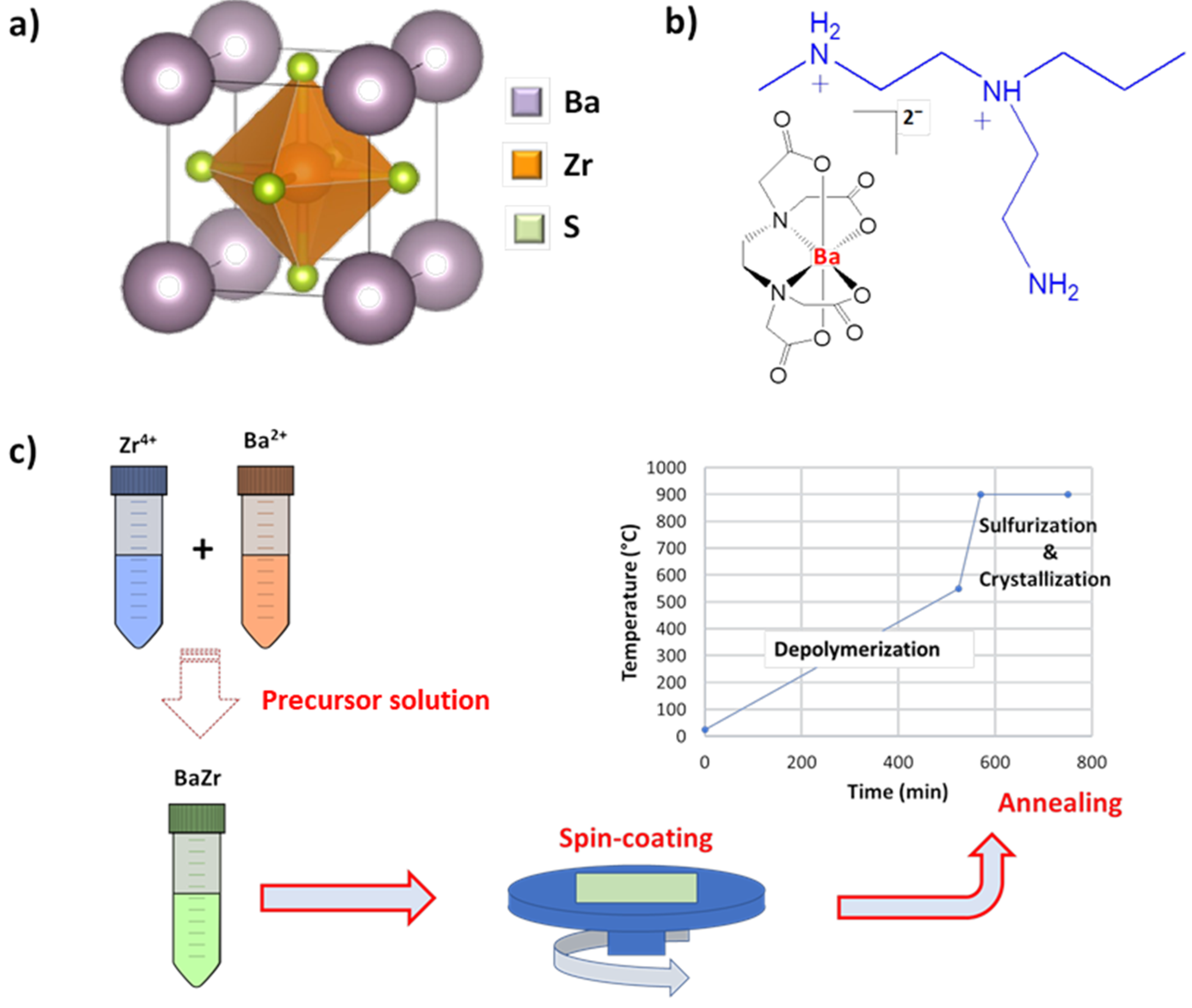
2.1. Precursor Synthesis and BZS Film Growth

The chemistry and detailed procedures to prepare aqueous precursors by PAD can be found in the relevant articles [43,44,45,46]. The solution of cation Zr4+ bound with polymer was prepared by adding 8.4 g of ZrCl4 slowly into a flacon tube containing 15 g of PEI aqueous solution (50 wt%) from Acros Organics™ (Geel, Belgium). The solution was further diluted by adding 32 mL of ultrapure water, where the solution was stirred continuously until it was clear. The solution was filtered by Amicon™ ultrafiltration with a PM 10 membrane. Inductively coupled plasma-atomic emission spectroscopy (ICP-ES) showed that the final solution had a Zr4+ cation concentration of 106 mM. ICP-ES analysis was conducted using Thermo Scientific iCAP 6000 Inductively Coupled Plasma Optical Emission Spectrometer. Detailed procedures to conduct ICP-ES analysis are presented in the Supplementary Information.
Similarly, the solution of cation Ba2+ bound with polymer PEI was prepared by adding 1.52 g of Ba(NO3)2 into a clear solution of 1.7 g of EDTA and 1.7 g of PEI (50 wt% a.q.) in 25 mL of ultrapure water. ICP-ES analysis after purification by Amicon filtration showed that the final solution had a Ba2+ cation concentration of 143 mM. It is noted that filtration used in the PAD process enables the removal of non-coordinated cations and anions [44,45,46], preventing precipitation, and therefore, yielding a homogeneous solution at the molecular level for a homogeneous coating.
The final precursor solution used for spin coating was prepared by mixing the individual cation precursors in proportion to maintain 1:1 stoichiometry by taking 0.5 mL of the Ba-PEI solution and 0.67 mL of the Zr-PEI solution to obtain 1.17 mL of 61 mM solution with respect to the Ba and Zr cations. This polymer-chelated cation solution was spin-coated on plasma-treated c-cut sapphire substrates at 6000 rpm for 60 s. The coated substrates were then thermally treated in a quartz tube furnace that was purged with Ar and kept under a continuous argon flow. To depolymerize the polymers in the as-coated precursor films and to avoid the formation of bubbles on the film surface and voids in the bulk of the films, the furnace was heated to 550 °C at a rate of 1 °C/min. The samples were then ramped (50 °C/min) to a temperature of 900 °C, and we held at this temperature for three hours under the flow of CS2 carried by Ar gas at 30 standard cubic centimeters per min. The annealing process is schematically illustrated in Figure 1c. The furnace was allowed to cool to room temperature naturally by turning off the power supply to the furnace after the thermal treatment process. The annealing temperature was chosen to ensure the decomposition of CS2 to enable the proper sulfurization of the thin films.

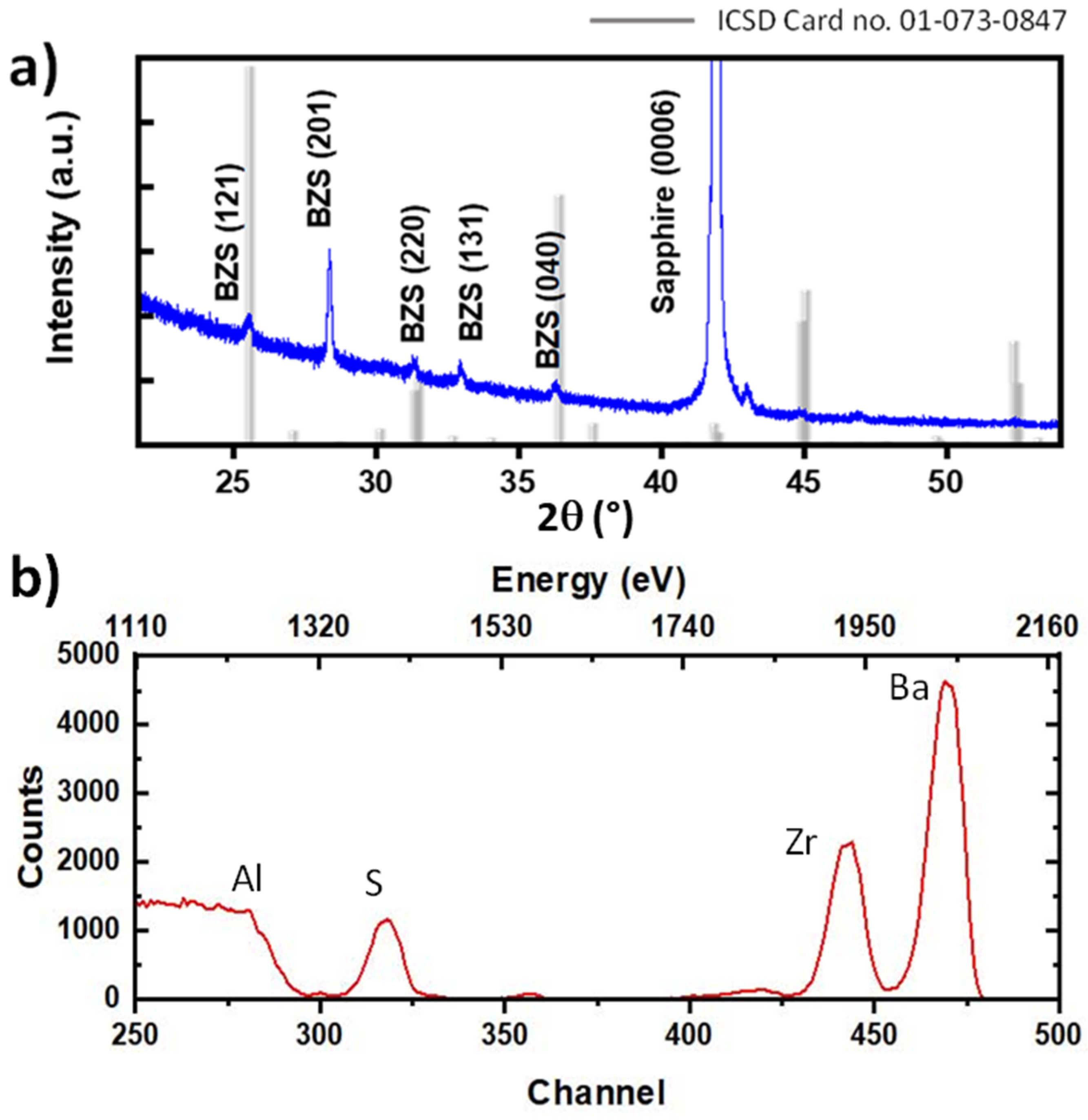
2.2. Characterization of Structure and Chemical Composition of the BZS Films

The structure of the BZS films after sulfurization in a CS2-Ar atmosphere was characterized by X-ray diffraction (XRD) using an X’Pert PANalytical MRD PRO X-ray diffractometer with Cu Ka radiation (λ = 1.54 Å). The surface morphology of the films was inspected by scanning electron microscopy (SEM) using a Focused Ion Beam Scanning Electron Microscope (FIB-SEM)—Carl Zeiss AURIGA CrossBeam with an Oxford energy-dispersive X-ray system. The chemical composition of the films was characterized by Rutherford backscattering spectrometry (RBS) and energy-dispersive X-ray spectroscopy. The RBS was conducted on a 3 MV NEC Pelletron tandem accelerator at Los Alamos National Laboratory. The 2.3 MeV 4He+ was used to maximize the mass resolution without getting into the non-Rutherford cross-section region for elements in the film and substrate. A silicon surface barrier detector was mounted at 167 degrees in reference to the beam direction to collect backscattered He particles. The total accumulated charge used was 2 μC.

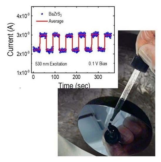
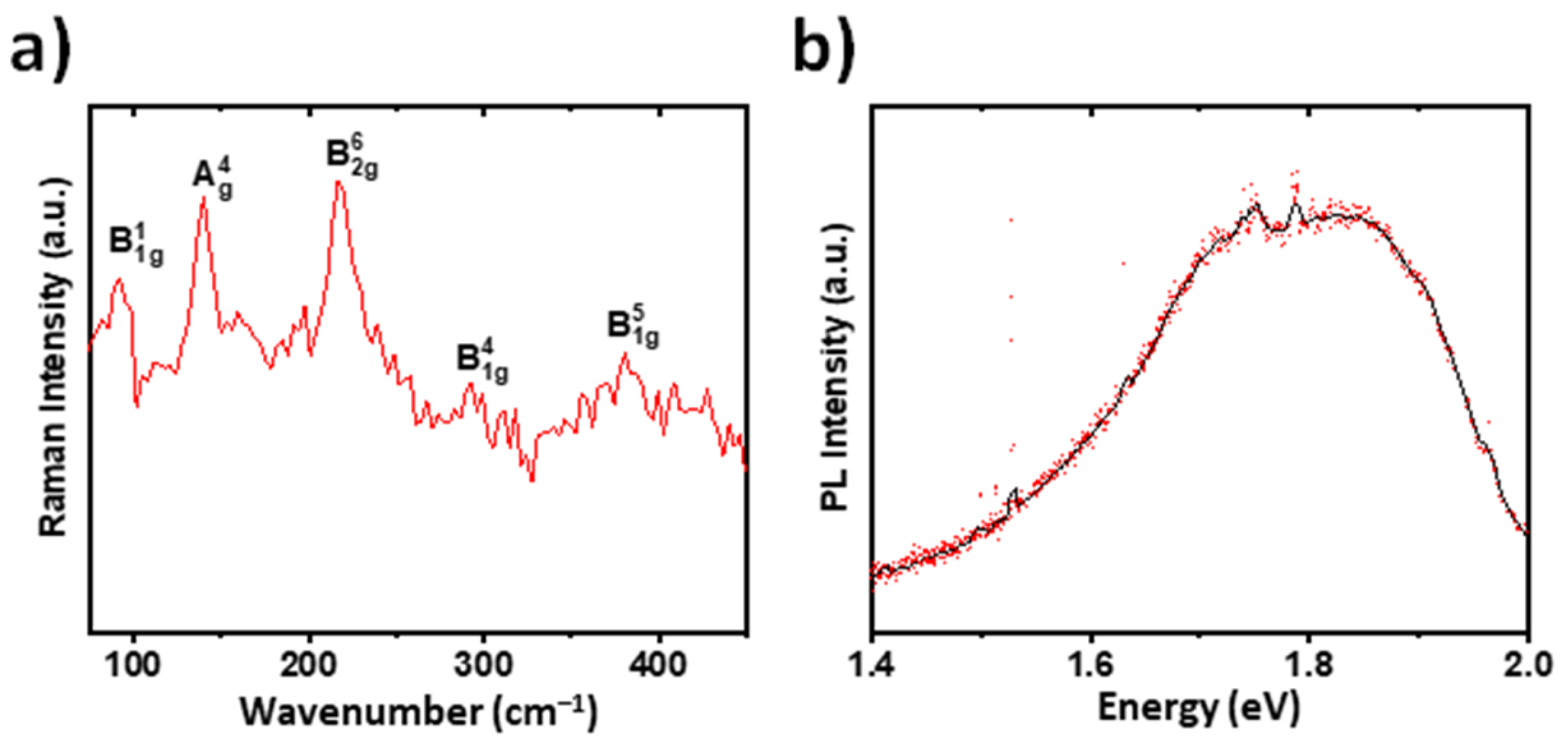
2.3. Raman Spectra, Photoluminescence, and Photocurrent Measurements of the BZS Films

Room-temperature Raman and Photoluminescence (PL) spectra of the BZS films were measured using a Renishaw inVia Raman microscope with a 1200 L/mm grating and 50× objective lens. The laser wavelength was 514 nm for the Raman and the PL spectra measurements.
To measure the photocurrent of the BZS films, uniform illumination from a 530 nm precision light-emitting diode (LED) spotlight (Mightex, Toronto, ON, Canada) with an output power of about 38 mW was shined on the surface of the films. The light source provides a uniform illumination spot with a diameter of 22 mm at a working distance of 10 cm from the surface of the BZS sample. The photocurrent measurements were taken using an Agilent E4890 precision LCR meter with an applied DC bias of 100 mV on the sample surface.

2.4. Temperature-Dependence of Resistance Measurements

The temperature-dependent resistance of the BZS samples was measured using the direct current resistance setup in a Physical Property Measurement System (PPMS, Quantum Design). A square shape sample was wired in a four-probe geometry using indium metal wires with a direct current applied through two of the probes, while the other two probes were used to measure the voltage.

3. Results

As can be seen from Figure 2, the XRD θ-2θ scans show the formation of single-phase polycrystalline perovskite BaZrS3 film on the c-plane sapphire substrate. All the discernible diffraction peaks of the film match well with the standard peak positions of BZS, where the BZS is crystallized in a distorted perovskite structure of the orthorhombic Pnma space group retrieved from the PDF (powder diffraction file) card ICDD 00-015-0327. No additional peaks were observed, suggesting that the films synthesized by PAD were phase pure chalcogenide perovskite. The surface of BZS films processed at such an annealing temperature showed the morphology of a connected network of crystals (see Figure S1, Supplementary Information). The composition of the as-fabricated films was determined by Rutherford backscattering spectrometry (RBS). The atomic ratios were determined to be 1:1.03:3.02 (within 5% errors), which is very similar to the ideal Ba:Zr:S ratio of 1:1:3. It is noted that the atomic ratio measured from an energy-dispersive X-ray is similar to the compositions obtained by RBS (see Figure S2, Supplementary Information). The BZS film thickness was estimated to be 83 nm from the fitting to the RBS spectrum. This value was very similar to the film thickness (~76 nm) estimated from the XRD full width at the half maximum (~0.112°) of the BZS (201) diffraction peak.
The Raman spectrum of the BZS film synthesized by PAD is illustrated in Figure 3a. Five major peaks can be observed between wavenumbers 50 and 400 cm−1, which are identified as B 1 g 1 , A g 4 , B 2 g 6 ,   B 1 g 4 , and B 1 g 5 modes. As illustrated in Figure 3b, the PL spectrum of the film shows a broad peak centered around 1.8 eV, with a width of ~200 meV. Both the Raman and PL measurements of the BZS films prepared by PAD are in good agreement with prior reports of BaZrS3 with the Pnma structure [17,22,26,47,48,49].
The BZS films synthesized by PAD show a noticeable photogenerated current, as illustrated in Figure 4a. Given that the bandgap of BZS is at around 1.8 eV, we used a 530 nm LED to illuminate the BZS film. Figure 4a shows the time-dependent current of the BZS film by turning the LED on and off, where the BZS film was biased at 0.1 V at room temperature in the dark. As can be seen from Figure 4a, an increase in the current was detected due to the photogenerated carriers in the BZS film under illumination.
The temperature-dependent electrical resistivity of BZS samples is shown in Figure 4b. The increase in resistivity with decreasing temperature suggests the film behaves as a semiconductor does. Beyond 60 K, the resistance value exceeded the measurement limit of our PPMS setup. The non-linear nature of the resistivity vs. temperature characteristic may come from two distinct carrier transport mechanisms. In semiconductors, the conductivity (or resistivity) is normally governed by thermally activated carriers (electron or hole) at room temperature, where the thermally activated electrical conductivity of semiconducting materials is often described by the Arrhenius relation,
σ = σ 0 e x p ( E a k T )
where σ0 is a constant, Ea is the activation energy, and k is Boltzmann’s constant. The electrical resistivity of a material can be expressed as R = 1 σ l A , where σ is the electrical conductivity (reciprocal of electrical resistivity), l is the length of the sample, and A is the cross-sectional area through which the carrier transport is taking place. By replacing σ with 1 R l A , the modified version of the Arrhenius equation can be written as l n 1 R = ( E a k ) 1 T + l n ( 1 R 0 ) , where R0 is a constant. The ln(1/R) vs. 1/T plot should exhibit a linear relationship with a slope of −(Ea/k) and an intercept of ln(1/R0) if thermally activated Arrhenius-type conduction dominates the conductivity. As shown in Figure 4c, the linear relationship of ln(1/R) vs. 1/T between 300 K and 220 K suggests the thermally activated conduction in the range of the mentioned temperatures. The calculated activation energy for the sample is about 44 meV, which is higher than that of the BZS films previously reported via the sulfurization of BaZrO3 films [22]. The highly resistive nature of the BZS film synthesized by PAD suggests a relatively lower carrier concentration that is directly related to the activation energy at a given temperature. At a temperature lower than 220 K, Figure 4c clearly shows that the fitting starts deviating from the linear relationship of ln(1/R) vs. 1/T. This deviation suggests a different conduction mechanism in the low-temperature region for the BZS films synthesized by PAD. In the low-temperature region, we find that the Efros–Shklovskii (E-S)-type variable range hopping model can be used to fit the experimental data, as shown in Figure 4d. This model can be expressed with the following equation [50],
σ E S ( T ) = σ 0 E S T e x p T E S T 1 / 2
where the E-S model takes into account the coulomb interactions between the localized electrons at lower temperatures. The characteristic temperature, TES, depends on the localization length and dielectric constant of the material. As can be seen from Figure 4d, our experimental data can be best fitted by a linear relationship between ln(T/R) and 1 / T 1 / 2 at temperatures below 220 K. The conductivity of BZS film synthesized by PAD at low temperatures is consistent with the previously reported charge transport mechanism in BZS films derived from the sulfurization of BaZrO3 films [22]. Further systematic studies are needed to identify and quantify the role of crystallinity and stoichiometry of the BZS thin films on optoelectronic properties derived from various growth techniques.

4. Conclusions

This work sets the stage for developing chalcogenide perovskites as a family of semiconductor materials using a benign aqueous chemical solution deposition method, i.e., polymer-assisted deposition. The polycrystalline BaZrS3 films synthesized by polymer-assisted deposition show photoluminescence and photo-generated currents similar to those of the polycrystalline BaZrS3 films deposited by physical vapor deposition. The charge transport of the demonstrated film was ascertained to follow the E-S variable range hopping at lower temperatures and Arrhenius thermally activated conduction at temperatures above 220 K to room temperature. The growth of chalcogenide perovskite BaZrS3 films by a polymer-assisted deposition not only provides an attractive synthetic route for the deposition of such a class of semiconductor materials, but it also offers the potential to impact research on other sulfur- and selenium-containing chalcogenide compounds.

Supplementary Materials

The following supporting information can be downloaded at: https://www.mdpi.com/article/10.3390/photonics10040366/s1, Figure S1: SEM image of BaZrS3 film deposited by polymer-assisted deposition, where the precursor film was annealed at 900 °C. Figure S2: Energy-dispersive X-ray spectrum of a BaZrS3 film grown by polymer-assisted deposition.

Author Contributions

Conceptualization: S.D. and Q.J.; methodology: S.D., X.W., P.R., Z.C., H.H. and Y.W.; investigation, S.D., P.R., Z.C., Y.W., W.N., A.C., H.Z. and Q.J.; Writing: original draft preparation, S.D. and Q.J.; writing—review and editing: S.D., X.W., H.H., P.R., Z.C., Y.W., A.C., W.N., H.Z. and Q.J.; supervision: Q.J. All authors have read and agreed to the published version of the manuscript.

Funding

This research at the University at Buffalo was funded by the U.S. National Science Foundation under award numbers ECCS-1902623 and ECCS-2042085. The research at Los Alamos National Laboratory was supported by the NNSA’s Laboratory Directed Research and Development Program, managed by Triad National Security, LLC for the U.S. Department of Energy’s NNSA, under contract 89233218CNA000001.

Institutional Review Board Statement

Not applicable.

Informed Consent Statement

Not applicable.

Data Availability Statement

The data that support the findings of this study are available from the corresponding author upon reasonable request.

Acknowledgments

The work at the University at Buffalo was partially supported by the U.S. National Science Foundation under award numbers ECCS-1902623 and ECCS-2042085. The work at Los Alamos National Laboratory was supported by the NNSA’s Laboratory Directed Research and Development Program. Los Alamos National Laboratory, an affirmative action equal opportunity employer managed by Triad National Security, LLC, for the U.S. Department of Energy’s, NNSA, under contract 89233218CNA000001. The work at Los Alamos National Laboratory was performed, in part, at the Center for Integrated Nanotechnologies (CINT), an Office of Science User Facility operated by the U.S. Department of Energy Office of Science. S.D., P.R., Z.C., and Q.J. acknowledge the CINT Users Program.

Conflicts of Interest

The authors declare no conflict of interest. The funders had no role in the design of the study; in the collection, analyses, or interpretation of data; in the writing of the manuscript; or in the decision to publish the results.

References

  1. Peña, M.A.; Fierro, J.L.G. Chemical Structures and Performance of Perovskite Oxides. Chem. Rev. 2001, 101, 1981–2018. [Google Scholar] [CrossRef]
  2. Bresolin, B.-M.; Park, Y.; Bahnemann, D.W. Recent Progresses on Metal Halide Perovskite-Based Material as Potential Photocatalyst. Catalysts 2020, 10, 709. [Google Scholar] [CrossRef]
  3. Hwang, J.; Rao, R.R.; Giordano, L.; Katayama, Y.; Yu, Y.; Shao-Horn, Y. Perovskites in catalysis and electrocatalysis. Science 2017, 358, 751–756. [Google Scholar] [CrossRef]
  4. Rondinelli, J.M.; May, S.J.; Freeland, J.W. Control of octahedral connectivity in perovskite oxide heterostructures: An emerging route to multifunctional materials discovery. MRS Bull. 2012, 37, 261–270. [Google Scholar] [CrossRef]
  5. Raveau, B.; Maignan, A.; Martin, C.; Hervieu, M. Colossal Magnetoresistance Manganite Perovskites: Relations between Crystal Chemistry and Properties. Chem. Mater. 1998, 10, 2641–2652. [Google Scholar] [CrossRef]
  6. Bednorz, J.G.; Müller, K.A. Perovskite-type oxides—The new approach to high-Tcsuperconductivity. Rev. Mod. Phys. 1988, 60, 585–600. [Google Scholar] [CrossRef]
  7. Tress, W. Metal Halide Perovskites as Mixed Electronic–Ionic Conductors: Challenges and Opportunities—From Hysteresis to Memristivity. J. Phys. Chem. Lett. 2017, 8, 3106–3114. [Google Scholar] [CrossRef]
  8. Dhole, S.; Chen, A.; Nie, W.; Park, B.; Jia, Q. Strain Engineering: A Pathway for Tunable Functionalities of Perovskite Metal Oxide Films. Nanomaterials 2022, 12, 835. [Google Scholar] [CrossRef]
  9. Burschka, J.; Pellet, N.; Moon, S.-J.; Humphry-Baker, R.; Gao, P.; Nazeeruddin, M.K.; Grätzel, M. Sequential deposition as a route to high-performance perovskite-sensitized solar cells. Nature 2013, 499, 316–319. [Google Scholar] [CrossRef] [PubMed]
  10. Zhu, Y.; Liu, Y.; Ai, Q.; Gao, G.; Yuan, L.; Fang, Q.; Tian, X.; Zhang, X.; Egap, E.; Ajayan, P.M.; et al. In Situ Synthesis of Lead-Free Halide Perovskite–COF Nanocomposites as Photocatalysts for Photoinduced Polymerization in Both Organic and Aqueous Phases. ACS Mater. Lett. 2022, 4, 464–471. [Google Scholar] [CrossRef]
  11. Zhu, Y.; Liu, Y.; Miller, K.A.; Zhu, H.; Egap, E. Lead Halide Perovskite Nanocrystals as Photocatalysts for PET-RAFT Polymerization under Visible and Near-Infrared Irradiation. ACS Macro Lett. 2020, 9, 725–730. [Google Scholar] [CrossRef] [PubMed]
  12. Liu, M.; Xia, P.; Zhao, G.; Nie, C.; Gao, K.; He, S.; Wang, L.; Wu, K. Energy-Transfer Photocatalysis Using Lead Halide Perovskite Nanocrystals: Sensitizing Molecular Isomerization and Cycloaddition. Angew. Chem. Int. Edit. 2022, 61, e202208241. [Google Scholar]
  13. Sun, Y.-Y.; Agiorgousis, M.L.; Zhang, P.; Zhang, S. Chalcogenide Perovskites for Photovoltaics. Nano Lett. 2015, 15, 581–585. [Google Scholar] [CrossRef]
  14. Zilevu, D.; Creutz, S.E. Shape-Controlled Synthesis of Colloidal Nanorods and Nanoparticles of Barium Titanium Sulfide. Chem. Mater. 2021, 33, 5137–5146. [Google Scholar] [CrossRef]
  15. Adjogri, S.J.; Meyer, E.L. Chalcogenide Perovskites and Perovskite-Based Chalcohalide as Photoabsorbers: A Study of Their Properties, and Potential Photovoltaic Applications. Materials 2021, 14, 7857. [Google Scholar] [CrossRef]
  16. Sharma, S.; Ward, Z.; Bhimani, K.; Li, K.; Lakhnot, A.; Jain, R.; Shi, S.-F.; Terrones, H.; Koratkar, N. Bandgap Tuning in BaZrS3 Perovskite Thin Films. ACS Appl. Electron. Mater. 2021, 3, 3306–3312. [Google Scholar] [CrossRef]
  17. Yu, Z.; Wei, X.; Zheng, Y.; Hui, H.; Bian, M.; Dhole, S.; Seo, J.-H.; Sun, Y.-Y.; Jia, Q.; Zhang, S.; et al. Chalcogenide perovskite BaZrS3 thin-film electronic and optoelectronic devices by low temperature processing. Nano Energy 2021, 85, 105959. [Google Scholar] [CrossRef]
  18. Wu, X.; Gao, W.; Chai, J.; Ming, C.; Chen, M.; Zeng, H.; Zhang, P.; Zhang, S.; Sun, Y.-Y. Defect tolerance in chalcogenide perovskite photovoltaic material BaZrS3. Sci. China Mater. 2021, 64, 2976–2986. [Google Scholar] [CrossRef]
  19. Surendran, M.; Chen, H.; Zhao, B.; Thind, A.S.; Singh, S.; Orvis, T.; Zhao, H.; Han, J.-K.; Htoon, H.; Kawasaki, M.; et al. Epitaxial Thin Films of a Chalcogenide Perovskite. Chem. Mater. 2021, 33, 7457–7464. [Google Scholar] [CrossRef]
  20. Osei-Agyemang, E.; Koratkar, N.; Balasubramanian, G. Examining the electron transport in chalcogenide perovskite BaZrS3. J. Mater. Chem. C 2021, 9, 3892–3900. [Google Scholar] [CrossRef]
  21. Nishigaki, Y.; Nagai, T.; Nishiwaki, M.; Aizawa, T.; Kozawa, M.; Hanzawa, K.; Kato, Y.; Sai, H.; Hiramatsu, H.; Hosono, H.; et al. Extraordinary Strong Band-Edge Absorption in Distorted Chalcogenide Perovskites. Sol. RRL 2020, 4, 1900555. [Google Scholar] [CrossRef]
  22. Wei, X.; Hui, H.; Zhao, C.; Deng, C.; Han, M.; Yu, Z.; Sheng, A.; Roy, P.; Chen, A.; Lin, J.; et al. Realization of BaZrS3 chalcogenide perovskite thin films for optoelectronics. Nano Energy 2019, 68, 104317. [Google Scholar] [CrossRef]
  23. Pandey, J.; Ghoshal, D.; Dey, D.; Gupta, T.; Taraphder, A.; Koratkar, N.; Soni, A. Local ferroelectric polarization in antiferroelectric chalcogenide perovskite BaZrS3 thin films. Phys. Rev. B 2020, 102, 205308. [Google Scholar] [CrossRef]
  24. Zitouni, H.; Tahiri, N.; El Bounagui, O.; Ez-Zahraouy, H. Electronic, optical and transport properties of perovskite BaZrS3 compound doped with Se for photovoltaic applications. Chem. Phys. 2020, 538, 110923. [Google Scholar] [CrossRef]
  25. Filippone, S.; Zhao, B.; Niu, S.; Koocher, N.Z.; Silevitch, D.; Fina, I.; Rondinelli, J.M.; Ravichandran, J.; Jaramillo, R. Discovery of highly polarizable semiconductors BaZrS3 and Ba3Zr2S7. Phys. Rev. Mater. 2020, 4, 091601. [Google Scholar] [CrossRef]
  26. Wei, X.; Hui, H.; Perera, S.; Sheng, A.; Watson, D.F.; Sun, Y.-Y.; Jia, Q.; Zhang, S.; Zeng, H. Ti-Alloying of BaZrS3 Chalcogenide Perovskite for Photovoltaics. ACS Omega 2020, 5, 18579–18583. [Google Scholar] [CrossRef]
  27. Niu, S.; Zhao, B.; Ye, K.; Bianco, E.; Zhou, J.; McConney, M.E.; Settens, C.; Haiges, R.; Jaramillo, R.; Ravichandran, J. Crystal growth and structural analysis of perovskite chalcogenide BaZrS3 and Ruddlesden–Popper phase Ba3Zr2S7. J. Mater. Res. 2019, 34, 3819–3826. [Google Scholar] [CrossRef]
  28. Peng, Y.; Sun, Q.; Chen, H.; Yin, W.-J. Disparity of the Nature of the Band Gap between Halide and Chalcogenide Single Perovskites for Solar Cell Absorbers. J. Phys. Chem. Lett. 2019, 10, 4566–4570. [Google Scholar] [CrossRef]
  29. Agiorgousis, M.L.; Sun, Y.; Choe, D.; West, D.; Zhang, S. Machine Learning Augmented Discovery of Chalcogenide Double Perovskites for Photovoltaics. Adv. Theory Simul. 2019, 2, 1800173. [Google Scholar] [CrossRef]
  30. Niu, S.; Milam-Guerrero, J.; Zhou, Y.; Ye, K.; Zhao, B.; Melot, B.C.; Ravichandran, J. Thermal stability study of transition metal perovskite sulfides. J. Mater. Res. 2018, 33, 4135–4143. [Google Scholar] [CrossRef]
  31. Meng, W.; Saparov, B.; Hong, F.; Wang, J.; Mitzi, D.B.; Yan, Y. Alloying and Defect Control within Chalcogenide Perovskites for Optimized Photovoltaic Application. Chem. Mater. 2016, 28, 821–829. [Google Scholar] [CrossRef]
  32. Xu, J.; Fan, Y.; Tian, W.; Ye, L.; Zhang, Y.; Tian, Y.; Han, Y.; Shi, Z. Enhancing the optical absorption of chalcogenide perovskite BaZrS3 by optimizing the synthesis and post-processing conditions. J. Solid State Chem. 2022, 307, 122872. [Google Scholar] [CrossRef]
  33. Gupta, T.; Ghoshal, D.; Yoshimura, A.; Basu, S.; Chow, P.K.; Lakhnot, A.S.; Pandey, J.; Warrender, J.M.; Efstathiadis, H.; Soni, A.; et al. An Environmentally Stable and Lead-Free Chalcogenide Perovskite. Adv. Funct. Mater. 2020, 30, 2001387. [Google Scholar] [CrossRef]
  34. Ravi, V.K.; Yu, S.H.; Rajput, P.K.; Nayak, C.; Bhattacharyya, D.; Chung, D.S.; Nag, A. Colloidal BaZrS3 chalcogenide perovskite nanocrystals for thin film device fabrication. Nanoscale 2020, 13, 1616–1623. [Google Scholar] [CrossRef]
  35. Márquez, J.A.; Rusu, M.; Hempel, H.; Ahmet, I.Y.; Kölbach, M.; Simsek, I.; Choubrac, L.; Gurieva, G.; Gunder, R.; Schorr, S.; et al. BaZrS3 Chalcogenide Perovskite Thin Films by H2S Sulfurization of Oxide Precursors. J. Phys. Chem. Lett. 2021, 12, 2148–2153. [Google Scholar] [CrossRef]
  36. Sadeghi, I.; Ye, K.; Xu, M.; Li, Y.; LeBeau, J.M.; Jaramillo, R. Making BaZrS3 Chalcogenide Perovskite Thin Films by Molecular Beam Epitaxy. Adv. Funct. Mater. 2021, 31, 202105563. [Google Scholar] [CrossRef]
  37. Filippone, S.; Song, S.; Jaramillo, R. High densification of BaZrS3 powder inspired by the cold-sintering process. J. Mater. Res. 2021, 36, 4404–4412. [Google Scholar] [CrossRef]
  38. Comparotto, C.; Davydova, A.; Ericson, T.; Riekehr, L.; Moro, M.V.; Kubart, T.; Scragg, J.J.S. Chalcogenide Perovskite BaZrS3: Thin Film Growth by Sputtering and Rapid Thermal Processing. ACS Appl. Energy Mater. 2020, 3, 2762–2770. [Google Scholar] [CrossRef]
  39. Yang, R.; Jess, A.D.; Fai, C.; Hages, C.J. Low-Temperature, Solution-Based Synthesis of Luminescent Chalcogenide Perovskite BaZrS3 Nanoparticles. J. Am. Chem. Soc. 2022, 144, 15928–15931. [Google Scholar] [CrossRef]
  40. Luo, H.; Wang, H.; Zou, G.; Bauer, E.; Mccleskey, T.M.; Burrell, A.K.; Jia, Q. A Review of Epitaxial Metal-Nitride Films by Polymer-Assisted Deposition. Trans. Electr. Electron. Mater. 2010, 11, 54–60. [Google Scholar] [CrossRef]
  41. Zou, G.; Wang, H.; Mara, N.; Luo, H.; Li, N.; Di, Z.; Bauer, E.; Wang, Y.; McCleskey, T.; Burrell, A.; et al. Chemical Solution Deposition of Epitaxial Carbide Films. J. Am. Chem. Soc. 2010, 132, 2516–2517. [Google Scholar] [CrossRef] [PubMed]
  42. Luo, H.; Lin, Y.; Wang, H.; Lee, J.H.; Suvorova, N.A.; Mueller, A.H.; Burrell, A.K.; McCleskey, T.M.; Bauer, E.; Usov, I.O.; et al. A Chemical Solution Approach to Epitaxial Metal Nitride Thin Films. Adv. Mater. 2009, 21, 193–197. [Google Scholar] [CrossRef]
  43. Burrell, A.K.; McCleskey, T.M.; Jia, Q.X. Polymer assisted deposition. Chem. Commun. 2008, 1271–1277. [Google Scholar] [CrossRef]
  44. Jia, Q.X.; Mccleskey, T.; Burrell, A.K.; Lin, Y.; Collis, G.E.; Wang, H.; Li, A.D.Q.; Foltyn, S.R. Polymer-assisted deposition of metal-oxide films. Nat. Mater. 2004, 3, 529–532. [Google Scholar] [CrossRef] [PubMed]
  45. McCleskey, T.M.; Shi, P.; Bauer, E.; Highland, M.J.; Eastman, J.A.; Bi, Z.X.; Fuoss, P.H.; Baldo, P.M.; Ren, W.; Scott, B.L.; et al. Nucleation and growth of epitaxial metal-oxide films based on polymer-assisted deposition. Chem. Soc. Rev. 2013, 43, 2141–2146. [Google Scholar] [CrossRef]
  46. Zou, G.F.; Zhao, J.; Luo, H.M.; McCleskey, T.M.; Burrell, A.K.; Jia, Q.X. Polymer-assisted-deposition: A chemical solution route for a wide range of materials. Chem. Soc. Rev. 2012, 42, 439–449. [Google Scholar] [CrossRef]
  47. Perera, S.; Hui, H.; Zhao, C.; Xue, H.; Sun, F.; Deng, C.; Gross, N.; Milleville, C.; Xu, X.; Watson, D.F.; et al. Chalcogenide perovskites—An emerging class of ionic semiconductors. Nano Energy 2016, 22, 129–135. [Google Scholar] [CrossRef]
  48. Gross, N.; Sun, Y.-Y.; Perera, S.; Hui, H.; Wei, X.; Zhang, S.; Zeng, H.; Weinstein, B.A. Stability and Band-Gap Tuning of the Chalcogenide Perovskite BaZrS3 in Raman and Optical Investigations at High Pressures. Phys. Rev. Appl. 2017, 8, 044014. [Google Scholar] [CrossRef]
  49. Niu, S.; Huyan, H.; Liu, Y.; Yeung, M.; Ye, K.; Blankemeier, L.; Orvis, T.; Sarkar, D.; Singh, D.J.; Kapadia, R.; et al. Bandgap Control via Structural and Chemical Tuning of Transition Metal Perovskite Chalcogenides. Adv. Mater. 2016, 29, 201604733. [Google Scholar] [CrossRef]
  50. Efros, A.L.; Shklovskii, B.I. Coulomb gap and low temperature conductivity of disordered systems. J. Phys. C Solid State Phys. 1975, 8, L49–L51. [Google Scholar] [CrossRef]
Figure 1. Schematic illustrations of (a) crystal structure of perovskite BaZrS3, (b) the polymer (such as PEI) in the solution binds to the metal ions (such as Ba) through electrostatic attraction, hydrogen bonding, and/or covalent bonding, and (c) the major stages of PAD deposition process to synthesize BaZrS3 films.
Photonics 10 00366 g001
Figure 2. (a) XRD θ 2 θ scan of the as prepared single phase BZS thin film synthesized by a polymer-assisted deposition, where the experimental data are shown in blue, and the peak positions from PDF card ICDD 01-073-0847 are shown as stick patterns in gray. The high intensity peak corresponds to the (0006) c-plane sapphire substrate. (b) RBS spectra (2.3 MeV 4He+) of the as prepared BZS film. The film thickness was estimated to be 83 nm. The atomic ratio of Ba:Zr:S was found to be 1.00:1.03:3.02 by fitting the RBS spectra. Small amount of other elements such as Ar (355 channel) and potentially Zn or Cu (418 channel) from the RBS spectrum may come from the contamination during the process. The atomic ratios are within 5% errors based on RBS analysis.
Photonics 10 00366 g002
Figure 3. (a) Raman and (b) PL spectra of the BaZrS3 film measured at 300 K. The sharp spikes from the PL spectra come from the sapphire substrate. The black line shows the smoothed curve derived from the average of the experimental results.
Photonics 10 00366 g003
Figure 4. (a) Photogenerated current of BZS films illuminated by an LED at an excitation wavelength of 530 nm, an output power of about 38 mW, and 0.1 V bias measured at room temperature. (b) Temperature dependence of resistivity measured using a four-probe configuration. (c) Linear fit of the experimental data using an Arrhenius model. A divergence of the fitting starts at a temperature lower than 220 K. (d) Linear fit of experimental data using an E-S variable range hopping model at temperatures lower than 220 K. The red and green circles are used to show the experimental data at temperatures above and below 220 K, respectively.
Photonics 10 00366 g004
Disclaimer/Publisher’s Note: The statements, opinions and data contained in all publications are solely those of the individual author(s) and contributor(s) and not of MDPI and/or the editor(s). MDPI and/or the editor(s) disclaim responsibility for any injury to people or property resulting from any ideas, methods, instructions or products referred to in the content.

