1. Introduction
The demand for the miniaturization and topological complexity of devices in scientific research and industrial applications promotes the development of three-dimensional (3D) manufacturing to the micro- and nanoscale. As one of the primary technologies in direct laser writing (DLW), two-photon lithography (TPL) [
1] allows for flexible modifications of manufacture patterns without the need for a mask, significantly accelerating the optimization of the structural design. A femtosecond pulse laser is focused tightly on the interface between the substrate and photopolymer resin by a microscopic objective lens. Only the excitation intensity close to the focal point may exceed the absorption threshold of the resin and cause it to cure due to the nonlinearity of two-photon absorption (TPA). Therefore, TPL breaks the diffraction limit at excitation wavelength by obtaining double photon energy, resulting in the high resolution of the submicron order. Meanwhile, TPL has greater laser penetration depth and less photobleaching compared with the DLW technology based on one-photon absorption (OPA). Thanks to its high flexibility, resolution, and low working environment requirements, TPL is widely utilized to fabricated tiny and complex structures with submicron resolution, such as functional materials [
2], micro-optical components [
3], cell mechanobiology [
4], and so on [
5,
6,
7]. Although high numerical aperture (NA) objective lenses are usually used to reduce the diffraction effects and narrow the linewidths in TPL, the depth of field (DOF) is also reduced dramatically at the same time. During the manufacturing process, the focal spot must remain on the substrate’s surface with nanometer precision to ensure the stable adherence of the cured resin to the substrate. Therefore, the autofocus system becomes indispensable, especially for long-term manufacturing and large-scale fabrication in practical applications.
To overcome the defocus of the substrate caused by a variety of factors (e.g., thermal drift, mechanical vibrations, and the tilt of the substrate surface), some autofocus technologies have been proposed in the lithography systems. Though image-based methods simplify the experimental setup, the focusing accuracy is not satisfactory and is sensitive to image quality [
8,
9,
10,
11]. The active methods rely on the modulation of the light beam from the additional laser source. The defocus amount of the substrate can be measured by detecting the change in light spot characteristics on the detector. Liu et al. developed an autofocus microscope with the centroid method and added another optical path to enlarge the linear autofocus range [
12]. Then, the focusing accuracy was improved by changing some optical elements and the measurement method [
13,
14]. In addition, various masks were employed to reshape the light beam incident to the objective lens [
15,
16,
17,
18]. For example, Du et al. combined a quarter baffle and an annular diffractive optical element (DOE) to achieve a defocus detection accuracy of 100 nm and a detection range of more than 76
[
15]. Moreover, the astigmatic strategy is also popular in defocus detection. Bai et al. utilized the double cylinder lens group to reshape the light spot on the four-quadrant detector (FQD) and analyzed the defocus variation with an accuracy of 50 nm within a 18
range [
19]. To decrease the impact of noise and instability, Du et al. proposed a differential astigmatic method [
20], improving the system detection accuracy to 30 nm. For the TPL system with a high NA (such as 1.45) microscopic objective lens, the DOF is less than 100 nm at the excitation wavelength of
λ = 532 nm [
19], putting forward stricter requirements for focusing accuracy. Furthermore, the previous high-precision autofocus methods were mainly verified on high-reflectivity substrates, such as mirrors and silicon. However, for the fabrication of the transmissive DOE (which is based on a silica substrate), the reflected signal from the interface is extremely faint and is attributed to the tiny refractive index difference (about 0.01) between the substrate and photoresist, resulting in the significant reduction in signal-to-noise ratio (SNR) and detection accuracy of autofocus. Therefore, the defocus detection methods with higher accuracy that can be used on the low-reflectivity substrates should be considered.
Accounting for the steep slope of the axial response curve of the confocal system with a high NA objective, the improved differential confocal microscopy (IDCM) is a good choice for high-precision defocus measurement. As an improvement of conventional confocal microscopy (CM), IDCM is able to describe the position of the sample relative to the objective lens easily by analyzing the intensity response signals obtained from two detectors, which are located symmetrically in front of and behind the focal planes of collecting lenses [
21,
22,
23]. Benefiting from the steep slope of the axial response curve in the linear region and the unique signal processing method, it provides an excellent performance in ultra-precision measurement, simple data processing, and great noise suppression capability. Hence, it has been applied in surface profilometry [
24,
25,
26], measurement of lens radii of curvature [
27], and the autofocus in biological research [
28]. However, it has not been applied in TPL to achieve a high-precision defocus detection.
In this work, an ultra-precision autofocus method based on IDCM is proposed for the TPL system. The defocus amount and direction in the TPL process were measured by analyzing the intensity response signals that were acquired periodically. Then, refocusing was implemented with the piezoelectric transducer (PZT) platform. Two photomultiplier tubes (PMT) were selected as detectors to amplify the detection signals instead of photodiodes (PD) to improve the SNR. An autofocus setup based on IDCM was built and verification experiments were carried out on the glass coverslip. The results demonstrated high detection sensitivity (5 nm) and focusing accuracy (5 nm) for the autofocus system with a high NA objective lens. The characterization of a fabricated metalens array [
29] further proved the effectiveness of the IDCM-based autofocus system. The proposed approach provides a good way for autofocus with great advantages of high precision and good anti-noise performance and has broad application prospects for more complex structure fabrication on various substrates in TPL.
2. Autofocus Principle and Method
In conventional confocal microscopy, the axial response curve describes the relationship between the position of the sample and the light intensity signal obtained from the detector. The intensity peak of the curve corresponds to the in-focus state of the sample. Thus, focusing can be implemented by maximizing the light intensity signal on the detector. However, Lee et al. found that the maximal detection sensitivity for the axial motion of the sample appeared at the slope of the axial response curve, instead of the peak, and proposed the concept of differential confocal microscopy (DCM) [
30]. The sample can be positioned slightly away from the focal plane to reach a higher measurement precision. Zhao et al. developed the DCM technology by employing two detectors positioned before and behind the imaging focal planes [
21], which can be defined as bipolar absolute differential confocal microscopy (BADCM). The slope of the axial response curve of BADCM in the working region doubles compared with conventional DCM using a single axially offset placed detector, and it can carry out an ultra-precision bipolar absolute measurement of sample motion. Furthermore, Liu et al. came up with improved differential confocal microscopy (IDCM) to enhance the reflectance disturbance resistibility [
23].
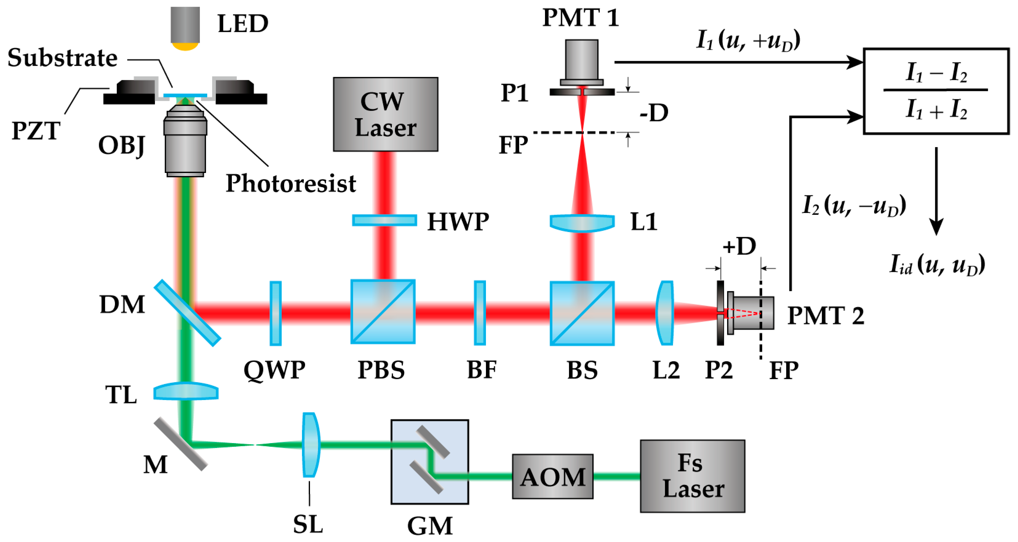
The optical diagram of the autofocus system based on IDCM is shown in
Figure 1. The light beam is emitted from a continuous wave laser (CW Laser). After polarization modulation by a half-wave plate (HWP), the beam is reflected by a polarization beam splitter (PBS). The HWP should be rotated properly to maximize the intensity of the reflected beam. Then, the beam passes through a quarter-wave plate (QWP) and is changed to circularly polarized light. Reflecting by a dichroic mirror (DM), the beam is focused on the interface between the photoresist and substrate by a microscope objective lens (OBJ). The substrate is fixed on an adapter, which is controlled by a PZT to move with nanometer precision. The reflected light at the interface is collected by the objective and passes through the QWP again, changing the polarization of the returned beam for transmission through the PBS. The bandpass filter (BF) allows only the reflected detection beam to pass through, thereby decreasing the disturbance of light from other sources in the environment. Then, the beam is equally divided into two light paths by a beam splitter (BS) and focused separately by two collective lenses (L1 and L2) with the same parameters. The pinhole1 (P1) and pinhole2 (P2) are placed behind and before the focal planes (FP) of the collective lenses, respectively, with the same distance
D, followed by the detectors PMT1 and PMT2. While the substrate is placed at the focal plane of the objective, the received light intensities of both detectors are equal. With a tiny displacement of the substrate from the focal plane, the corresponding imaging focal plane has an equivalent shift approaching one pinhole and retreating from the other, leading to the light intensity detected by one detector increasing while the other is decreasing.
While scanning the flat substrate axially through focus, the intensity response signals obtained by the point detector PMT1 and PMT2 can be expressed as [
24]
where
λ is the wavelength of the light beam;
r and
z are the lateral and axial coordinate in the object space, respectively;
is the effective numerical aperture of the objective lens;
and
u are lateral and axial normalized optical coordinates in the object space, respectively;
is the normalized optical distance corresponding to the axial offset
D of the pinhole;
and
are 3D point spread functions of the illuminating and collecting optical paths, respectively, in the autofocus system;
is the 3D amplitude object function of the sample; and
denotes the 3D convolution operation.
The objective lens is applied to focus the incident light beam on the substrate and receive the reflected light simultaneously, and its focal length is much larger than the defocus amount of the substrate. So,
can be expressed as
where
ρ is the normalized radial radius of the pupil;
P(
ρ) is the normalized pupil function; and
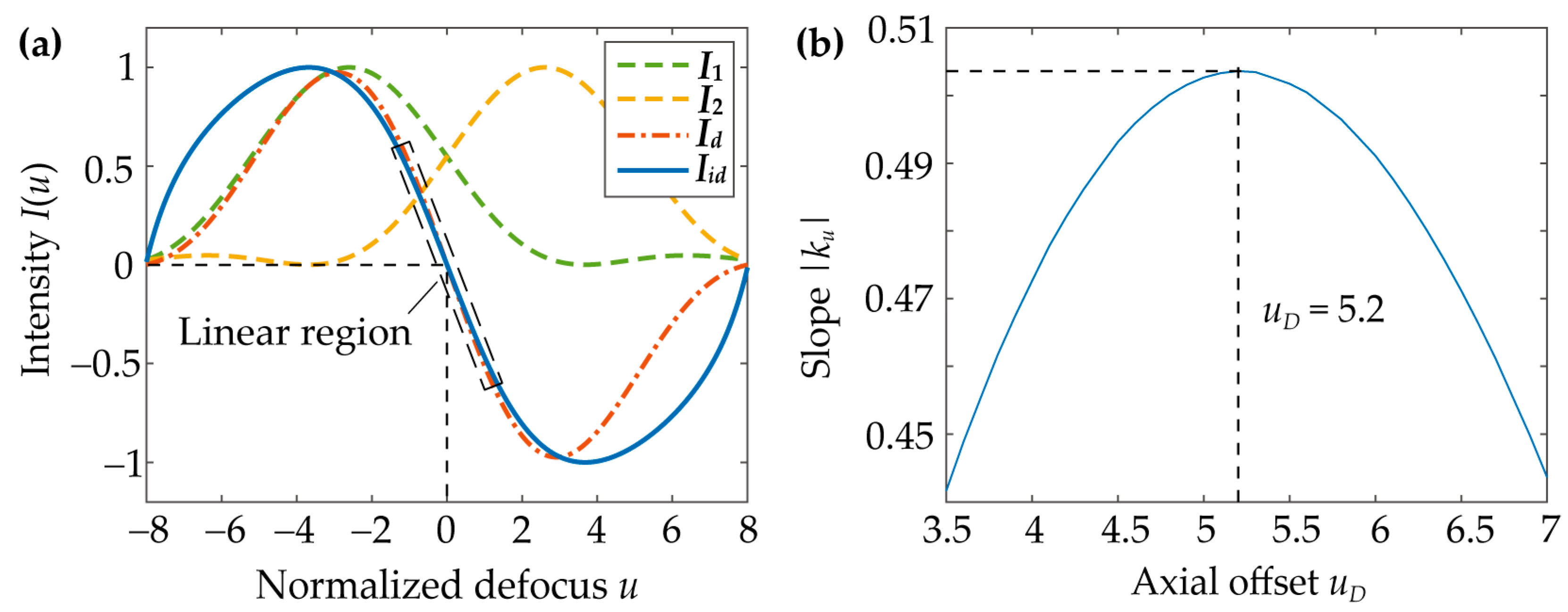
is a zero-order Bessel function. The normalized intensity response curves of
and
are shown in
Figure 2a, corresponding to the green and yellow dashed lines, respectively. They retain nearly the same shape as the conventional confocal axial response curve, but equal and opposite phase shifts are introduced into the curves due to the symmetrical axial displacements of the two pinholes from the imaging focal planes. The differential intensity response signal of BADCM can be expressed as
which is shown as the red dash-dotted curve in
Figure 2a. The relationship between the differential intensity signals and the normalized defocus values is approximately linear in the segment enclosed by the black dotted rectangle, which is considered the linear response region. Through linearly fitting the differential intensity response curve in the linear region, the amount of defocus can be uniquely determined by analyzing the obtained differential intensity signal. Furthermore, the null point of
curve strictly corresponds to the axial position of the focus point of the objective lens, providing the absolute measurement zero of the defocus. The sign of the differential intensity signal provides a good indication of the displacement direction of the substrate.
The intensity response signals are obtained from two detectors as the substrate departs from the focal plane of the objective lens along the optical axis and the defocus amount. The defocus amount can be calculated as
where
denotes the detected variation of differential intensity signal and
is the slope of differential axial response curve
in the linear response region. It can be seen from the formula that the larger the slope
, the higher the defocus detection sensitivity. The slope
at the zero point is much larger than that of conventional CM, thereby showing that BADCM holds the capability to detect defocus with higher precision near the system focus. The axial offset of the pinhole exerts a significant influence on the slope
and the slope
as a function of the normalized optical axial offset distance
is shown in
Figure 2b. The slope
varies as the distance
increases and reaches its maximum value while
. Therefore, the offset of the pinhole in the optical axis should be set to the corresponding optimum value to maximize the detection sensitivity of defocusing. In addition, the detection sensitivity can also be improved by increasing the effective numerical aperture of the objective lens, as shown in Equation (6). The adoption of a high NA objective lens in TPL for high-precision manufacturing just contributes to the high sensitivity of detecting the axial movement of the substrate.
The difference between the signals from two detectors can suppress the additive mode noise introduced in the common optical path in theory, compared with the conventional CM using a single detection. However, multiplicative mode noise in the optical path, mainly caused by fluctuations in the power of the light source and variation of refractive index at the substrate interface in actual measurement, also has an impact on the intensity response signals from the detectors and cannot be inhibited effectively by only utilizing differential subtraction. To reduce the measurement error, the post-processing can be improved [
23], and the improved intensity response signal of IDCM can be further expressed as
where
r is the coefficient of multiplicative mode noise, mainly representing the coefficient of fluctuations of laser power or refractive index at the substrate surface, and
is the additive noise. Generally,
. It can be seen from the formula that the additive noise and multiplicative disturbance in the intensity response signal of IDCM is obviously resolved. The resulting response signal is not affected by the instability of the light source intensity during defocus measurement, which improves the anti-noise performance of the autofocus system. The insensitivity to the substrate surface refractive index allows IDCM to be applied to a variety of substrates with different interface refractive indexes, such as silicon and silica, or substrates with a non-uniform surface refractive index. The axial intensity response curve of
is shown as the blue solid curve in
Figure 2a. It also has a monotonic and linear response range near the system focus and provides the absolute measurement zero point and the great discrimination ability of defocus direction. The slope of the
curve in the linear response range continues to increase as the axial offset value of the pinhole increases [
23], but the linear response range decreases at the same time. To balance the effective defocus measurement range and sensitivity, the pinhole axial offset can be determined as the optimum value for the maximum slope of the differential response curve
.
Based on the principle of IDCM, the defocus during manufacturing can be measured and compensated for as follows. Firstly, as a basis for defocus measurement, the axial intensity response curve of IDCM is calibrated by axially scanning the substrate with the PZT in the presence of photoresist, and the corresponding relationship between the intensity response signals and the displacement distances z is obtained. The slope of the response curve in the linear region is then solved using linear fitting. Next, the intensity response signals are obtained periodically during production, and the defocus amounts can be calculated as , where is the variation of the intensity response signals of IDCM. In actual measurement, the linearity of the intensity response curve in the working range may be unsatisfactory due to aberrations in the optical system, but it remains monotonous. To reduce the fitting error, a polynomial fitting could be employed to describe the functional relationship between the intensity response signals and the axial positions of the substrate. Finally, the PZT is moved with a distance of to perform a high-precision defocus compensation until the amount of defocus reaches the threshold set according to the focusing accuracy requirement. The coefficient -p is used to adjust the distance of movement of the substrate to reduce overshoot.
3. Results and Discussions
To verify the effectiveness of the proposed autofocus method for TPL pattern printing, an experimental system was constructed based on the schematic shown in
Figure 1. In the autofocus system, the continuous wave laser (FTEC2635-008SF0, Blue Sky, Milpitas, CA, USA) with a wavelength of 635 nm was employed, which hardly affected the photoresist. The dichroic mirror (ZT635dcrb, Chroma, VT, USA) could reflect the 635 nm light beam with 96% reflectivity and allowed the excitation light of the TPL to pass through. The microscope objective lens (CFI Plan Apo 100X Oil, Nikon, Tokyo, Japan) with NA of 1.45 was used to focus the incident beam and collect the reflected light. The PZT stage (P-563.3CD, PI, Karsruhe, Germany) could control the substrate to move along the
X,
Y, and
Z directions with an accuracy of about 1 nm. The size of the pinholes was 50
, and two PMTs with typical noise of 43 nV (R928, Hamamatsu, Shizuoka Prefecture, Japan) were used to collect the reflected intensity signals. A microscope cover glass with a size of 22 mm × 22 mm, a thickness of 170
, and a refractive index of about 1.52 was used as the substrate (0107052, Deckgläser, Karsruhe, Germany). It was cleaned first, and then the photoresist was dropped on it.
The optical path of the TPL was shown as a green light beam in
Figure 1. The femtosecond pulsed laser (Fs Laser, Chameleon Ultra II, Coherent, Santa Clara, CA, USA) generated a pulsed beam with a wavelength of 532 nm and a pulse width of 140 fs for two-photon production. Modulated by an acoustic optical modulator (AOM, AOMO 3080-120, Gooch & Housego, Ilminster, UK) and a galvanometer mirror (GM) device, the excitation beam passes through a scanning lens (SL) and a tube lens (TL), and is then focused by the objective lens onto the interface of the substrate and photoresist. AOM is applied to control the switching state and intensity of the incident light to create specific print patterns and determine the line width of the structures. GM scans the focal point of the excitation beam in the XY plane by changing the beam deflection. The field of view is illuminated by a light-emitting diode (GCI-060402, 589nm, Daheng Optics, Beijing, China) to observe the fabricated structures.
3.1. Performance of Autofocus Method
In the TPL system with a high NA objective lens, the shallow DOF requires a high defocus detection sensitivity of the autofocus system to detect the tiny amount of defocus. For this reason, a test of the detection sensitivity of the experimental system was performed. The PZT controlled the substrate to move along the optical axis in steps of 5 nm, and the positions of the substrate were measured 100 times after each step. To suppress the high-frequency noise, each individual response signal was obtained by averaging 1000 data collected by a data acquisition card (DAQ) at a sampling frequency of 1M Hz, as shown in
Figure 3. One hundred axial positions of the substrate relative to the focal plane of the objective lens were measured at each position of the substrate in 0.1 s. The results indicate that the defocus detection system can discriminate the 5 nm change in axial distance. Therefore, the detection sensitivity can reach 5 nm. The fluctuation of the measured distances could mainly result from the residual noise in the two detection optical paths and the detectors as well as the instability of the PZT.
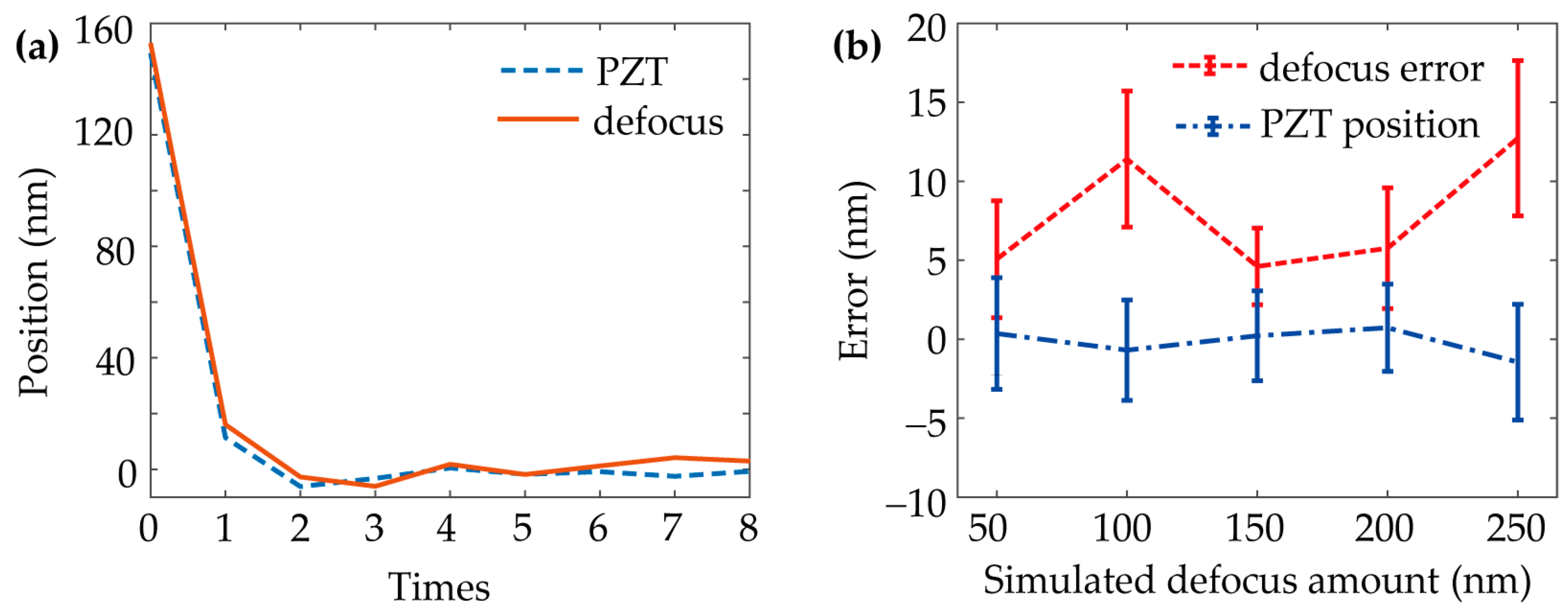
A high-precision focal plane detection system not only needs high detection sensitivity, but it also needs high repetitive measurement and focusing accuracy to measure the defocus amount and move the substrate back to the focal plane. Therefore, a compensation experiment was carried out. After moving the PZT controlled substrate a certain distance, the amounts of defocus were measured and compensated, as shown in
Figure 4a. In the figure, the measured defocus amounts and the recorded positions of the PZT nearly overlap with the simulated defocus amount of 150 nm, indicating that the measured defocus amounts can describe the actual motion of the substrate well. To obtain the repetitive measurement accuracy, the compensation experiment was carried out for different defocus amounts, and 10 times for each defocus amount. The differences between the detected defocus amounts and the PZT positions were calculated just after the substrate defocused, then named as defocus error (as shown in
Figure 4b). The results of defocus error in different simulated defocus amounts indicate that the repetitive measurement accuracy was less than 15 nm, which is mainly affected by the fitting error and system residual noise. In
Figure 4b, the blue dash-dotted line denotes the PZT positions after compensations at each simulated defocus amount. The standard deviations are less than 5 nm, preliminarily illustrating that the focusing accuracy can reach 5 nm, which is consistent with the detection sensitivity.
To further evaluate the long-term focusing performance of the autofocus system, experiments of defocus detection and compensation in a certain time were conducted. In
Figure 5a, the detected defocus amounts were measured in 15 min, and the compensations were performed every 3 min via PZT. The detected defocus amount changed significantly within 3 min and returned to 0 at every three-minute time point. This implied that the substrate drifted relative to the objective lens when the PZT retained stable and was pulled back to the focal plane while the autofocus was turned on, proving the effectiveness of defocus compensation.
Figure 5b shows the defocus amounts measured with autofocus on and off. The substrate moved about 500 nm relative to the objective lens in 20 min without autofocus. However, when the autofocus system was always in operation, the mean and standard deviation of the defocus amounts were 0.02 nm and 5.37 nm, respectively, indicating that the variation of the substrate positions relative to the focal plane of the system could be maintained within 5.37 nm. The results prove again that the focusing accuracy can reach about 5 nm, which is limited by the detection sensitivity and the stability of PZT.
3.2. TPL Fabrication with Autofocus System
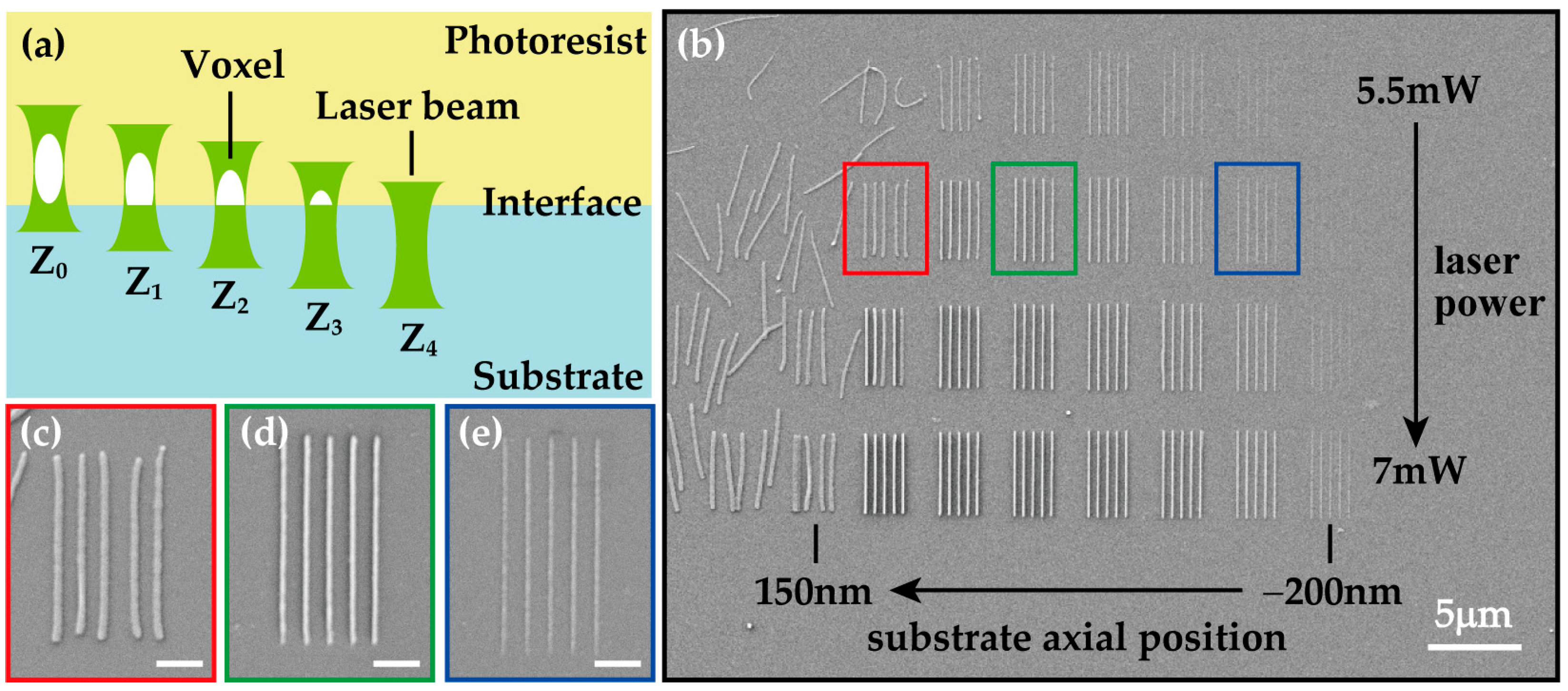
In TPL fabrication, the shape and size of polymerized voxels depend on the penetration depth of the laser focal point, which is affected by the defocus of the substrate. To study the effect of the defocus on the fabricated structures, a grating array was produced with the change of axial positions of the substrate and excitation laser power at the pupil of the objective lens. The schematic diagram is shown in
Figure 6a. The penetration depth of the laser focal point decreases with the approach of the substrate and the objective lens, and the lateral and axial sizes of the polymerized voxels are reduced at the same time.
When the focal spot is located at the
or
position, the voxels are mainly polymerized in the photoresist and adhere poorly to the interface. Hence the strength and adhesion of the produced structures will be reduced. When the focal spot is located at
or
position, the size of the polymerized voxel is small and the intensity of the excitation light cannot be used efficiently. Only when the laser focal spot is at
position (i.e., the focal plane) can the structures be stably machined on the substrate.
Figure 6b shows the scanning electron microscopy (SEM) image of the grating array. A group of grating contained five lines with a length of 5
and a spacing of 0.5
, and the spacing between the groups was 2
. The axial positions of the substrate corresponding to the printed grating groups increased in steps of 50 nm from right to left in the figure. The excitation laser power also increased at the interval of 0.5 mW from top to bottom. It could be clearly seen from
Figure 6c that, when the interface was 100 nm away from the focal plane of the objective lens, the manufactured lines were curved and the spacing between adjacent lines is uneven. This was attributed to the fact that the focal spot was at
position in the schematic diagram, the lines shifted due to the low adhesion on the interface. The processing quality of the lines was satisfactory while the interface just coincided with the focal plane, shown in
Figure 6d. When the interface was close to the focal plane at −150 nm, the lines were narrowed shown in
Figure 6e, which was unable to meet the design requirement. The results illustrated that defocus would exert a negative impact on the fabrication of the structures, which became more pronounced when the light power decreased. Thus, it must be measured and compensated by a high-precision autofocus system to ensure the quality of the structures.
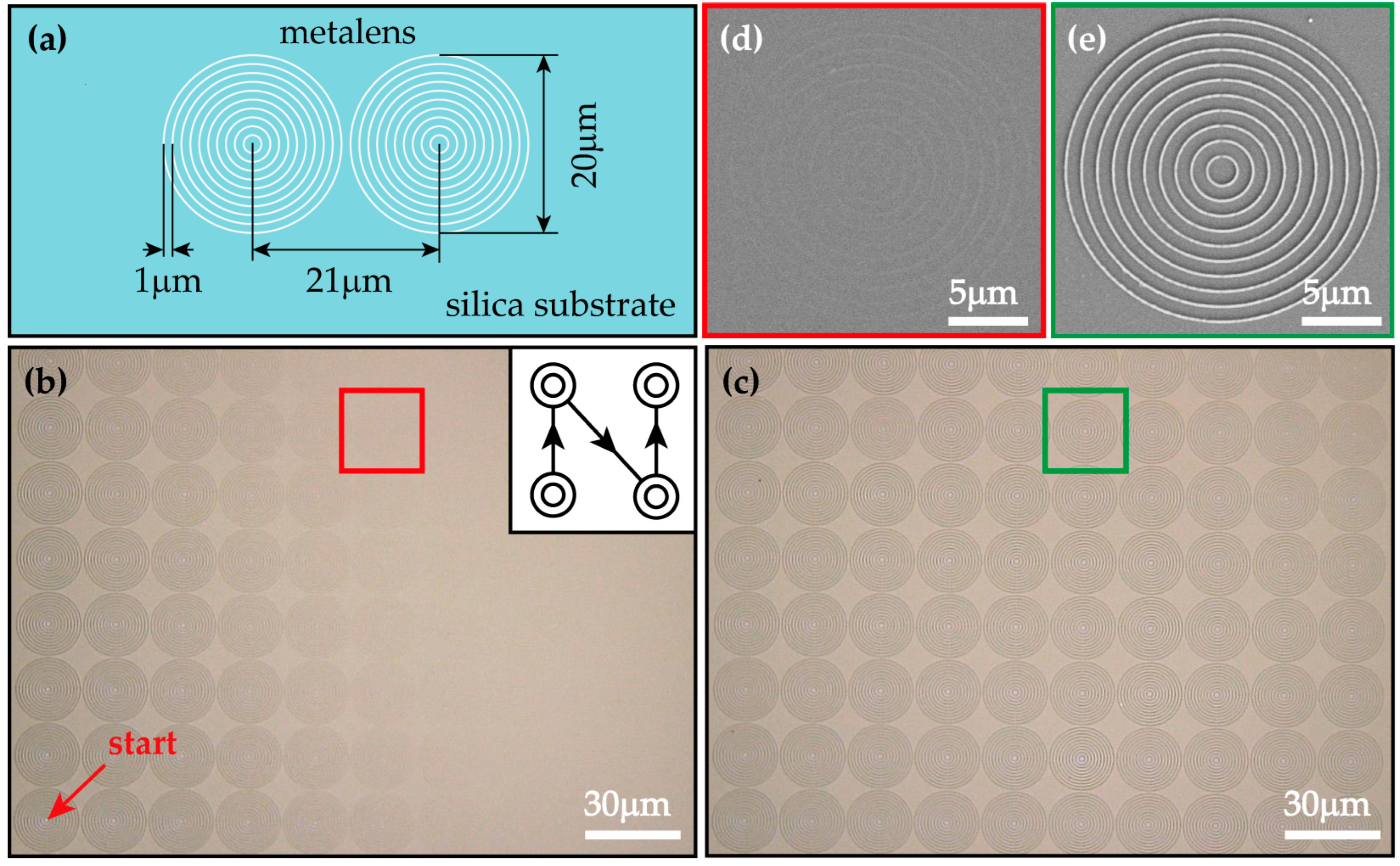
To verify the effectiveness of the autofocus system based on IDCM in actual fabrication, an 8 × 10 metalens array [
29] was fabricated on the coverslip. The PZT controlled the substrate to move in the
X-
Y plane to change the position of each fabricated metalens. The autofocus was carried out at each position of the metalens before the laser exposure. Each metalens was composed of concentric rings with a radius interval of 1
and a maximum diameter of 20
, shown in
Figure 7a. And the distance between adjacent lenses was 21
.
Figure 7b,c illustrate the results of optical microscopy analysis of the fabricated structures with the autofocus off and on, respectively. In
Figure 7b, the metalens array was printed starting from the lower left corner of the image (indicated by a red arrow) and along the route shown in the inserted figure. However, the latter half of the array could hardly be printed due to the gradual substrate drift without the autofocus system. The substrate tilt also led to the processing interface deviation from the focal plane. As a result, both temporal and spatial defocus occurred, degrading the fabrication quality of the structures. In contrast,
Figure 7c shows the fabrication of the metalens array when the autofocus was turned on. The defocus amounts at the positions of the structures were measured and compensated with high accuracy. This helped stabilize the substrate on the focal plane during the 18-min production, contributing to the excellent fabrication quality of all metalens in the field of view. The SEM images of the enclosed metalenses in
Figure 7b,c (
Figure 7d,e, respectively) demonstrate the crucial role of a high-precision autofocus system in ensuring high-quality microstructure manufacturing. The decrease in structure size in
Figure 7d may have resulted from the reduction of the penetration depth of the laser focal spot in the photoresist, which is caused by the defocus of the substrate close to the objective lens.
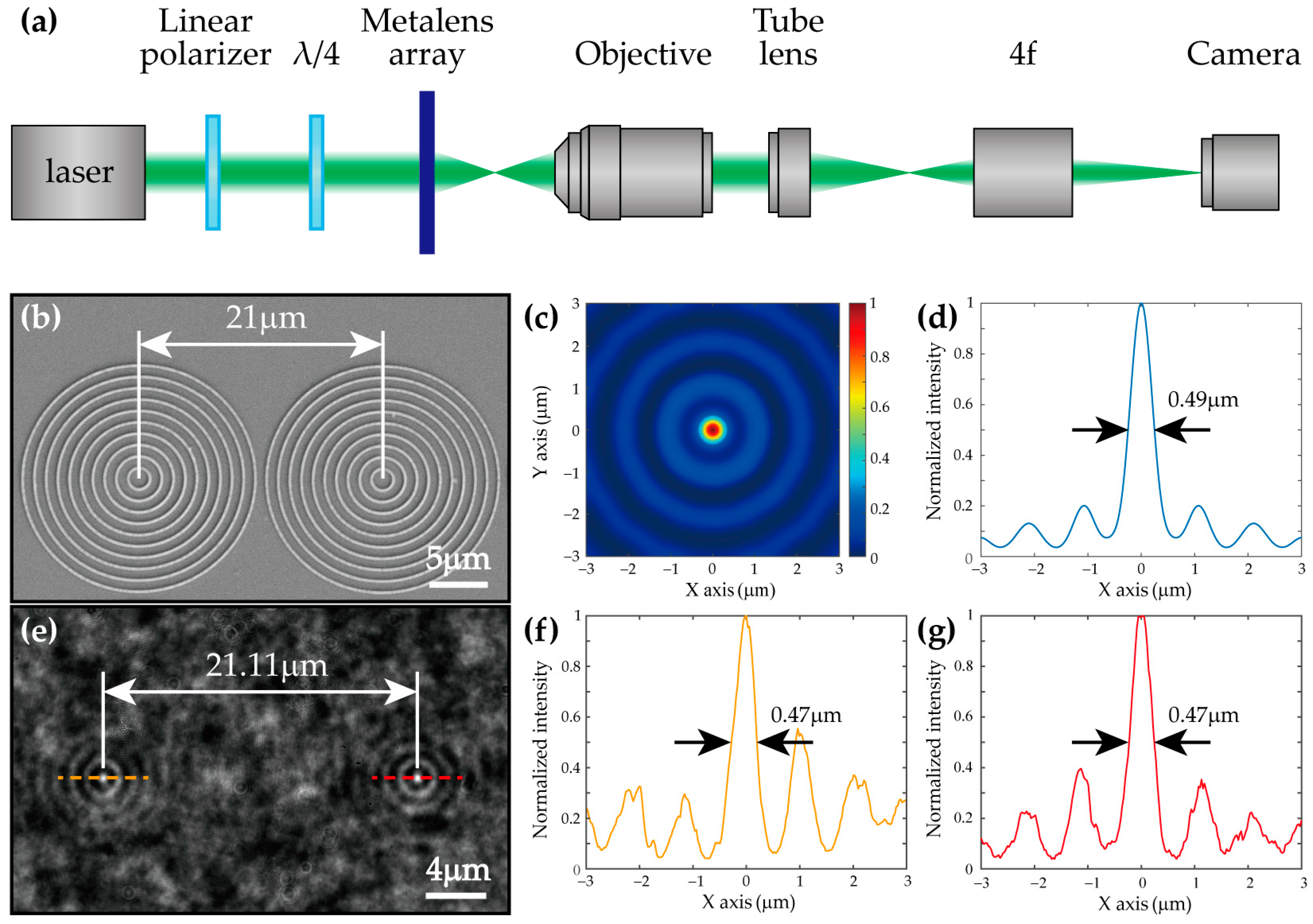
To characterize the performance of the fabricated metalenses, the intensity profiles at the focal plane were measured in an optical system shown in
Figure 8a. The sample was illuminated by a 520 nm laser beam. An objective lens (50×, NA = 0.95), a tube lens, and a 4f system (2.5×) were used to image the focal spot on a camera. The simulation of the structure shown in
Figure 8b was set up and performed using Finite difference time domain (FDTD). An x-polarized plane-wave source with its phase set to 0 and a y-polarized plane-wave source with its phase set to 90° were used to generate a circularly polarized incident beam, with a wavelength of 520 nm. The intensity profile of the focal spot was shown in
Figure 8c.
Figure 8d depicts the horizontal cut of the focal spot, with the full width at half maximum (FWHM) of 0.49
and the spacing of 1
between the side lobes. Then, the focusing performance of the structure was shown in
Figure 8e. It could be seen that the intensity profile of each focal spot had a similar shape to the simulation result in
Figure 8c, and the distance between the two focal spots was measured as 21.11
after the calibration of the imaging system, which is very close to the designed distance 21
. The bright and irregular background could mainly due to the noise in the optical system and camera. Furthermore, the horizontal cuts corresponding to the orange and red dashed lines were shown in
Figure 8f,g. The FWHMs of both cuts were measured as 0.47
, and the distance between the side lobes was also around 1
, consistent with the simulation results. The consistency between the actual characterization and simulation results illustrated that the fabricated metalens met the design requirements well and evidenced the excellent performance of the autofocus system.


