Review

Long-Wavelength VCSELs: Status and Prospects

1
Institute of Advanced Data Transfer Systems, ITMO University, Saint Petersburg 197101, Russia
2
Ioffe Institute, Laboratory of Physics of Semiconductor Heterostructures, Saint Petersburg 194021, Russia
3
Alferov University, Saint Petersburg 194021, Russia
4
Connector Optics LLC, Saint Petersburg 194292, Russia
5
Bimberg Chinese-German Center for Green Photonics, Changchun Institute of Optics, Fine Mechanics and Physics (CIOMP), Chinese Academy of Sciences (CAS), Changchun 130033, China
6
Center of Nanophotonics, Institute of Solid State Physics, Technische Universität Berlin, 10623 Berlin, Germany
*
Author to whom correspondence should be addressed.
Photonics 2023, 10(3), 268; https://doi.org/10.3390/photonics10030268
Submission received: 31 January 2023 / Revised: 24 February 2023 / Accepted: 27 February 2023 / Published: 3 March 2023

Abstract

:
Single-mode long-wavelength (LW) vertical-cavity surface-emitting lasers (VCSELs) present an inexpensive alternative to DFB-lasers for data communication in next-generation giga data centers, where optical links with large transmission distances are required. Narrow wavelength-division multiplexing systems demand large bit rates and single longitudinal and transverse modes. Spatial division multiplexing transmission through multicore fibers using LW VCSELs is enabling still larger-scale data center networks. This review discusses the requirements for achieving high-speed modulation, as well as the state-of-the-art. The hybrid short-cavity concept allows for the realization of f3dB frequencies of 17 GHz and 22 GHz for 1300 nm and 1550 nm range VCSELs, respectively. Wafer-fusion (WF) concepts allow the realization of long-time reliable LW VCSELs with a record single-mode output power of more than 6 mW, 13 GHz 3 dB cut-off frequency, and data rates of 37 Gbit/s for non-return-to-zero (NRZ) modulation at 1550 nm.

1. Introduction

According to Yole Intelligence’s annual ‘VCSEL—Market and Technology Trends 2022 report [1], the datacom sector of the vertical-cavity surface-emitting lasers (VCSELs) market is growing at 22.2%/year, regaining the lead from the mobile and consumer sector, which are growing at 15.7%/year.
The use of long-wavelength (1300–1550 nm) single-mode (SM) VCSELs makes it possible to reduce the modal and chromatic dispersion in an optical link and, as a result, to extend its reach. Moreover, spatial division multiplexing (SDM) transmission by multicore fibers using long-wavelength (LW or short-wavelength infrared, SWIR) VCSELs are enabling many larger-scale data center networks [2] than presently possible. A review of data communication and telecommunication by LW VCSELs can be found in ref. [3]. 1550 nm SM VCSELs are promising not only for next-generation short-reach optical interconnects but also for SDM transceivers. In fact, the large output power and dynamic characteristics of 1550 nm VCSELs [4] demonstrate their potential for large distance transmission (e.g., 1 km), where high bit rate SM emission is a prerequisite for operating narrow wavelength-division multiplexing systems (e.g., for 5 km distance). Moreover, 1550 nm widely tunable micro-electro-mechanical system (MEMS) VCSELs are used for wavelength DM passive optical network (WDP-PON) systems [5] with VCSEL-based SFP+ modules and THz photomixing [6].
Due to the absence of mode-hopping effects in short cavities, where longitudinal-mode spacing is larger than the mirror stopband, 1950 nm range MEMS VCSELs can be applied for tunable diode laser absorption spectroscopy (TDLAS) [7]. LW VCSELs (1300–2300 nm) can also be used for gas sensing, including HF, H2O, NH3, CH4, HCl, H2S, CO2, CO, N2O, ethylene oxide, and combustibles [8,9].
1300 nm VCSELs are of particularly strong importance for hybrid integration with silicon photonics, providing integrated modulators and InP- and GaAs-based integrated photonic circuits [10,11,12,13]. Other emerging markets for 1300 nm VCSELs include eye-safe-based Laser Imaging Detection and Ranging (LiDARs) [14] and light sources for 5G (fifth generation) mobile and optical wireless applications [13]. High-power SM VCSELs operating uncooled up to large on-chip temperatures are demanded. Modulation bandwidths >5 GHz are preferable for time-of-flight applications to realize short raise and fall times <1 ns. Novel proximity sensors may be based on 1380 nm VCSELs, enabling integration with organic light-emitting diodes (OLEDs). A shift of the VCSEL emission wavelength to 1380 nm will enable using these VCSELs behind OLED displays, replacing the laser diodes that are being currently used, e.g., in the proximity sensor under the display in the iPhone 14 Pro© [1]. Therefore, the first large-scale application of LW VCSELs might be proximity sensors for smartphones. TRUMPF Photonic Components GmbH aims to bring the first SWIR VCSEL products to the high-volume market in 2025 [15,16].
In this paper, we present a review of the current status of LW VCSEL development and the relevant technologies. In Section 2, the various distributed Bragg reflectors (DBRs) that are used for the fabrication of 1300–1550 nm spectral range VCSELs are compared. In Section 3, we focus on the approaches to realize strong current confinement. The present status of monolithic LW VCSELs grown on GaAs and InP substrates is presented in Section 4 and Section 5, respectively. Hybrid VCSELs with active regions grown on InP wafers will be discussed in Section 6. Approaches for the fabrication of LW VCSEL by wafer fusion techniques are described in Section 7.

2. Distributed Bragg Reflectors for the 1300–1550 nm Spectral Range

Monolithic DBRs lattice-matched to InP based on InGaAsP/InP [17,18], AlInGaAs/AlInAs [19], or AlGaInAs/InP [20] heterostructures suffer from very low refractive index contrast (∆n). At 1550 nm, the refractive index contrast is ~0.3. At 1300 nm, ∆n is only ~0.2 [21], since the band gap of the layers must be increased to avoid absorption. Larger maximum ∆n values are provided by AlAs/GaAs pairs (∆n ~ 0.5) and AlGaAsSb/AlAsSb pairs (∆n ~ 0.49). Growth of, e.g., a bottom mirror with 99.9% reflectivity requires epitaxy of 63 pairs of InAlGaAs/InP (∆n ~ 0.19) [21]. DBRs on GaAs substrates provide the same reflectivity with only 23 AlAs/GaAs pairs. AlAs/GaAs can also be used for the 1550 nm spectral range. AlGaAsSb-based DBRs combined with aperture formation based on an air gap fabricated by selective etching of an imbedded tunnel junction (TJ) allowed the development of LW VCSELs [22]. A disadvantage of this approach is the low thermal conductivity of such mirrors, which leads to early turn-over of the output power with increasing current and their predisposition to oxidation.
An alternative approach for mirrors with high reflectivity for LW VCSELs is DBRs based on an InP/Air gap combination [21]. The refractive index contrast in such DBRs is 2.2, and only three pairs of quarter-wavelength layers are required to reach 99.9% reflectivity. However, the thermal and current conductivities of InP/Air pairs of such mirrors are extremely low. Only configurations with double intra-cavity contacts and a thick heat dissipation layer based on InP were reported until now. In addition, a design with air gaps is quite fragile. Since the thermal resistance of DBRs is directly proportional to the number of pairs in the DBR and also depends on the composition of the layers [23], dielectric DBRs are also advantageous as compared to DBRs based on AlAs/GaAs while achieving the same mirror reflectivity. Hybrid DBRs combining several pairs of dielectric DBRs and a layer of gold enable a compromise from the point of view of minimizing the thermal resistance of LW VCSELs DBRs. The thermal conductivities of various materials have been studied, such as amorphous silica (a-Si), MgF2, CaF2, Al2O3, and ZnS [23] ranging from 6.83 WK−1m−1 (for ZnS [23]) to 2.4 WK−1m−1 (for a-Si [23]). Al2O3/a-Si pairs show the best thermal behavior, but ∆n is only 1.6 and high loss is typical. 2.5 pairs of CaF2/a-Si (∆n = 1.9) provide a thermal resistance of less than a third of the value of the corresponding epitaxial mirror (7.4 × 10³ K/W) [23,24]. 2.5 MgF/a-Si pairs (∆n = 1.9) enable reducing the thermal resistance down to 5.6 × 10³ K/W [25,26]. However, due to significant losses of a-Si at 1550 nm (400 cm−1 [23,25]), 2.5 pairs of CaF2/ZnS are used [2] to develop hybrid DBRs for 1550 nm VCSELs with 99.85% reflectivity. The thermal resistance here is only 6.8 × 10³ K/W. In general, before p-type contact fabrication, natural oxides are removed from the contact layer surface by wet etching in diluted hydrochloric acid (HCl) or ammonia (NH3). Moreover, the InP substrate can be removed by wet etching in HCl. Due to the solvent possibility of CaF2 in HCl and NH3 in further works, authors began using DBRs based on AlF3/ZnS for the development of 1550 nm VCSELs. AlF3/ZnS DBRs are compatible with the HCl cleaning process but have a lower ∆n (about 1.0) in relation to CaF2/ZnS [27]. The penetration depth in AlF3/ZnS DBR is about 300 nm [28]. The use of five AlF3/ZnS pairs provides a reflectivity of 99%. Here, the mirror thickness is about 2.4 µm, as compared to 7 µm for a semiconductor DBR based on 30 AlGaInAs/AlInAs pairs [29].
For wavelengths at or below 1300 nm, the number of CaF2/ZnS pairs is 3.5 [30], due to an ∆n of 0.85 [24]. For 1300 nm VCSELs DBRs based on AlF3/ZnS were also used [31], showing a larger difference in the refraction index (∆n = 0.95).
A completely novel approach to largely increases heat dissipation based on circumventing the mirrors for current injection and heat dissipation is reported by Tian et al. [32,33].
High-contrast gratings (HCG) might well be used in the future for the top DBRs [34,35,36,37,38,39,40,41]. Buried tunnel junction (BTJ) and/or proton implantation are used to provide current confinement for HCG at 1300–1550 nm VCSELs. The principal advantages of HCGs in a VCSEL include transverse mode control, fixed polarization, and reduced manufacturing cost (reduction of the epitaxial growth time) [42]. Lasing via fundamental mode allows one to realize high SM output power for HCG devices with large apertures. HCGs are promising to realize widely tunable VCSELs. A review by C. Chang-Hasnain in this volume reports in depth about HCG-based VCSELs. HCG provides an extraordinarily wide stopband [43]. More than 98.5% reflectivity in the 1120–1620 nm spectral range was demonstrated [44]. The additional advantage is wavelength scalability. By multiplying the dimensions of HCG (by 6.5), the reflection band center shifts from 1.55 μm to 10 μm [45]. HCG-VCSEL lasing wavelength can be tuned by the HCG period and duty cycle [43]. As a result, monolithic multi-wavelength VCSELs were realized [46]. The use of HCG as a movable mirror allows one to realize the tunable VCSELs with a wide tuning range as well as rapid tuning speed [35,47,48,49]. The detailed study of a systematic review of experimental and modeling results as well as fabrication tolerance can be found in ref. [43]. In both uniform and random-size HCGs, a very large fabrication tolerance in HCG-VCSELs is demonstrated [43]. The main drawback of near-infrared subwavelength HCG VCSELs is their modest dynamic performance in relation to VCSELs with semiconductor mirrors as well as the challenging processing related to electron-beam lithography usage [50].
On the other hand, the dynamic performance of SWIR HCG VCSELs is comparable (about 8 GHz modulation bandwidth for 1500 nm VCSELs [3,34,39]) with the same value for wafer-fused VCSELs but inferior to the superior modulation performance of hybrid LW VCSELs. MEMS-tunable 1550 nm VCSELs demonstrate the reliability of Telcordia GR468 [51].
A different type of DBR is based on MEMS. Using 11.5 SiOx/SiN pairs [6] allows one to realize 7 GHz [5] and 9 GHz [7] modulation bandwidth for 1500 nm VCSELs. The ∆n value for SiOx/SiN is about 0.47. Using SiOx/SiCz DBRs [52] allows one to increase the ∆n value to 1 [53]. As a result, the pair number can be decreased to 6.5 instead of 11.5 for reflectivity of >99.5%. Finally, the stop band width is 243 nm (at a reflectivity of >99.5%) and is about twice that of the SiOx/SiN pair. As a result, the small IR absorption of SiCz can be diminished due to the wider tuning range compared to SiOx/SiN-based MEMS DBRs.

3. Current Confinement and Tunnel Junctions

Current confinement in InP-based LW VCSELs can be achieved by selective lateral etching of AlInAs-based TJs (so-called air-gap aperture), which is part of the whole TJ [54]. The use of a TJ allows one to inject holes through an n-doped region, thereby reducing the series resistance and free carrier absorption. Further, the BTJ concept was used for current confinement in InP-based LW VCSELs. The active region is embedded here between n-InP and p-AlInAs for effective carrier confinement. Due to the poor electrical, thermal, and optical properties of AlInAs, it is necessary to reduce their thickness [3]. BTJs allow one to reduce the thickness of AlInAs to one-quarter of the emission wavelength and replace it with low-resistance n-InP, yielding the desired cavity length [3]. BTJ for short-cavity VCSELs was first developed by Prof. Amann’s group, whereas regrown tunnel junctions embedded in wafer-fused VCSELs were developed by Prof. Kapon’s group [55]. Below, we use BTJ denotation for both types of TJs.
The main idea of BTJs for LW VCSEL design is to use a laterally structured tunnel junction inside a p-type layer to:
-
convert most of the current confinement layers in the p-type region from p- to n-type to get lower electric resistance, reducing self-heating;
-
use ohmic contacts from two sides to n-type layers with low contact resistance;
-
reduce optical losses in n-type layers used at the former p-side of the laser;
-
use intra-cavity contacts with low resistance;
-
achieve effective lateral current confinement;
-
achieve strong lateral optical confinement [56].
The principal structure and electric circuit of BTJs are presented, e.g., in refs. [56,57]. To realize SM lasing, the topology of the overgrown surface relief and the etching depth of TJs should be considered. The lateral refractive index contrast is qualitatively determined by the height of overgrown TJ (∆L) [3]: ∆neff/neff = ∆L/L, where neff is the effective refractive index and L is a microcavity length. The BTJ consists here [3] of highly doped p- and n-type (InGaAl)As layers. The BTJ is located on the p-side of the diode. The side walls of the BTJ are formed by selective etching of the n+-InGaAs top layer and parts of the bottom p+ InAlGaAs layers, which contain only a few percent of aluminum [58]. The BTJ is overgrown by a moderately doped n-InP layer. Therefore, when a reverse bias is applied to the BTJ, the p+n+ junction demonstrates ohmic behavior and extremely low resistance due to tunneling. The BTJ is located in a node of the optical field aimed at eliminating free-carrier absorption in the heavily doped TJ layers. p+-InGaAlAs/n+–In(Al)GaAs TJ can be grown by molecular-beam epitaxy (MBE), chemical beam epitaxy [26,59], and metalorganic vapor-phase epitaxy (MOVPE) [56,60,61]. Using MBE involves an extra hydrogen cleaning procedure [62,63] based on the RF source in the chamber [64,65] to deoxidize the oxidized InGaAlAs surface before TJ regrowth. Growth of InAlGaAs-based BTJs is difficult in industrial MBE systems.
An alternative approach is using composite n++-InGaAs/p++-InGaAs/p++-InAlGaAs TJs [10,66,67]. A similar approach to using aluminum-free (n++-InGaAs/p++-InGaAs) TJs was previously presented in ref. [68]. In both cases, solid-source MBE regrowth, including the surface planarization effect, is absent [3,10,26,59,61,69] and shows strong index-guiding results as compared to MOVPE regrowth.
Additional attention is devoted to doping optimization of the overgrown InP layer at BTJ formation. As previously mentioned for hybrid VCSELs [27], the reduction of overgrown layer doping down to 1 × 1017 cm−3 allows one to increase the modulation bandwidth by 35% (from 6.7 to 9 GHz).
In addition to BTJs, current confinement can be achieved by ion implantation [34,70,71,72,73], leading to a planar device geometry. A disadvantage is the lack of inherent optical confinement [74].
To overcome the complicated implementation of high-level p-doping of InGaAs above 1 × 1019 cm−3 GaAs0.51Sb:C/Ga0.47InAs:Si BTJs were suggested to realize 1300 nm VCSELs [75] grown by MOCVD.
Alternatives to BTJs were considered. In contrast to the traditional AlGaAs layer’s high Al-composition in GaAs-based VCSELs, the use of InP-lattice-matched AlxIn1−xAs layers in InP-based VCSELs is complicated due to low oxidation speeds [3]. Selective oxidation of In0.78Al0.22As0.47P0.53 layers for the fabrication of 1550 nm oxide-confined VCSELs was shown in [76,77].
Results were also presented for developing current apertures by undercutting (selective chemical etching) the quantum wells (QWs) [21,22,78,79,80]. VCSELs with BTJ apertures, however, show better performance as compared to undercut QWs, implanted apertures, or selectively oxidized apertures.

4. Monolithically Grown VCSELs on GaAs Substrates in the 1300–1550 nm Spectral Range

The large refractive index contrasts of mirrors on GaAs substrates enable a reduction in the number of pairs in DBRs as compared to DBRs on InP substrates. Strained InGaAs, InGaP, InGaAsSb, GaAsSb, GaInNAs, and GaInNAsSb QWs are usually considered active regions for monolithic 1300-nm VCSELs grown on GaAs. Implementation of more long-wavelength VCSELs is possible by using GaInAsNSb/GaAs QWs.
In addition to QWs, quantum dots (QDs) based on InGaAs/AlGaAs were shown to serve well as active regions already two decades ago. InAs QDs and submonolayer QDs enable to control of the emission wavelength more flexibly and potentially reach a higher differential gain and lower threshold currents. The low density of QD arrays makes it necessary to stack rows of QDs to reach the required optical gain [81], which at the same time limited the output power and modulation bandwidth of 1280 nm spectral range devices to 0.3 mW and 2 GHz (the data transfer rate is 2.5 Gbit/s) at 20 °C, respectively [82]. Submonolayer QDs circumvented this problem, and 20 Gbit/s open eyes were demonstrated between 20 and 85 °C up to 1250 nm [83].
Using In0.42Ga0.58As QWs made is possible to demonstrate 10 Gb/s modulation at both 25 and 85 °C at 1280 nm emission wavelength, which is due to a large gain to cavity detuning, GCD (about 55 nm) (photoluminescence (PL) peak of In0.42Ga0.58As QWs is about 1220 nm) [84,85,86,87,88,89,90]. However, implementation of effective VCSELs beyond 1300 nm wavelength in the framework of this approach turned out to demand more work.
Using InAs0.44P0.56 strain-compensated QWs made it possible to implement multimode lasing at 1300 nm with an output power of about 1.9 mW [91]. Another approach was using GaAs0.665Sb0.335/GaAs QWs. Operation in continuous-wave (CW) mode was demonstrated at 1230 nm wavelength with 0.7 mA threshold current [92]. Later, the wavelength could be shifted to 1300 nm [93] by using GaAs0.63Sb0.36/GaAs QWs. CW operation at 70 °C has been demonstrated.
Multiple groups contributed to the development of VCSEL based on diluted nitrides, including industrial research departments (Infineon, Sandia/Cielo, JDSU/Picolight, Alight Technologies, Philips U-L-M Photonics, IQE etc.) [94,95,96]. Devices in the 1300 nm spectral range based on GaInNAs QW with 10 Gbit/s operating speed and more than 1.2 mW output power at 20 °C were demonstrated in Ref. [97]. The use of TJ and microcavity geometry with intra-cavity contacts enabled not just an increase in the modulation bandwidth up to 9.8 GHz at 20 °C but also an increase in the output power to 4.2 mW [98]. Several groups demonstrated data transfer rates of 10 Gbit/s [94,97,98,99,100,101]. However, the growth of GaInNAs QWs is associated with the decomposition of quaternary alloys into microscopic InGaN and InGaAs regions (phase segregation) and the formation of immiscibility regions, which requires more detailed research of the epitaxial growth of GaInNAs QWs. Moreover, the incorporation of N results in an increase in strain and the number of radiation defects. As a result, for long-term laser reliability, the nitrogen concentration in the QW should not exceed 1% for indium concentration larger than 30% [99], which limits the maximum VCSEL wavelength to the 1270–1280 nm range.
A partial solution of the phase segregation is associated with the use of Sb, which makes it possible to increase the critical thickness limit associated with the transition to 3D growth and maintain the high crystalline quality of the growing GaInNAsSb material [102]. Recently, the possibility of implementing devices with a 1300 nm emission wavelength and a maximum small-signal modulation bandwidth of 10.5 GHz has been shown [13,103]. The structure used was based on GaInNAsSb QWs and doped DBRs based on pairs of AlGaAs/GaAs. The current aperture was formed by lateral oxidation. The maximum data transfer rate amounted to 12 Gbit/s [13] for an output power of 0.6 mW.
The first VCSEL based on GaInAsNSb QWs with electric injection operating beyond the 1310 nm spectral range was presented in 2003 [104,105]. The device design consisted of a bottom DBR based on 29 AlGaAs/GaAs pairs, an active region based on GaInNAsSb/GaNAs QW, and a top DBR based on 24 p-doped AlGaAs/GaAs pairs. A VCSEL with a 1460 nm emission wavelength operated in pulse mode only when cooled to −10 °C. In 2006, an extension of GaInAsNSb-based VCSEL spectral range to a still longer wavelength was achieved when cooled to −48 °C [106]. In 2009, a monolithic GaInNAsSb-based VCSEL was demonstrated, which operated in pulse mode at 1530 nm wavelength at room temperature in CW mode, but the output power was less than 1 µW [107]. In 2019, GaInNAsSb-based VCSELs with an 8 µm aperture operated up to 4.3 GHz at a 3.9 mA threshold current. The output power again did not exceed 0.3 mW at room temperature in CW mode, and the maximum emission wavelength was 1490 nm [108]. Note that the growth of Sb-containing QWs is associated with additional technological difficulties due to the volatility of Sb.
An alternative approach is using layers of GaAsN/InAs superlattices [109], which makes it possible to minimize the effect of nitrogen diffusion from QWs [110]. The presence of the mini bands, being both in the QW region and in the barrier region, enables a significant increase in the overlap factor and, therefore, a significant increase in the modal gain as compared to QW-based active regions.

5. Monolithically Grown VCSELs on InP Substrates for the 1300–1550 nm Spectral Range

Monolithic VCSELs in the 1300–1550 nm spectral range fabricated on InP substrates are currently produced by the South Korean company RayCan [111] and the US company Bandwidth 10 [112].
RayCan developed 1550 nm VCSELs based on InAlGaAs/InP in a single epitaxial process with carrier injection via n-type intra-cavity contact layers (ICCL) and n-InP/p+-InAlAs/n-InP TJs [78]. The structures consist of a bottom (output) undoped DBR based on 28 InAlGaAs/InAlAs pairs, a bottom 2λ ICCL n-type layer, a 0.5λ cavity with an InAlGaAs QW-based active region, placed in the antinode of the optical wave, an n-InP/p+-InAlAs/n-InP TJ, a top 2λ n-type ICCL, and a top undoped DBR based on 38 InAlGaAs/InAlAs pairs.
Epitaxial structures are grown by MOVPE. For the formation of current and optical confinement, an air-gap aperture is used, obtained by selective lateral etching of optical cavity layers between ICCLs. To maximize the reflectivity and thermal conductivity of the top mirror, a bottom-emitted vertical cavity structure (emission output downwards via an InP substrate) is combined with a hybrid metal-semiconductor mirror in the form of a top DBR covered by a gold layer through a phase-matching layer. This approach is also used by B.S. Yoo’s group (Electronics and Telecommunications Research Institute, Republic of Korea). A cross-section of such a VCSEL is presented in refs. [78,113].
These VCSELs demonstrate single-mode lasing with more than 40 dB side mode suppression, 2.5 mA threshold current, and 1.6 mW maximum output power at room temperature. The laser’s series resistance amounted to 150 Ohm. A temperature increase to 70 °C leads to a threshold current increase to 4.2 mA, a decrease of the slope efficiency, and output power to 0.5 mW. As a result, the f3dB cut-off frequency does not exceed 4–5 GHz [114]. Error-free (bit error rate, BER < 10−12) data rates of 2.5 Gbit/s for up to 30 km optical fiber length were demonstrated [78]. In ref. [115], results of degradation studies of monolithic 1550 nm spectral range VCSELs produced by the RayCan are presented, using high-temperature tests; extrapolation of the results shows VCSEL life times of 2 × 10⁷ h. The development of prototype monolithic VCSELs for the 1550 nm spectral range up to 10 Gbit/s was recently announced [116]. For single-mode VCSELs, the threshold current is 2 to 3 mA, and the output power is 1 mW. For multi-mode VCSELs, the threshold current is 3 to 4 mA, and the output power is about 2 mW.
A research group from the University of California, Berkeley, and the US company Bandwidth 10 [112] also use a monolithic approach to make 1550 nm spectral range VCSELs. HCGs are used for the top output mirror [34,70,71]. The epitaxial structures consist of a bottom DBR with 40–55 pairs, an active region based on GaAlInAs QWs, a p-type cladding layer, TJ, a sacrificial layer, a layer to provide the HCG, and a top contact layer. The current aperture is provided by proton implantation. The aperture diameter depends on the design and varies in the range of 8 to 20 µm. HCGs are developed by electron-beam lithography and anisotropic vertical etching techniques. In CW mode, such VCSELs demonstrated output powers of 2.4 mW at 15 °C and 0.5 mW at 85 °C. HCGs provide the opportunity to implement single-mode laser operation with large diameters of the aperture, up to 12 µm. The maximum frequency of small-signal modulation is 7.8 GHz at a 2.5 threshold current. If a microelectromechanical actuator is added to the HCG, one can modify the wavelength in the 1540–1565 nm range while keeping the single-mode operation mode.
Bandwidth 10 is currently implemented in industrial production of VCSELs at 1300 nm and 1550 nm in TO-cans and TOSA-packaged versions, demonstrating rates of 10 Gbit/s at 1 mW output power into an optic fiber. Moreover, the tunable SFP+ modules operate across a 14+ nm tuning range at 10 Gbit/s [51]. LiDAR systems based on swept VCSEL were also demonstrated [36].

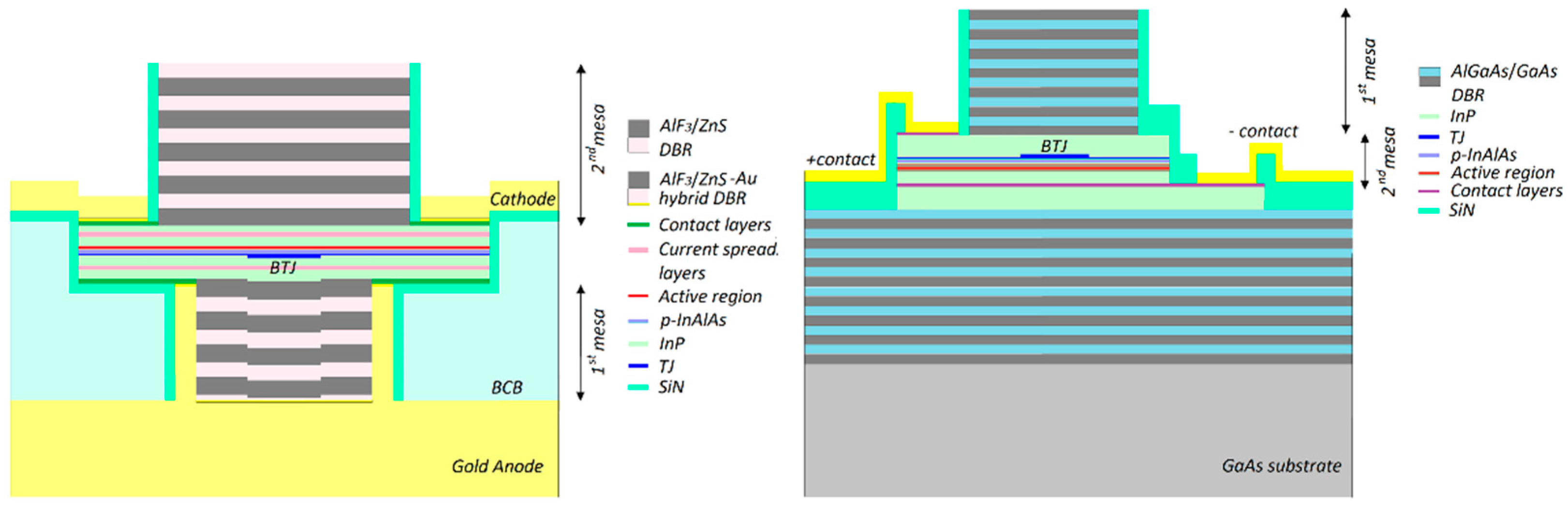
6. VCSELs with Hybrid (Metal-Dielectric) Distributed Bragg Reflectors

To increase the temperature stability of the output characteristics of 1550 nm VCSELs, the research group of the late Prof. M.-C. Amann (Walter Schottky Institute, Technical University Munich, München, Germany) proposed a hybrid technology for device fabrication, where a hybrid metal-dielectric mirror is used as a bottom mirror and the BTJ concept is applied [117]. A hybrid metal-dielectric mirror is a dielectric DBR covered by a thick layer of gold (about 50–60 µm [27,56]), which acts as a heat sink and provides mechanical stability since the InP substrate is fully etched away. Despite the lower thermal conductivity of dielectrics, the total thermal conductivity of a hybrid metal-dielectric mirror turns out to be significantly higher as compared to InAlGaAs/InAlAs DBRs. Lateral heat dissipation from the active region to the gold heat sink through InP ICCL also contributes to efficient heat removal. A schematic view of a hybrid VCSEL device is shown in Figure 1 (left panel).
The use of the BTJ concept enables not only effective current confinement but also optical confinement, similar to oxide-confined current apertures. Moreover, it enables reducing the series resistance and operating voltage, thus reducing the heat generation of the device. The laser structure consists of a cavity with an active region based on 7 InAlGaAs QWs, 6 nm thick, limited below by a bottom hybrid metal-dielectric mirror based on CaF2/ZnS and above by a top (output) doped DBR based on 32 n-type InAlGaAs/InAlAs pairs. Carrier injection is carried out via the n+/p+-InGa(Al)As TJ and top n-InP ICCL. The growth was performed by MBE. 1550 nm VCSELs with 5 µm TJ demonstrated single-mode lasing with more than 40 dB side mode suppression ratio, 1.5 mA threshold current, and 2.5 mW maximum output power at room temperature [118]. The series resistance depends on the pump current and varies in the 40–50 Ohm range. Due to the large mismatch between the gain spectrum and the resonance wavelength, a temperature increase leads to the non-linear behavior of the threshold current. As the pump current increases, the modulation bandwidth reaches 10 GHz at 3 mA and saturates at 12 GHz and 10 GHz at 25 °C and 85 °C, respectively [119]. Error-free data transfer (BER < 10−12) at 25 Gbit/s for up to 30 km of optical fiber length at 25 °C [118] and at 12.5 Gbit/s up to 85 °C [117,119] was demonstrated.
A short cavity with both dielectric mirrors, where carrier injection takes place through intra-cavity contacts layers [120] was recently demonstrated to further increase the data rate of VCSELs based on the hybrid concept. The main difference is the formation of output dielectric mirrors. By replacing the output doped n-type InAlGaAs/InAlAs-based DBR with AlF3/ZnS-based dielectric DBR [28] (cf. Figure 1, left), the effective cavity length was reduced, the modulation bandwidth was increased to 18 GHz, and the data rate was increased to 35 Gbit/s at 20 °C and 25 Gbit/s at 55 °C [121]. Further BTJ reduction down to 4 µm enabled us to minimize the mode volume and reach a new record for this laser type, namely, 22 GHz modulation bandwidth and 50 Gbit/s data rate at 20 °C [28]. Single-mode output power can be increased up to 8 mW and 2.2 mW at T = 20 °C and 90 °C, respectively, after optimization of the bottom contact topology to 7 µm BTJ size [122]. One should note that VCSELs based on the hybrid concept need complicated processing steps and require the use of technology for high-quality dielectric mirror deposition.
The research group of Prof. M.-C. Amann also presented results on 1300 nm VCSELs [30]. The active region was based on six In0.63Ga0.31Al0.06As QWs with a thickness of 6–7 nm In0.50Ga0.24Al0.26As barriers. As discussed above, the large aluminum content in the active region caused an increase of the PL half-width at low temperatures from 4.5 meV (for 1550 nm VCSELs) to 8 meV [30]. Moreover, due to the lower refraction index contrast as compared to 1550 nm spectral range lasers, the authors had to increase the number of pairs in the semiconductor DBR to 42, which limited the output power to 0.4 mW [30]. A switch to a design with semiconductor top DBRs replaced by dielectric ones [31,69,123,124,125] increased the output power to 4.6 mW for 4 µm BTJ VCSELs. Increasing the aperture diameter to 6.5 µm increased the output power to 4.8 mW [126], and a record modulation bandwidth of 15 GHz for 4 µm VCSELs [123,124] was reached. Later, the authors increased this value to 17 GHz [127,128], showing a SM output power of 4 mW.
Instead of using InAlGaAs QWs, GaInAsP QWs and AlGaInAsP barriers were considered [75]. AlGaInAs has a larger conduction band and a lower valence band offset compared to GaInAsP. As a result, InAlGaAs lasers show improved temperature stability. However, until now, GaInAsP has demonstrated a larger radiative recombination rate as compared to InAlGaAs, probably due to deeper impurity levels. Consequently, the advantages of both systems using GaInAsP QWs and AlGaInAsP were combined. The half-width of the low-temperature PL of test structures in the active region increased to 12 meV as compared to 8 meV for InAlGaAs QWs [30], indicating growing alloy disorder. The lasers showed modest characteristics: single-mode output power of about 1 mW and a maximum modulation bandwidth of about 7.5 GHz.

7. VCSELs Fabricated by Wafer Fusion

A research group from the Royal Institute of Technology in Stockholm, Sweden, proposed liquid wafer fusion in NH4OH ammonia hydrate at 2 MPa pressure and 650 °C temperature for 30 min in an H2 atmosphere [129]. This approach was used for the fusion of AlGaAs/GaAs top DBRs with InGaAsP/InP active regions and bottom InGaAsP/InP DBRs, resulting in 1550 nm spectral range lasers with carrier injection through doped mirrors and oxide-confined current apertures [130]. However, despite the success of wafer fusion, this approach was not further developed, presumably due to the chosen VCSEL geometry.
A research group from the University of California, Santa Barbara, USA, proposed to use dry wafer fusion at 2–3 MPa pressure and 630 °C temperature for 20 min in an H2 atmosphere [131]. An array of 10 µm wide, 150–200 nm deep channels with 200–250 µm intervals was formed on the InP wafer surface. Surface preparation included two stages, namely, the first treatment with C2H3Cl3, acetone, and isopropyl alcohol followed by drying with dry nitrogen, treatment in an oxygen plasma to remove any remains of photoresist (if photolithography was used), and chemical treatment in an NH4OH solution to remove oxides. The second stage included treatment with ozone to remove all carbon, followed by repeated chemical treatment with NH4OH ammonia solution or HF/HCl:H2O solution to remove oxide films. After the fusion process was complete, there was either cooling down to 250 °C at a speed of 4 °C/min or first lowering the temperature to 500 °C, which was followed by cooling at a rate of 10 °C/min. This approach was used both for the single fusion of AlAs/GaAs top DBRs and InGaAsP/InP active regions with bottom InGaAsP/InP DBRs to fabricate 1300 nm VCSELs [132] and for the double wafer fusion of InGaAsP/InP active regions with top and bottom AlAs/GaAs DBRs to fabricate 1550 nm spectral range VCSELs, followed by chemical removal of the substrates [133]. In the first case, a top dielectric mirror and carrier injection through the bottom of the n-type doped mirror and the top p-type intra-cavity contact were used, whereas in the second case, emission through the substrates and carrier injection through doped mirrors were used.
A research group from the Ecole Polytechnique Fédérale de Lausanne, Switzerland, was most successful in this area. To create edge-emitting lasers, they first used dry wafer fusion at 0.2 MPa pressure and 650 °C temperature for 30 min in an H2 atmosphere [134]. An array of 10 µm wide, 0.2 µm deep channels with a 250 µm interval was formed on the InP wafer surface. Surface preparation included cleaning in organic solvents (e.g., acetone and isopropyl alcohol), followed by chemical treatment in diluted HF/HCl acid [135]. Unlike others, pneumatic pressure was applied here. After the fusion process was complete, cooling at a speed of 5 °C/min followed. This approach was used for double wafer fusion of InGaAsP/InP active regions with top and bottom AlGaAs/GaAs DBRs, followed by chemical removal of the relevant substrates to fabricate 1550 nm VCSELs with carrier injection through doped mirrors and current confinement based on oxide-confined apertures [136].
Using pneumatic pressure leads to a homogeneous wafer across the entire area, and reduced pressure (under 10−5 mbar) eliminates the discharge channel system being applied previously [137] to prevent the development of macro- and micropores related to the release of liquid reagent or inert gases as well as volatile elements generated upon heating the fusion area. This technology also reduced the probability of 60°-dislocation creation on the fusion interface due to mutual misorientation of the bonded wafers [135].
To compensate for the low efficiency of InP-based DBRs, an approach was proposed using the fusion of AlGaAs/GaAs-based DBRs with InP-based active regions. This approach is very promising, enabling selective AlAs oxidation to provide current and optical confinement [73]. However, engineering difficulties related to the emergence of mechanical defects and cracks resulted at the beginning in no progress: the threshold current of the devices amounted to a few milliamperes, and the output power did not exceed 10 µW.
Double fusion technology enabled selective oxidation of Al0.98Ga0.02As layers in the top DBR to form current confinement. The InP-based active region was grown by MOVPE [138]. A large characteristic temperature T0 of 132 K was reported up to 35 °C. Doped DBRs enable increasing the output power and reducing optical losses [139]. The small-signal modulation frequency of such VCSELs amounted to 4.7 GHz for a 7 µm mesa diameter.
Later, one of the contacts was moved inside the cavity to the active region based on InP/InGaAsP consisting of six QWs. Such a VCSEL demonstrated operation at room temperature and also at higher temperatures [140,141]. The maximum working temperature was 105 °C. The output power at 20 °C amounted to 0.65 mW, and at 80 °C, 0.22 mW.
Further, the oxide-confined current aperture was replaced by a TJ, while the fusion process of the active region with DBRs was done by the interface containing an unfilled TJ with the formation of air gaps [142].
The first results in the development of WF VCSELs with BTJ were presented in ref. [143] by a group from the University of California, Santa Barbara, USA. Further results were presented by a group from the Ecole Polytechnique Fédérale de Lausanne, Switzerland [144,145]. The structures were grown with MOVPE. For 6 µm BTJ size, an output power of more than 1 mW and a modulation bandwidth of more than 6 GHz up to a temperature of 100 °C with error-free data transfer at 10 Gbit/s across 10 km optical fiber were reported [145]. In 2010, microelectromechanical systems (MEMS)-tunable HCG 1300 nm VCSELs were presented [35]. The capability of meeting 40 G BASE-LR4 requirements was demonstrated [146]. No degradation at 10 mA at 90 °C for 2000 h was observed.
Degradation tests based on the Telcordia GR-468-CORE standard confirmed the reliability of 1300 nm VCSELs [147], which advantageously distinguishes the results of this research group from all the other results obtained for 1300–1550 nm spectral range VCSELs and makes the approach they proposed a priority for developing an industrial technology for the production of these devices. In addition, transverse mode discrimination by intra-cavity patterning is demonstrated [148,149].
Further, extra InGaAsP/InP thin layers were added for better fusion, and a cavity adjustment technique was applied [150]. As a result, industrially compatible 10-Gbit/s full coarse wavelength division multiplexing (CWDM) wavelength-set VCSELs for CWDM systems were realized. A record single-mode power (6.8 mW) at room temperature was realized by adjusting the reflectivity of the top of the DBR [151]. Controlling the photon cavity lifetime by shallow etching or layer-pair removal of DBR was realized [152]. As a result, the maximum modulation bandwidth is increased to 8.6 GHz.
In 2016, 25 Gbit/s data transfer was demonstrated by adjusting the strain in the QWs and the cavity photon lifetime [153]. The maximum modulation bandwidth was about 11.5 GHz for eighteen-pair top DBR devices. In 2017, 38 Gbit/s with four-level pulse-amplitude modulation (PAM4) was shown [154]. A spectral efficiency of 3.8 bit/s/Hz was achieved using PAM4.
Traditionally, InAlGaAs QWs are used to form 1300 nm WF VCSELs grown by MOVPE [146,150,151,152,153] due to their larger conduction band offset as compared to GaxIn1-xPyAs1-y QWs [155]. One needs to increase the Al content in such QWs up to approximately 18%, which results in the growth of nonradiative defects.
The usage of highly tensile-strained InGaAs QWs has been reported in the literature [156,157]. However, no results have been reported for making 1300 nm WF VCSELs [156].
As an alternative to InAlGaAs QWs used in the active region of WF VCSELs grown by MOVPE [66,158], we proposed using InGaAs/InAlGaAs superlattices (SLs) [159] for more flexible control of modal gain and transparency of the current density of the active region [10,67,160]. When MOVPE is used, it is difficult to realize very sharp heterointerfaces [75]. MBE instead enables atomic-level control of the growth process [3,30]. We developed MBE growth for 1300–1550 nm range WF VCSELs. In particular, the problem of TJ regrowth was solved using an industrial MBE system based on the original composite n++/p++ In(Al)GaAs TJ.
As mentioned above (cf. Section 3), to realize the single-mode lasing of BTJ VSCELs, the topology of the overgrown surface relief as well as the etching depth of TJ can be varied. As result, the optical confinement can be easily estimated within the framework of the effective refractive index [22], using the design height difference of the relief ∆L. Unlike the MOVPE during MBE overgrowth, it does not show even partial planarization of the surface relief (i.e., the height difference in the overgrown surface morphology is equal to the etching depth in the TJ layers). Etching depths, ∆L, of less than 15 nm allow [10,161] to realize weak index-guiding for higher-order transverse modes. As a result, single-mode lasing at large BTJ diameters (up to 8 μm) for 1300 nm VCSELs is demonstrated [10]. At the same time, the formation of a saturable absorber in the unpumped peripheral parts of the active region at small BTJ sizes (<7 μm) is observed, and an abrupt increase in the output power with an increase in the driving current is observed. An increase of ∆L to 30 nm results in single-mode emission at an ultra-small BTJ diameter (less than 4 μm) due to the strong index-guiding [10]. The compromise is based on using an etching depth of about 20–25 nm. As result, single-mode lasing for lasers with BTJ diameters in the range of 4–8 μm at 20 °C is found. More than 30 dB side mode suppression ratio (SMSR) is demonstrated for all device sizes. Devices with BTJ diameters less than or equal to 5 μm show single-mode lasing with more than 40 dB SMSR across the entire operating range of driving currents [162]. According to the modeling, even at a relatively small ∆L value, a strong waveguide effect is realized. 6 mW CW single-mode output power was demonstrated for 5 μm BTJ size devices (cf. Figure 2 [10]). To analyze this result, we estimated the neff value based on the effective refractive index model [163]. Despite the location of the TJ layers at the node of the electromagnetic field, neff values exceed 0.025 (for the case of ∆L ~25 nm at MBE regrowth of TJ) [164]. The estimated neff value is noticeably larger than that observed for near-infrared oxide-confined (In)AlGaAs/GaAs VCSELs [43].
It should be noted that in hybrid VCSELs (for ∆L ~ 20 nm), the neff value can reach 0.03 [165], which limits the maximum size of the BTJ mesa to a level of 4–5 μm, where stable lasing via the fundamental mode can be realized [23]. At the same time, for MOVPE-grown WF-VCSELs (for ∆L ~ 30 nm), single-mode lasing can be obtained for BTJ diameters up to 7 μm [166], which indicates a decrease in the height difference in the morphology of the overgrown surface.
The differential gain of our SL-based active regions is three times larger than for the 1300-nm range InAlGaAs QW-based WF VCSELs grown by MOVPE [152]. Very low internal optical losses (about 3.2 cm−1) and (about 5.5 cm−1) were estimated for devices with a 6 μm BTJ diameter at 20 °C and 100 °C, respectively, being lower than those for 1300-nm MOVPE- WF-VCSELs and comparable to record low values for 850-nm oxide-confined VCSELs. NRZ transmission at 25 Gbit/s was demonstrated across a 5 km single-mode fiber at 20 °C using a 5-tap feed-forward equalizer (cf. Figure 3 [67]). The first results on WF VCSELs with BTJ at 1550 nm were presented in 2011 by using MOVPE [167]. A large output power of 5.5 mW at 20 °C was realized. Single-mode lasing (more than 1 mW) for a wide temperature range (up to 85 °C) was presented. In 2014, control of the photon cavity lifetime was realized [168]. As a result, a small-signal bandwidth of 9 GHz was reached for the case of an 80 nm deep-etched top DBR. However, only modest modulation values of 10 Gbit/s were achieved [168].
We used MBE to fabricate WF VCSELs with BTJ in the 1550 nm spectral range. A modulation bandwidth comparable to the results for WF VCSELs grown by MOVPE of 7 GHz and 9 GHz for devices with unetched and etched top DBR [169,170] was demonstrated. Then, thin tensile-strained InGaAs QWs were used to increase both the differential gain of the active region and reduce nonradiative recombination [171]. These VCSELs demonstrated both lower threshold currents and a larger single-mode output power at smaller bias currents compared to the MOVPE-grown VCSELs with the same top DBR reflectivity (cf. Figure 4 [169]). This is because of the larger slope efficiency of the devices based on thin QWs (0.51 W/A). For a 25.78-Gbit/s bit rate, a BER of 9E-9 was reported (cf. Figure 5 [169]). Further optimization of photon lifetime in the cavity made it possible to increase the modulation bandwidth of such lasers to 10–11 GHz [172].
Optimization of the structure design and the VCSEL device topology (cf. Figure 1, right panel) made it possible to increase the modulation bandwidth up to 13 GHz and to demonstrate 37 Gbit/s non-return-to-zero data transmission under back-to-back conditions at room temperature (cf. Figure 6 [4]). Here, the number of QWs was increased to 10, aiming to increase the total modal gain. The barrier thickness was reduced to 7 nm. As a result, the total strain in the InGaAs QW-based active region was increased to 0.36%, which is larger than the previous value of 0.27% [169]. In contrast to MOVPE-grown WF VCSELs [168], no strain compensation in barriers was used. It should be pointed out that both highly-doped contact layers and precision opening of contact layers occur during wet etching. A composite n++/p++ In(Al)GaAs BTJ was used instead of n++/p++ InAlGaAs TJ reduced the serial resistance. To decrease the parasitic capacitance, the doping level of the n-InP overgrowth layer and the device mesa size were both decreased.
To further increase the modulation bandwidth, the photon lifetime can be reduced by evaporating thin SiN layers with large precision [10,173,174] and/or the differential gain can be increased, either by increasing the strain in the active region or by reducing the mode volume.
In contrast to short-cavity concepts applied for hybrid VCSELs, the minimal cavity length of our WF VCSELs is about ~2.5λ. Thus, the mode volume of WF VCSELs can be adjusted just by changing the BTJ size. However, for small BTJ sizes, a saturable absorber, formed in the unpumped peripheral parts of the active region, must be taken into account [10]. For MBE-grown WF VCSELs, effective surface planarization cannot be realized for TJ overgrowth [3,10,69,127,162,175,176]. This enhances the effect of saturable absorption since, to implement the single-mode operation, it is necessary to decrease the etching depth of the TJ layers. These optical losses in unpumped parts of the active region can be reduced by a larger mismatch of the gain spectrum and resonance wavelength (GCD value) [10].
Data rates for FW VCSELs can be increased further by decreasing the parasitic capacitance, e.g., by optimizing the top n-InP intra-cavity layer doping profile [10], photon lifetime adjustment (by changing the top DBR reflectivity) [168,169,173], and suppressing saturable absorption (by large GCD).

8. Conclusions

Over the past 20 years, a variety of technologies have been developed for LW VCSELs. Presently, two of them have emerged, leading to excellent results. The first one is based on hybrid short-cavity VCSELs, and the second one uses wafer-fused VCSELs. Both of them are based on the BTJ concept for optical and current confinement.
The excellent dynamic performance of hybrid short-cavity VCSELs (about 17 GHz and 22 GHz modulation bandwidths at 1300 nm and 1550 nm, respectively) is related to the combination of an ultra-short semiconductor cavity (~1.5-μm) and two dielectric DBRs. This allows for minimizing the mode volume and increasing the D-factor (the proportionality factor of the relaxation resonance frequency versus the square root of the drive and threshold currents difference). Using a flip-chip process, double-mesa structures are used to reduce the mesa capacitance (to increase the parasitic frequency) and improve heat spreading [175]. This fabrication technology requires dielectric DBRs based on toxic materials (AlF3/ZnS) and complex processing steps [177], which might create difficulties for the mass production of such VCSELs.
Based on wafer fusion technologies, VCSELs reach record 6 mW single-mode output power at both 1300 and 1550 nm, due to the better thermal conductivity of AlGaAs/GaAs DBRs as compared to high-contrast dielectric mirrors. The thermal conductivity of WF VCSELs [166] is about five times greater than that of hybrid short-cavity VCSELs [28] for the same size as BTJ. The creation of large internal temperatures at large currents combined with low heat dissipation limits the maximum current and bandwidth. The data rate of WF-VCSELs is in addition limited by the parasitic cut-off (due to high parasitic capacity) at low frequencies and currently reaches 13 GHz modulation bandwidth, yielding a data rate of 37 Gbit/s for NRZ modulation at 1550 nm VCSELs [4]. WF VCSELs also fulfilled the reliability conditions according to the GR-468-CORE Telcordia qualification test [147]), making them attractive for industrial applications. Further increases in data rates of WF VCSELs can be achieved by reducing the parasitic capacitance, adjusting photon lifetime, the gain-to-cavity detuning, and increasing the heat dissipation.

Author Contributions

Conceptualization, A.E. and D.B.; writing—original draft preparation, A.B., E.K., L.K. and S.B.; writing—review and editing, I.N., D.B. and S.-C.T.; supervision, A.E. and D.B.; project administration, L.K.; funding acquisition, A.E. and D.B. All authors have read and agreed to the published version of the manuscript.

Funding

The authors from CAS acknowledge support from the National Key R&D Program of China (2021YFB2801000) for the large signal modulation measurements and analysis of 1550 nm WF VCSELs. The authors from ITMO University acknowledge support in part by project no. 2019-1442 for the static characteristics analysis of 1550 nm WF VCSELs and in part by the Priority 2030 program for the small signal modulation characteristics analysis of 1550 nm WF VCSELs. L. Karachinsky and S. Blokhin acknowledge the support of the CAS PIFI program for the analysis of the large signal modulation characteristics and small signal modulation characteristics of 1300 nm WF VCSELs, respectively. Anton Yu. Egorov acknowledges the support of the Russian Science Foundation for the part of static characteristics analysis of 1300 nm WF VCSELs with active regions based on superlattice under Project 21-19-00718.

Institutional Review Board Statement

Not applicable.

Informed Consent Statement

Not applicable.

Data Availability Statement

Not applicable.

Conflicts of Interest

The authors declare no conflict of interest.

References

  1. VCSEL Market to Grow at 19.2% CAGR from $1.6bn in 2022 to $3.9bn in 2027. Semicond. TODAY Compd. Adv. Silicon 2022, 17, 60–61. Available online: https://www.semiconductor-today.com/news_items/2022/sep/yole-210922.shtml (accessed on 23 January 2023).
  2. Zhang, L.; Van Kerrebrouck, J.; Lin, R.; Pang, X.; Udalcovs, A.; Ozolins, O.; Spiga, S.; Amann, M.-C.; Van Steenberge, G.; Gan, L.; et al. Nonlinearity Tolerant High-Speed DMT Transmission with 1.5-μm Single-Mode VCSEL and Multi-Core Fibers for Optical Interconnects. J. Light. Technol. 2019, 37, 380–388. [Google Scholar] [CrossRef]
  3. Spiga, S.; Amann, M.C. High-Speed InP-Based Long-Wavelength VCSELs. In Green Photonics and Electronics; Eisenstein, G., Bimberg, D., Eds.; Springer: Cham, Switzerland, 2017; Volume 3, pp. 17–35. [Google Scholar] [CrossRef]
  4. Babichev, A.; Blokhin, S.; Gladyshev, A.; Karachinsky, L.; Novikov, I.; Blokhin, A.; Bobrov, M.; Maleev, N.; Andryushkin, V.; Kolodeznyi, E.; et al. Single-Mode High-Speed 1550 nm Wafer Fused VCSELs for Narrow WDM Systems. IEEE Photonics Technol. Lett. 2023, 35, 297–300. [Google Scholar] [CrossRef]
  5. Paul, S.; Haidar, M.T.; Cesar, J.; Malekizandi, M.; Kögel, B.; Neumeyr, C.; Ortsiefer, M.; Küppers, F. Far-field, linewidth and thermal characteristics of a high-speed 1550-nm MEMS tunable VCSEL. Opt. Express 2016, 24, 13142. [Google Scholar] [CrossRef]
  6. Haidar, M.T.; Preu, S.; Cesar, J.; Paul, S.; Hajo, A.S.; Neumeyr, C.; Maune, H.; Küppers, F. Systematic characterization of a 1550 nm microelectromechanical (MEMS)-tunable vertical-cavity surface-emitting laser (VCSEL) with 7.92 THz tuning range for terahertz photomixing systems. J. Appl. Phys. 2018, 123, 023106. [Google Scholar] [CrossRef]
  7. Zogal, K.H. MEMS weit Abstimmbare VCSEL bei 1.55 µm und 1.95 µm. Ph.D. Thesis, Technische Universität, Darmstadt, Germany, 6 July 2016. [Google Scholar]
  8. Padullaparthi, B.D.; Tatum, J.A.; Iga, K. VCSEL Industry: Communication and Sensing; John Wiley & Sons, Inc.: Hoboken, NJ, USA, 2022; p. 180. [Google Scholar] [CrossRef]
  9. NIR VCSELs for Gas Analysis (TDLAS). Available online: https://www.vertilas.com/content/nir-vcsels-gas-analysis-tdlas (accessed on 21 February 2023).
  10. Blokhin, S.A.; Babichev, A.V.; Gladyshev, A.G.; Karachinsky, L.Y.; Novikov, I.I.; Blokhin, A.A.; Bobrov, M.A.; Maleev, N.A.; Andryushkin, V.V.; Denisov, D.V.; et al. High Power Single Mode 1300-nm Superlattice Based VCSEL: Impact of the Buried Tunnel Junction Diameter on Performance. IEEE J. Quantum Electron. 2022, 58, 1–15. [Google Scholar] [CrossRef]
  11. Murty, M.V.R.; Wang, J.; Harren, A.L.; Cheng, A.-N.; Dolfi, D.W.; Feng, Z.-W.; Sridhara, A.; Joyo, S.T.; Chu, J.; Giovane, L.M. Development and Characterization of 100 Gb/s Data Communication VCSELs. IEEE Photonics Technol. Lett. 2021, 33, 812–815. [Google Scholar] [CrossRef]
  12. Ruan, Z.; Zhu, Y.; Chen, P.; Shi, Y.; He, S.; Cai, X.; Liu, L. Efficient Hybrid Integration of Long-Wavelength VCSELs on Silicon Photonic Circuits. J. Light. Technol. 2020, 38, 5100–5106. [Google Scholar] [CrossRef]
  13. Johnson, A.D.; Nunna, K.; Clark, A.; Joel, A.; Pelzel, R. Long wavelength dilute nitride VCSELs, edge emitters and detectors for 3D sensing applications. In Proceedings of the SPIE OPTO, 2023, San Francisco, CA, USA, 28 January–2 February 2023; Volume PC12439, p. PC124390A. [Google Scholar] [CrossRef]
  14. Ohiso, Y.; Sato, T.; Shindo, T.; Matsuzaki, H. 1.3-µm buried-heterostructure VCSELs with GaAs/AlGaAs metamorphic DBRs grown by MOCVD. Electron. Lett. 2020, 56, 95–97. [Google Scholar] [CrossRef]
  15. TRUMPF Industrializing High-Volume Production of InP-based SWIR VCSELs above 1300 nm. Semicond. TODAY Compd. Adv. Silicon 2023, 18, 48. Available online: https://www.semiconductor-today.com/news_items/2023/feb/trumpf-010223.shtml (accessed on 1 March 2023).
  16. Koerner, R.A.; Bader, S.; Herper, M.; Kischkat-Grimm, T.; Tempeler, J.; van der Lee, A.; Moench, H.; Pruijmboom, A.; Rodriguez, M.A.; Weichmann, U.; et al. Polarization multiplexing in VCSEL-arrays. In Proceedings of the SPIE OPTO, 2023, San Francisco, CA, USA, 28 January–2 February 2023; Volume 12439, p. 1243902. [Google Scholar] [CrossRef]
  17. Francis, D.A.; Young, D.B.; Walker, J.; Verma, A.; Gold, D.; Decker, C. Monolithic 1310 nm buried heterostructure VCSEL using InGaAsP/InP DBR reflectors. In Proceedings of the Optics East, Boston, MA, USA, 23–26 October 2005; Volume 6013, p. 60130A. [Google Scholar] [CrossRef]
  18. Miyamoto, T.; Uchida, T.; Yokouchi, N.; Iga, K. Surface emitting lasers grown by chemical beam epitaxy. J. Cryst. Growth 1994, 136, 210–215. [Google Scholar] [CrossRef]
  19. Kim, J.K.; Hall, E.; Sjölund, O.; Almuneau, G.; Coldren, L.A. Room-temperature, electrically-pumped multiple-active-region VCSELs with high differential efficiency at 1.55 µm. Electron. Lett. 1999, 35, 1084–1085. [Google Scholar] [CrossRef]
  20. Yang, W.; Gerke, S.A.; Zhu, L.; Chase, C.; Rao, Y.; Chang-Hasnain, C.J. Long-Wavelength Tunable Detector Using High-Contrast Grating. IEEE J. Sel. Top. Quantum Electron. 2014, 20, 178–185. [Google Scholar] [CrossRef]
  21. Lin, C.-K.; Bour, D.P.; Zhu, J.; Perez, W.H.; Leary, M.H.; Tandon, A.; Corzine, S.W.; Tan, M.R.T. High temperature continuous-wave operation of 1.3- and 1.55-μm VCSELs with InP/Air-Gap DBRs. IEEE J. Sel. Top. Quantum Electron. 2003, 9, 1415–1421. [Google Scholar] [CrossRef]
  22. Feezell, D.; Johansson, L.A.; Buell, D.A.; Coldren, L.A. Efficient Modulation of InP-based 1.3-/spl mu/m VCSELs with AsSb-based DBRs. IEEE Photonics Technol. Lett. 2005, 17, 2253–2255. [Google Scholar] [CrossRef]
  23. Lauer, C.; Ortsiefer, M.; Shau, R.; Rosskopf, J.; Böhm, G.; Meyer, R.; Amann, M. InP-based long-wavelength vertical-cavity surface-emitting lasers with buried tunnel junction. Phys. Status Solidi C 2004, 1, 2183–2209. [Google Scholar] [CrossRef]
  24. Shau, R.; Ortsiefer, M.; Rosskopf, J.; Boehm, G.; Lauer, C.; Maute, M.; Amann, M.-C. Long-wavelength InP-based VCSELs with buried tunnel junction: Properties and applications. In Proceedings of the Integrated Optoelectronic Devices 2004, San Jose, CA, USA, 26–29 January 2004; Volume 5364. [Google Scholar] [CrossRef]
  25. Ortsiefer, M.; Shau, R.; Boehm, G.; Koehler, F.; Rosskopf, J.; Amann, M.-C. Thermal Conductivity Analysis and Device Performance of 1.55 μm InGaAlAs/InP Buried Tunnel Junction VCSELs. Phys. Status Solidi A 2001, 188, 913–919. [Google Scholar] [CrossRef]
  26. Boehm, G.; Ortsiefer, M.; Shau, R.; Koehler, F.; Meyer, R.; Amann, M.-C. AlGaInAs/InP-epitaxy for long wavelength vertical-cavity surface-emitting lasers. J. Cryst. Growth 2001, 227–228, 319–323. [Google Scholar] [CrossRef]
  27. Hofmann, W. InP-Based Long-Wavelength VCSELs and VCSELs Arrays for High-Speed Optical Communication. Ph.D. Thesis, Technical University, München, Germany, 2009; p. 60. Available online: https://mediatum.ub.tum.de/node?id=679286 (accessed on 21 February 2023).
  28. Spiga, S.; Soenen, W.; Andrejew, A.; Schoke, D.M.; Yin, X.; Bauwelinck, J.; Boehm, G.; Amann, M.-C. Single-Mode High-Speed 1.5-μm VCSELs. J. Light. Technol. 2017, 35, 727–733. [Google Scholar] [CrossRef]
  29. Meyer, R.; Meissner, P.; Amann, M.-C.; Zogal, K.; Nagel, R.D.; Gruendl, T.; Geiger, K.; Grasse, C.; Ortsiefer, M.; Mueller, M.; et al. High-Speed and high-power vertical-cavity surface-emitting lasers based on InP suitable for telecommunication and gas sensing. In Proceedings of the SPIE Remote Sensing 2010, Toulouse, France, 20–23 September 2010; Volume 7828, p. 782807. [Google Scholar] [CrossRef]
  30. Boehm, G.; Ortsiefer, M.; Shau, R.; Rosskopf, J.; Lauer, C.; Maute, M.; Köhler, F.; Mederer, F.; Meyer, R.; Amann, M.-C. InP-based VCSEL technology covering the wavelength range from 1.3 to 2.0 μm. J. Cryst. Growth 2003, 251, 748–753. [Google Scholar] [CrossRef]
  31. Spiga, S.; Muller, M.; Amann, M.-C. Energy-efficient high-speed InP-based 1.3 μm short-cavity VCSELs. In Proceedings of the 2013 15th International Conference on Transparent Optical Networks (ICTON), Cartagena, Spain, 23–27 June 2013. [Google Scholar] [CrossRef]
  32. Tian, S.-C.; Mansoor, A.; Bimberg, D. Progress in Energy-efficient High-Speed Vertical-Cavity Surface-Emitting Lasers for data communication. Photonics 2023. invited paper. in print, same issue. [Google Scholar]
  33. Tian, S.-C.; Ahamed, M.; Larisch, G.; Bimberg, D. Novel energy-efficient designs of vertical-cavity surface emitting lasers for the next generations of photonic systems. Jpn. J. Appl. Phys. 2022, 61, SK0801. [Google Scholar] [CrossRef]
  34. Rao, Y.; Yang, W.; Chase, C.; Huang, M.C.Y.; Worland, D.D.P.; Khaleghi, S.; Chitgarha, M.R.; Ziyadi, M.; Willner, A.E.; Chang-Hasnain, C.J. Long-Wavelength VCSEL Using High-Contrast Grating. IEEE J. Sel. Top. Quantum Electron. 2013, 19, 1701311. [Google Scholar] [CrossRef]
  35. Chung, I.-S.; Iakovlev, V.; Sirbu, A.; Mereuta, A.; Caliman, A.; Kapon, E.; Mork, J. Broadband MEMS-Tunable High-Index-Contrast Subwavelength Grating Long-Wavelength VCSEL. IEEE J. Quantum Electron. 2010, 46, 1245–1253. [Google Scholar] [CrossRef]
  36. Han, Y.; Li, Z.; Wu, L.; Mai, S.; Xing, X.; Fu, H.Y. High-Speed Two-Dimensional Spectral-Scanning Coherent LiDAR System Based on Tunable VCSEL. J. Lightwave Technol. 2023, 41, 412–419. [Google Scholar] [CrossRef]
  37. Markowski, K.; Bojarczuk, J.; Araszkiewicz, P.; Cybulski, R.; Gaska, M.; Golaszewski, A. Analysis of the Performance of WDM-CDM Bragg Grating Interrogation System with High-Contrast Grating VCSEL. J. Light. Technol. 2023, 1–12. [Google Scholar] [CrossRef]
  38. Zou, J.; Al Houri, M.; Chen, H.-K.; Eiselt, M. Remote Wavelength Tracking of Strongly Chirped Tunable 10G MEMS-VCSEL for Port-Agnostic WDM Fronthaul. In Proceedings of the 2019 Optical Fiber Communication Conference (OFC), San Diego, CA, USA, 3–7 March 2019. [Google Scholar] [CrossRef]
  39. Chase, C.; Rao, Y.; Huang, M.; Chang-Hasnain, C. Tunable 1550 nm VCSELs using high-contrast grating for next-generation networks. In Proceedings of the SPIE OPTO, San Francisco, CA, USA, 1–6 February 2014; Volume 9008, p. 900807. [Google Scholar] [CrossRef]
  40. Paul, S.; Gierl, C.; Cesar, J.; Le, Q.T.; Malekizandi, M.; Kogel, B.; Neumeyr, C.; Ortsiefer, M.; Kuppers, F. 10-Gb/s Direct Modulation of Widely Tunable 1550-nm MEMS VCSEL. IEEE J. Sel. Top. Quantum Electron. 2015, 21, 436–443. [Google Scholar] [CrossRef]
  41. Zhang, J.; Hao, C.; Zheng, W.; Bimberg, D.; Liu, A. Demonstration of electrically injected vertical-cavity surface-emitting lasers with post-supported high-contrast gratings. Photonics Res. 2022, 10, 1170–1176. [Google Scholar] [CrossRef]
  42. Chang-Hasnain, C.; Wang, J.; Shen, C.; Ji, Y.; Kapraun, J. Recent Advances in VCSELs for Datacom and Sensing Applications. In Proceedings of the 2022 28th International Semiconductor Laser Conference (ISLC), Matsue, Japan, 16–19 October 2022. [Google Scholar] [CrossRef]
  43. Chang-Hasnain, C.J. High-Contrast Grating VCSELs. In VCSELs Fundamentals, Technology and Applications of Vertical-Cavity Surface-Emitting Lasers; Michalzik, R., Ed.; Springer: Berlin/Heidelberg, Germany, 2012; pp. 291–317. [Google Scholar] [CrossRef]
  44. Mateus, C.F.R.; Huang, M.C.Y.; Chen, L.; Chang-Hasnain, C.J.; Suzuki, Y. Broad-Band Mirror (1.12–1.62µm) Using a Subwavelength Grating. IEEE Photonics Technol. Lett. 2004, 16, 1676–1678. [Google Scholar] [CrossRef]
  45. Mateus, C.F.R.; Huang, M.C.Y.; Deng, Y.; Neureuther, A.R.; Chang-Hasnain, C.J. Ultrabroadband Mirror Using Low-Index Cladded Subwavelength Grating. IEEE Photonics Technol. Lett. 2004, 16, 518–520. [Google Scholar] [CrossRef]
  46. Karagodsky, V.; Pesala, B.; Chase, C.; Hofmann, W.; Koyama, F.; Chang-Hasnain, C.J. Monolithically integrated multi-wavelength VCSEL arrays using high-contrast gratings. Opt. Express 2010, 18, 694–699. [Google Scholar] [CrossRef] [PubMed]
  47. Chase, C.; Zhou, Y.; Chang-Hasnain, C.J. Size effect of high contrast gratings in VCSELs. Opt. Express 2009, 17, 24002–24007. [Google Scholar] [CrossRef] [PubMed]
  48. Huang, M.C.Y.; Zhou, Y.; Chang-Hasnain, C.J. A nanoelectromechanical tunable laser. Nat. Photonics 2008, 2, 180–184. [Google Scholar] [CrossRef]
  49. Qiao, P.; Cook, K.T.; Li, K.; Chang-Hasnain, C.J. Wavelength-Swept VCSELs. IEEE J. Sel. Top. Quantum Electron. 2017, 23, 1700516. [Google Scholar] [CrossRef]
  50. Moser, P. Energy-Efficient VCSELs for Optical Interconnects. In Springer Theses; Lahee, A., Ed.; Springer: Berlin/Heidelberg, Germany, 2016. [Google Scholar] [CrossRef]
  51. Ellafi, D.; Yang, M.; Chen, H.K.; Kim, S.S.; Bandyopadhyay, N.; Cheng, S.; Hasnain, G.; Huang, M.; Chase, C. MEMs-HCG VCSELs for emerging sensing and datacoms applications. In Proceedings of the SPIE OPTO, San Francisco, CA, USA, 1–6 February 2020; Volume 11300, p. 113000R. [Google Scholar] [CrossRef]
  52. Cesar, J.; Paul, S.; Kuppers, F.; Kusserow, T. SiC-SiO2 MEMS-DBR Based Widely Tunable Optical Filters Around 1550 nm with Narrow FWHM. In Proceedings of the 2019 Conference on Lasers and Electro-Optics Europe & European Quantum Electronics Conference (CLEO/Europe-EQEC), Munich, Germany, 23–27 June 2019. [Google Scholar] [CrossRef]
  53. Cesar, J. SiOx-SiCz MEMS-DBR-Based Tunable Optical Devices. Ph.D. Thesis, Technische Universität, Darmstadt, Germany, 17 March 2020. [Google Scholar] [CrossRef]
  54. Reddy, M.H.M.; Feezell, D.; Asano, T.; Buell, D.A.; Huntington, A.S.; Koda, R.; Coldren, L.A. Selectively etched tunnel junction for lateral current and optical confinement in InP-based vertical cavity lasers. J. Electron. Mater. 2004, 33, 118–122. [Google Scholar] [CrossRef]
  55. Kapon, E.; Sirbu, A. Power-efficient answer. Nat. Photonics 2009, 3, 27–29. [Google Scholar] [CrossRef]
  56. Ortsiefer, M.; Hofmann, W.; Rosskopf, J.; Amann, M.-C. Long-Wavelength VCSELs with Buried Tunnel Junction. In VCSELs. Springer Series in Optical Sciences; Michalzik, R., Ed.; Springer: Berlin/Heidelberg, Germany, 2012; pp. 321–351. [Google Scholar] [CrossRef]
  57. Ortsiefer, M.; Shau, R.; Böhm, G.; Köhler, F.; Abstreiter, G.; Amann, M.-C. Low-resistance InGa(Al)As Tunnel Junctions for Long Wavelength Vertical-cavity Surface-emitting Lasers. Jpn. J. Appl. Phys. 2000, 39, 1727–1729. [Google Scholar] [CrossRef]
  58. Ortsiefer, M.; Shau, R.; Böhm, G.; Köhler, F.; Zigldrum, M.; Rosskopf, J.; Amann, M.-C. Index-guided long-wavelength InGaAIAs/InP vertical-cavity surface-emitting lasers. Adv. Solid State Phys. 2007, 40, 577–586. [Google Scholar] [CrossRef]
  59. Ortsiefer, M.; Shau, R.; Mederer, F.; Michalzik, R.; Rosskopf, J.; Böhm, G.; Köhler, F.; Lauer, C.; Maute, M.; Amann, M.-C. High-speed modulation up to 10 Gbit/s with 1.55 μm wavelength InGaAlAs VCSELs. Electron. Lett. 2002, 38, 1180–1181. [Google Scholar] [CrossRef]
  60. Gierl, C.; Gruendl, T.; Debernardi, P.; Zogal, K.; Grasse, C.; Davani, H.A.; Böhm, G.; Jatta, S.; Küppers, F.; Meißner, P.; et al. Surface micromachined tunable 1.55 μm-VCSEL with 102 nm continuous single-mode tuning. Opt. Express 2011, 19, 17336–17343. [Google Scholar] [CrossRef] [PubMed]
  61. Debernardi, P.; Kogel, B.; Zogal, K.; Meissner, P.; Maute, M.; Ortsiefer, M.; Bohm, G.; Amann, M.-C. Modal Properties of Long-Wavelength Tunable MEMS-VCSELs With Curved Mirrors: Comparison of Experiment and Modeling. IEEE J. Quantum Electron. 2008, 44, 391–399. [Google Scholar] [CrossRef]
  62. Bell, G.R.; Kaijaks, N.S.; Dixon, R.J.; McConville, C.F. Atomic hydrogen cleaning of polar III–V semiconductor surfaces. Surf. Sci. 1998, 401, 125–137. [Google Scholar] [CrossRef]
  63. Seidel, U.; Schimper, H.-J.; Kollonitsch, Z.; Möller, K.; Schwarzburg, K.; Hannappel, T. Growth of an InGaAs/GaAsSb tunnel junction for an InP-based low band gap tandem solar cell. J. Cryst. Growth 2007, 298, 777–781. [Google Scholar] [CrossRef]
  64. RF Plasma Source for Hydrogen—RF-H 600. Available online: https://www.riber.com/product/rf-plasma-source-for-hydrogen-rf-h-600/ (accessed on 23 January 2023).
  65. Atom-H Source. For High-Temperature Production of Atomic H for MBE Growth. Available online: https://www.veeco.com/products/atom-h-source/ (accessed on 23 January 2023).
  66. Blokhin, S.; Babichev, A.; Gladyshev, A.; Karachinsky, L.; Novikov, I.; Blokhin, A.; Rochas, S.; Denisov, D.; Voropaev, K.; Ionov, A.; et al. Wafer-fused 1300 nm VCSELs with an active region based on superlattice. Electron. Lett. 2021, 57, 697–698. [Google Scholar] [CrossRef]
  67. Blokhin, S.A.; Babichev, A.V.; Gladyshev, A.G.; Novikov, I.I.; Blokhin, A.A.; Bobrov, M.A.; Maleev, N.A.; Andryushkin, V.V.; Denisov, D.V.; Voropaev, K.O.; et al. 20-Gbps 1300-nm range wafer-fused vertical-cavity surface-emitting lasers with InGaAs/InAlGaAs superlattice-based active region. Opt. Eng. 2022, 61, 096109. [Google Scholar] [CrossRef]
  68. Arzberger, M.; Lohner, M.; Böhm, G.; Amann, M.-C. Low-resistivity p-side contacts for InP-based devices using buried InGaAs tunnel junction. Electron. Lett. 2000, 36, 87–88. [Google Scholar] [CrossRef]
  69. Muller, M.; Debernardi, P.; Grasse, C.; Grundl, T.; Amann, M.-C. Tweaking the Modal Properties of 1.3-μm Short-Cavity VCSEL—Simulation and Experiment. IEEE Photonics Technol. Lett. 2013, 25, 140–143. [Google Scholar] [CrossRef]
  70. Chase, C.; Rao, Y.; Hofmann, W.; Chang-Hasnain, C.J. 1550 nm high contrast grating VCSEL. Opt. Express 2010, 18, 15461–15466. [Google Scholar] [CrossRef]
  71. Rao, Y.; Chase, C.; Huang, M.C.Y.; Khaleghi, S.; Chitgarha, M.R.; Ziyadi, M.; Worland, D.P.; Willner, A.E.; Chang-Hasnain, C.J. Tunable 1550-nm VCSEL using high contrast gratings. In Proceedings of the IEEE Photonics Conference 2012, Burlingame, CA, USA, 23–27 September 2012. [Google Scholar] [CrossRef]
  72. Boucart, J.; Starck, C.; Gaborit, F.; Plais, A.; Bouche, N.; Derouin, E.; Remy, J.C.; Bonnet-Gamard, J.; Goldstein, L.; Fortin, C.; et al. Metamorphic DBR and tunnel-junction injection. A CW RT monolithic long-wavelength VCSEL. IEEE J. Sel. Top. Quantum Electron. 1999, 5, 520–529. [Google Scholar] [CrossRef]
  73. Streubel, K. Novel technologies for 1.55-μm vertical cavity lasers. Opt. Eng. 2000, 39, 488–497. [Google Scholar] [CrossRef]
  74. Wilmsen, C.; Temkin, H.; Coldren, L.A. Vertical-Cavity Surface-Emitting Lasers, design, fabrication, characterization and applications. In Cambridge Studies in Modern Optics; Knight, P.L., Miller, A., Eds.; Cambridge University Press: Cambridge, UK, 2001; Volume 24, p. 474. Available online: https://www.cambridge.org/af/academic/subjects/physics/optics-optoelectronics-and-photonics/vertical-cavity-surface-emitting-lasers-design-fabrication-characterization-and-applications (accessed on 23 January 2023).
  75. Grasse, C.; Mueller, M.; Gruendl, T.; Boehm, G.; Roenneberg, E.; Wiecha, P.; Rosskopf, J.; Ortsiefer, M.; Meyer, R.; Amann, M.-C. AlGaInAsPSb-based high-speed short-cavity VCSEL with single-mode emission at 1.3 μm grown by MOVPE on InP substrate. J. Cryst. Growth 2013, 370, 217–220. [Google Scholar] [CrossRef]
  76. Linnik, M.; Christou, A. Vertical cavity surface emitting laser with AlGaInAs/InP Bragg mirrors fabricated for operation at 1.55 μm. In Proceedings of the 2000 IEEE International Symposium on Compound Semiconductors. Proceedings of the IEEE Twenty-Seventh International Symposium on Compound Semiconductors (Cat. No.00TH8498), Monterey, CA, USA, 2–5 October 2000; pp. 383–388. [Google Scholar] [CrossRef]
  77. Linnik, M.; Christou, A. Vertical cavity surface emitting laser for operation at 1.5 μm with integral AlGaInAs/InP Bragg mirrors. In Proceedings of the IEEE/LEOS Summer Topi All-Optical Networking: Existing and Emerging Architecture and Applications/Dynamic Enablers of Next-Generation Optical Communications Systems/Fast Optical Processing in Optical, Mont Tremblant, QC, Canada, 15–17 July 2002; p. WG2. [Google Scholar] [CrossRef]
  78. Park, M.-R.; Kwon, O.-K.; Han, W.-S.; Lee, K.-H.; Park, S.-J.; Yoo, B.-S. All-epitaxial InAlGaAs-InP VCSELs in the 1.3–1.6-μm wavelength range for CWDM band applications. IEEE Photonics Technol. Lett. 2006, 18, 1717–1719. [Google Scholar] [CrossRef]
  79. Song, H.-W.; Han, W.S.; Kim, J.-H.; KoPark, S.-H. Long-wavelength InAlGaAs VCSELs with Al2O3 embedded current-confinement apertures. Electron. Lett. 2006, 42, 808–809. [Google Scholar] [CrossRef]
  80. Pasquariello, D.; Bjorlin, E.S.; Lasaosa, D.; Chiu, Y.-J.; Piprek, J.; Bowers, J.E. Selective undercut etching of InGaAs and InGaAsP quantum wells for improved performance of long-wavelength optoelectronic devices. J. Light. Technol. 2006, 24, 1470–1477. [Google Scholar] [CrossRef]
  81. Ustinov, V.M.; Zhukov, A.E.; Egorov, A.Y.; Maleev, N.A. Quantum Dot Lasers. In Series on Semiconductor Science and Technology; Oxford University Press: Oxford, UK, 2003. [Google Scholar] [CrossRef]
  82. Yu, H.C.; Wang, J.S.; Su, Y.K.; Chang, S.J.; Lai, F.I.; Chang, Y.H.; Kuo, H.C.; Sung, C.P.; Yang, H.P.D.; Lin, K.F.; et al. 1.3-μm InAs-InGaAs quantum-dot vertical-cavity surface-emitting laser with fully doped DBRs grown by MBE. IEEE Photonics Technol. Lett. 2006, 18, 418–420. [Google Scholar] [CrossRef]
  83. Ledentsov, N.N.; Hopfer, F.; Mutig, A.; Shchukin, V.A.; Savel’ev, A.V.; Fiol, G.; Kuntz, M.; Haisler, V.A.; Warming, T.; Stock, E.; et al. Novel concepts for ultrahigh-speed quantum-dot VCSELs and edge-emitters. In Proceedings of the Integrated Optoelectronic Devices 2007, San Jose, CA, USA, 20–25 January 2007; Volume 6468, p. 64681O. [Google Scholar] [CrossRef]
  84. Westbergh, P.; Söderberg, E.; Gustavsson, J.S.; Modh, P.; Larsson, A.; Zhang, Z.; Berggren, J.; Hammar, M. Single mode 1.3 μm InGaAs VCSELs for access network applications. Proc. SPIE. In Proceedings of the SPIE Photonics Europe, 2008, Strasbourg, France, 7–11 April 2008; Volume 6997, p. 69970Y. [Google Scholar] [CrossRef]
  85. Westbergh, P.; Gustavsson, J.S.; Larsson, A.; Zhang, Z.; Berggren, J.; Hammar, M.; Söderberg, E. Noise, distortion and dynamic range of single mode 1.3 µm InGaAs vertical cavity surface emitting lasers for radio-over-fibre links. IET Optoelectron. 2008, 2, 88–95. [Google Scholar] [CrossRef]
  86. Soderberg, E.; Gustavsson, J.S.; Modh, P.; Larsson, A.; Zhang, Z.; Berggren, J.; Hammar, M. High-Temperature Dynamics, High-Speed Modulation, and Transmission Experiments Using 1.3-μm InGaAs Single-Mode VCSELs. J. Lightwave Technol. 2007, 25, 2791–2798. [Google Scholar] [CrossRef]
  87. Marcks von Würtemberg, R.; Yu, X.; Hammar, M.; Berggren, J. Performance optimisation of epitaxially regrown 1.3-μm vertical-cavity surface-emitting lasers. IET Optoelectron. 2009, 3, 112–121. [Google Scholar] [CrossRef]
  88. Takeda, K.; Miyamoto, T.; Kondo, T.; Uchiyama, Y.; Kitabayashi, N.; Uchida, T.; Matsutani, A.; Koyama, F. Wavelength Extension Effect on Lasing Characteristics of Highly-Strained GaInAs/GaAs Vertical-Cavity Surface-Emitting Lasers with Cavity Detuning. Jpn. J. Appl. Phys. 2006, 45, 6691–6696. [Google Scholar] [CrossRef]
  89. Kuo, H.-C.; Chang, Y.-A.; Chang, Y.-H.; Chu, J.-T.; Tsai, M.-Y.; Wang, S.-C. Single mode 1.27-μm InGaAs:Sb-GaAs-GaAsP quantum-well vertical-cavity surface-emitting lasers. In Proceedings of the Integrated Optoelectronic Devices 2005, San Jose, CA, USA, 22–27 January 2005; Volume 5737. [Google Scholar] [CrossRef]
  90. Harmand, J.C.; Li, L.H.; Patriarche, G.; Travers, L. GaInAs/GaAs quantum-well growth assisted by Sb surfactant: Toward 1.3 μm emission. Appl. Phys. Lett. 2004, 84, 3981–3983. [Google Scholar] [CrossRef]
  91. Lao, Y.-F.; Cao, C.-F.; Wu, H.-Z.; Cao, M.; Gong, Q. InAsP/InGaAsP quantum-well 1.3 μm vertical-cavity surface-emitting lasers. Electron. Lett. 2009, 45, 105–107. [Google Scholar] [CrossRef]
  92. Yamada, M.; Anan, T.; Kurihara, K.; Nishi, K.; Tokutome, K.; Kamei, A.; Sugou, S. Room temperature low-threshold CW operation of 1.23 μm GaAsSb VCSELs on GaAs substrates. Electron. Lett. 2000, 36, 637–638. [Google Scholar] [CrossRef]
  93. Anan, T.; Yamada, M.; Nishi, K.; Kurihara, K.; Tokutome, K.; Kamei, A.; Sugou, S. Continuous-wave operation of 1.30 μm GaAsSb/GaAs VCSELs. Electron. Lett. 2001, 37, 566–567. [Google Scholar] [CrossRef]
  94. Thompson, L.R.; Chirovsky, L.M.F.; Jackson, A.W.; Naone, R.L.; Galt, D.; Prakash, S.R.; Feld, S.A.; Crom, M.V.; Wasserbauer, J.G.; Lange, M.D.; et al. Performance of monolithic 1.3 μm VCSELs in telecom applications. In Proceedings of the Symposium on Integrated Optoelectronic Devices, 2002, San Jose, CA, USA, 19–25 January 2002; Volume 4649. [Google Scholar] [CrossRef]
  95. Graham, L.A.; Jewell, J.L.; Maranowski, K.D.; Crom, M.V.; Feld, S.A.; Smith, J.M.; Beltran, J.G.; Fanning, T.R.; Schnoes, M.; Gray, M.H.; et al. LW VCSELs for SFP+ applications. In Proceedings of the Integrated Optoelectronic Devices 2008, San Jose, CA, USA, 12 February 2008; Volume 6808, p. 690802. [Google Scholar] [CrossRef]
  96. Graham, L.A.; Schnoes, M.; Maranowski, K.D.; Fanning, T.R.; Crom, M.V.; Feld, S.A.; Gray, M.H.; Bowers, K.; Silva, S.L.; Cook, K.; et al. New developments in 850 and 1300 nm VCSELs at JDSU. In Proceedings of the SPIE OPTO: Integrated Optoelectronic Devices, 2009, San Jose, CA, USA, 6 February 2009; Volume 7229, p. 72290B. [Google Scholar] [CrossRef]
  97. Riechert, H.; Ramakrishnan, A.; Steinle, G. Development of InGaAsN-based 1.3 μm VCSELs. Semicond. Sci. Technol. 2002, 17, 892–897. [Google Scholar] [CrossRef]
  98. Onishi, Y.; Saga, N.; Koyama, K.; Doi, H.; Ishizuka, T.; Yamada, T.; Fujii, K.; Mori, H.; Hashimoto, J.; Shimazu, M.; et al. Long-Wavelength GaInNAs Vertical-Cavity Surface-Emitting Laser with Buried Tunnel Junction. IEEE J. Sel. Top. Quantum Electron. 2009, 15, 838–843. [Google Scholar] [CrossRef]
  99. Jewell, J.; Graham, L.; Crom, M.; Maranowski, K.; Smith, J.; Fanning, T.; Schnoes, M. Commercial GaInNAs VCSELs grown by MBE. Phys. Status Solidi C 2008, 5, 2951–2956. [Google Scholar] [CrossRef]
  100. Naone, R.L.; Jackson, A.W.; Feld, S.A.; Galt, D.; Malone, K.J.; Hindi, J.J. Monolithic GaAs-based 1.3 μm VCSEL directly-modulated at 10 Gb/s. In Proceedings of the Technical Digest. Summaries of papers presented at the Conference on Lasers and Electro-Optics, Postconference Technical Digest (IEEE Cat. No. 01CH37170). Baltimore, MD, USA, 11 May 2001. [Google Scholar] [CrossRef]
  101. 10 Gbps 1300 nm PBG-VCSEL for 10 Gigabit Ethernet Transmission up to 10 km Reach. Available online: https://www.alight.dk/index.htm?id=3 (accessed on 23 January 2023).
  102. Gambin, V.; Ha, W.; Wistey, M.; Yuen, H.; Bank, S.R.; Kim, S.M.; Harris, J.S. GaInNAsSb for 1.3–1.6-μm-long wavelength lasers grown by molecular beam epitaxy. IEEE J. Sel. Top. Quantum Electron. 2002, 8, 795–800. [Google Scholar] [CrossRef]
  103. Blume, G.; Hild, K.; Marko, I.P.; Hosea, T.J.C.; Yu, S.-Q.; Chaparro, S.A.; Samal, N.; Johnson, S.R.; Zhang, Y.-H.; Sweeney, S.J. Cavity mode gain alignment in GaAsSb-based near-infrared vertical cavity lasers studied by spectroscopy and device measurements. J. Appl. Phys. 2012, 112, 033108. [Google Scholar] [CrossRef]
  104. Wistey, M.A.; Bank, S.R.; Yuen, H.B.; Goddard, L.L.; Harris, J.S. Monolithic, GaInNAsSb VCSELs at 1.46 μm on GaAs by MBE. Electron. Lett. 2003, 39, 1822–1823. [Google Scholar] [CrossRef]
  105. Harris, J.S.; Bae, H.; Sarmiento, T. GaInNAs(Sb) Long-Wavelength VCSELs. In VCSELs Fundamentals, Technology and Applications of Vertical-Cavity Surface-Emitting Lasers; Rainer Michalzik, R., Ed.; Part of the Book Series: Springer Series in Optical Sciences; Springer: Berlin/Heidelberg, Germany, 2013; Volume 166, pp. 353–377. [Google Scholar] [CrossRef]
  106. Wistey, M.A.; Bank, S.R.; Bae, H.P.; Yuen, H.B.; Pickett, E.R.; Goddard, L.L.; Harris, J.S. GaInNAsSb/GaAs vertical cavity surface emitting lasers at 1534 nm. Electron. Lett. 2006, 42, 282–283. [Google Scholar] [CrossRef]
  107. Sarmiento, T.; Bae, H.P.; O’Sullivan, T.D.; Harris, J.S. GaAs-based 1.53 μm GaInNAsSb vertical cavity surface emitting lasers. Electron. Lett. 2009, 45, 978–979. [Google Scholar] [CrossRef]
  108. Sarmiento, T.; Zhao, L.; Moser, P.; Li, T.; Huo, Y.; Harris, J.S. Continuous-Wave Operation of GaAs-Based 1.5-μm GaInNAsSb VCSELs. IEEE Photonics Technol. Lett. 2019, 31, 1607–1610. [Google Scholar] [CrossRef]
  109. Babichev, A.V.; Pirogov, E.V.; Sobolev, M.S.; Denisov, D.V.; Fominykh, N.A.; Baranov, A.I.; Gudovskikh, A.S.; Melnichenko, I.A.; Yunin, P.A.; Nevedomsky, V.N.; et al. Investigation of active regions based on multiperiod GaAsN/InAs superlattices. Semiconductors 2022, 56, 782–790. Available online: https://journals.ioffe.ru/articles/54909?jaccess=63eac4032903b4.15850587 (accessed on 21 February 2023). [CrossRef]
  110. Albrecht, M.; Grillo, V.; Remmele, T.; Strunk, H.P.; Egorov, A.Y.; Dumitras, G.; Riechert, H.; Kaschner, A.; Heitz, R.; Hoffmann, A. Effect of annealing on the In and N distribution in InGaAsN quantum wells. Appl. Phys. Lett. 2002, 81, 2719–2721. [Google Scholar] [CrossRef]
  111. RayCan Optoelectronic Next 850 nm/1310 nm/1550 nm VCSEL. Available online: http://raycan.koreasme.com/ (accessed on 23 January 2023).
  112. Products. Available online: https://www.bandwidth10.com/product/ (accessed on 23 January 2023).
  113. Park, M.-R.; Kwon, O.-K.; Han, W.-S.; Lee, K.-H.; Park, S.-J.; Yoo, B.-S. All-Monolithic 1.55 µm InAlGaAs/InP Vertical Cavity Surface Emitting Lasers Grown by Metal Organic Chemical Vapor Deposition. Jpn. J. Appl. Phys. 2005, 45, L8. [Google Scholar] [CrossRef]
  114. Deng, L.; Zhao, Y.; Pang, X.; Tang, M.; Shum, P.; Liu, D. All-VCSEL Transmitters with Remote Optical Injection for WDM-OFDM-PON. IEEE Photonics Technol. Lett. 2014, 26, 461–464. [Google Scholar] [CrossRef]
  115. Rhew, K.H.; Jeon, S.C.; Lee, D.H.; Yoo, B.-S.; Yun, I. Reliability assessment of 1.55-μm vertical cavity surface emitting lasers with tunnel junction using high-temperature aging tests. Microelectron. Reliab. 2009, 49, 42–50. [Google Scholar] [CrossRef]
  116. Shin, B.; Jeong, J.; Yoon, W.-S.; Lee, J. 1550 nm VCSEL-based 10 Gb/s optical NRZ signal transmission over 20 km SMF using RSOA gain saturation. Opt. Fiber Technol. 2017, 36, 222–226. [Google Scholar] [CrossRef]
  117. Hofmann, W. High-Speed Buried Tunnel Junction Vertical-Cavity Surface-Emitting Lasers. IEEE Photonics J. 2010, 2, 802–815. [Google Scholar] [CrossRef]
  118. Hofmann, W.; Amann, M.-C. Long-wavelength vertical-cavity surface-emitting lasers for high-speed applications and gas sensing. IET Optoelectron. 2008, 2, 134–142. [Google Scholar] [CrossRef]
  119. Hofmann, W.; Muller, M.; Bohm, G.; Ortsiefer, M.; Amann, M.-C. 1.55-μm VCSEL With Enhanced Modulation Bandwidth and Temperature Range. IEEE Photonics Technol. Lett. 2009, 21, 923–925. [Google Scholar] [CrossRef]
  120. Muller, M.; Hofmann, W.; Bohm, G.; Amann, M.-C. Short-Cavity Long-Wavelength VCSELs With Modulation Bandwidths in Excess of 15 GHz. IEEE Photonics Technol. Lett. 2009, 21, 1615–1617. [Google Scholar] [CrossRef]
  121. Hofmann, W.; Müller, M.; Wolf, P.; Mutig, A.; Gründl, T.; Böhm, G.; Bimberg, D.; Amann, M.-C. 40 Gbit/s modulation of 1550 nm VCSEL. Electron. Lett. 2011, 47, 270–271. [Google Scholar] [CrossRef]
  122. Grundl, T.; Debernardi, P.; Muller, M.; Grasse, C.; Ebert, P.; Geiger, K.; Ortsiefer, M.; Bohm, G.; Meyer, R.; Amann, M.-C. Record Single-Mode, High-Power VCSELs by Inhibition of Spatial Hole Burning. IEEE J. Sel. Top. Quantum Electron. 2013, 19, 1700913. [Google Scholar] [CrossRef]
  123. Müller, M.; Wolf, P.; Grasse, C.; Dias, M.P.I.; Ortsiefer, M.; Böhm, G.; Wong, E.; Hofmann, W.; Bimberg, D.; Amann, M.-C. 1.3 μm short-cavity VCSELs enabling error-free transmission at 25 Gbit/s over 25 km fibre link. Electron. Lett. 2012, 48, 1487–1489. [Google Scholar] [CrossRef]
  124. Muller, M.; Grasse, C.; Amann, M.C. InP-based 1.3 μm and 1.55 μm short-cavity VCSELs suitable for telecom- and datacom-applications. In Proceedings of the 2012 14th International Conference on Transparent Optical Networks (ICTON), Coventry, UK, 2–5 July 2012. [Google Scholar] [CrossRef]
  125. Muller, M.; Wolf, P.; Grundl, T.; Grasse, C.; Rosskopf, J.; Hofmann, W.; Bimberg, D.; Amann, M.-C. Energy-efficient 1.3 μm short-cavity VCSELs for 30 Gb/s error-free optical links. In Proceedings of the ISLC 2012 International Semiconductor Laser Conference, San Diego, CA, USA, 7–10 October 2012. [Google Scholar] [CrossRef]
  126. Müller, M.; Grasse, C.; Saller, K.; Gründl, T.; Böhm, G.; Ortsiefer, M.; Amann, M.C. 1.3 μm High-Power Short-Cavity VCSELs for High-Speed Applications. In Proceedings of the Conference on Lasers and Electro-Optics 2012, San Jose, CA, USA, 6–11 May 2012; p. CW3N-2. [Google Scholar] [CrossRef]
  127. Malacarne, A.; Neumeyr, C.; Soenen, W.; Falconi, F.; Porzi, C.; Aalto, T.; Rosskopf, J.; Bauwelinck, J.; Bogoni, A. Optical Transmitter Based on a 1.3-μm VCSEL and a SiGe Driver Circuit for Short-Reach Applications and Beyond. J. Lightwave Technol. 2018, 36, 1527–1536. [Google Scholar] [CrossRef]
  128. Breyne, L.; Verplaetse, M.; Neumeyr, C.; De Keulenaer, T.; Soenen, W.; Yin, X.; Ossieur, P.; Torfs, G.; Bauwelinck, J. DSP-Free and Real-Time NRZ Transmission of 50 Gb/s Over 15-km SSMF and 64 Gb/s Back-to-Back With a 1.3-μm VCSEL. J. Lightwave Technol. 2019, 37, 170–177. [Google Scholar] [CrossRef]
  129. Salomonsson, F.; Streubel, K.; Bentell, J.; Hammar, M.; Keiper, D.; Westphalen, R.; Piprek, J.; Sagalowicz, L.; Rudra, A.; Behrend, J. Wafer fused p-InP/p-GaAs heterojunctions. J. Appl. Phys. 1998, 83, 768–774. [Google Scholar] [CrossRef]
  130. Rapp, S.; Salomonsson, F.; Streubel, K.; Mogg, S.; Wennekes, F.; Bentell, J.; Hammar, M. All-Epitaxial Single-Fused 1.55 µm Vertical Cavity Laser Based on an InP Bragg Reflector. Jpn. J. Appl. Phys. 1999, 38, 1261. [Google Scholar] [CrossRef]
  131. Jin-Phillipp, N.Y.; Sigle, W.; Black, A.; Babic, D.; Bowers, J.E.; Hu, E.L.; Rühle, M. Interface of directly bonded GaAs and InP. J. Appl. Phys. 2001, 89, 1017–1024. [Google Scholar] [CrossRef]
  132. Dudley, J.J.; Babić, D.I.; Mirin, R.; Yang, L.; Miller, B.I.; Ram, R.J.; Reynolds, T.; Hu, E.L.; Bowers, J.E. Low threshold, wafer fused long wavelength vertical cavity lasers. Appl. Phys. Lett. 1994, 64, 1463–1465. [Google Scholar] [CrossRef]
  133. Babić, D.I.; Dudley, J.J.; Streubel, K.; Mirin, R.P.; Bowers, J.E.; Hu, E.L. Double-fused 1.52-μm vertical-cavity lasers. Appl. Phys. Lett. 1995, 66, 1030–1032. [Google Scholar] [CrossRef]
  134. Syrbu, A.V.; Fernandez, J.; Behrend, J.; Berseth, C.A.; Carlin, J.F.; Rudra, A.; Kapon, E. InGaAs/InGaAsP/InP edge emitting laser diodes on p-GaAs substrates obtained by localised wafer fusion. Electron. Lett. 1997, 33, 866–868. [Google Scholar] [CrossRef]
  135. Sagalowicz, L.; Rudra, A.; Kapon, E.; Hammar, M.; Salomonsson, F.; Black, A.; Jouneau, P.-H.; Wipijewski, T. Defects, structure, and chemistry of InP–GaAs interfaces obtained by wafer bonding. J. Appl. Phys. 2000, 87, 4135–4146. [Google Scholar] [CrossRef]
  136. Syrbu, A.V.; Iakovlev, V.P.; Berseth, C.-A.; Dehaese, O.; Rudra, A.; Kapon, E.; Jacquet, J.; Boucart, J.; Stark, C.; Gaborit, F.; et al. 30 °C CW operation of 1.52 μm InGaAsP/AlGaAs vertical cavity lasers with in situ built-in lateral current confinement by localised fusion. Electron. Lett. 1998, 34, 1744–1745. [Google Scholar] [CrossRef]
  137. Black, A.; Hawkins, A.R.; Margalit, N.M.; Babic, D.I.; Holmes, A.L.; Chang, Y.-L.; Abraham, P.; Bowers, J.E.; Hu, E.L. Wafer fusion: Materials issues and device results. IEEE J. Sel. Top. Quantum Electron. 1997, 3, 943–951. [Google Scholar] [CrossRef]
  138. Black, K.A.; Abraham, P.; Margalit, N.M.; Hegblom, E.R.; Chiu, Y.-J.; Piprek, J.; Bowers, J.E.; Hu, E.L. Double-fused 1.5 μm vertical cavity lasers with record high To of 132 K at room temperature. Electron. Lett. 1998, 34, 1947–1949. [Google Scholar] [CrossRef]
  139. Margalit, N.M.; Piprek, J.; Zhang, S.; Babic, D.I.; Streubel, K.; Mirin, R.P.; Wesselmann, J.R.; Bowers, J.E. 64 °C continuous-wave operation of 1.5-μm vertical-cavity laser. IEEE J. Sel. Top. Quantum Electron. 1997, 3, 359–365. [Google Scholar] [CrossRef]
  140. Karim, A.; Abraham, P.; Lofgreen, D.; Chiu, Y.-J.; Piprek, J.; Bowers, J. Wafer bonded 1.55 μm vertical-cavity lasers with continuous-wave operation up to 105 °C. Appl. Phys. Lett. 2001, 78, 2632–2633. [Google Scholar] [CrossRef]
  141. Karim, A.; Black, K.A.; Abraham, P.; Lofgreen, D.; Chiu, Y.J.; Piprek, J.; Bowers, J.E. Superlattice barrier 1528-nm vertical-cavity laser with 85 °C continuous-wave operation. IEEE Photonics Technol. Lett. 2000, 12, 1438–1440. [Google Scholar] [CrossRef]
  142. Syrbu, A.; Mircea, A.; Mereuta, A.; Caliman, A.; Berseth, C.-A.; Suruceanu, G.; Iakovlev, V.; Achtenhagen, M.; Rudra, A.; Kapon, E. 1.5-mW Single-Mode Operation of Wafer-Fused 1550-nm VCSELs. IEEE Photonics Technol. Lett. 2004, 16, 1230–1232. [Google Scholar] [CrossRef]
  143. Jayaraman, V.; Mehta, M.; Jackson, A.W.; Wu, S.; Okuno, Y.; Piprek, J.; Bowers, J.E. High-power 1320-nm wafer-bonded VCSELs with tunnel junctions. IEEE Photonics Technol. Lett. 2003, 15, 1495–1497. [Google Scholar] [CrossRef]
  144. Mutter, L.; Iakovlev, V.; Caliman, A.; Mereuta, A.; Sirbu, A.; Kapon, E. 1.3 μm-wavelength phase-locked VCSEL arrays incorporating patterned tunnel junction. Opt. Express 2009, 17, 8558–8566. [Google Scholar] [CrossRef] [PubMed]
  145. Mereuta, A.; Suruceanu, G.; Caliman, A.; Iacovlev, V.; Sirbu, A.; Kapon, E. 10-Gb/s and 10-km error-free transmission up to 100 °C with 1.3-μm wavelength wafer-fused VCSELs. Opt. Express 2009, 17, 12981–12986. [Google Scholar] [CrossRef] [PubMed]
  146. Sirbu, A.; Iakovelv, V.; Mereuta, A.; Caliman, A.; Suruceanu, G.; Kapon, E. Wafer-fused heterostructures: Application to vertical cavity surface-emitting lasers emitting in the 1310 nm band. Semicond. Sci. Technol. 2010, 26, 014016. [Google Scholar] [CrossRef]
  147. Sirbu, A.; Suruceanu, G.; Iakovlev, V.; Mereuta, A.; Mickovic, Z.; Caliman, A.; Kapon, E. Reliability of 1310 nm Wafer Fused VCSELs. IEEE Photonics Technol. Lett. 2013, 25, 1555–1558. [Google Scholar] [CrossRef]
  148. Volet, N.; Czyszanowski, T.; Walczak, J.; Mutter, L.; Dwir, B.; Micković, Z.; Gallo, P.; Caliman, A.; Sirbu, A.; Mereuta, A.; et al. Transverse mode discrimination in long-wavelength wafer-fused vertical-cavity surface-emitting lasers by intra-cavity patterning. Opt. Express 2013, 21, 26983–26989. [Google Scholar] [CrossRef]
  149. Long, C.M.; Mickovic, Z.; Dwir, B.; Caliman, A.; Iakovlev, V.; Mereuta, A.; Sirbu, A.; Kapon, E. Polarization mode control of long-wavelength VCSELs by intracavity patterning. Opt. Express 2016, 24, 9715–9722. [Google Scholar] [CrossRef]
  150. Mereuta, A.; Sirbu, A.; Caliman, A.; Suruceanu, G.; Iakovlev, V.; Mickovic, Z.; Kapon, E. Fabrication and performance of 1.3-μm 10-Gb/s CWDM wafer-fused VCSELs grown by MOVPE. J. Cryst. Growth 2015, 414, 210–214. [Google Scholar] [CrossRef]
  151. Mereuta, A.; Caliman, A.; Sirbu, A.; Iakovlev, V.; Mickovic, Z.; Suruceanu, G.; Kapon, E. Increasing single mode power of 1.3-μm VCSELs by output coupling optimization. Opt. Express 2015, 23, 10900–10904. [Google Scholar] [CrossRef] [PubMed]
  152. Ellafi, D.; Iakovlev, V.; Sirbu, A.; Grigore, S.; Mickovic, Z.; Caliman, A.; Mereuta, A.; Kapon, E. Effect of Cavity Lifetime Variation on the Static and Dynamic Properties of 1.3-μm Wafer-Fused VCSELs. IEEE J. Sel. Top. Quantum Electron. 2015, 21, 414–422. [Google Scholar] [CrossRef]
  153. Caliman, A.; Mereuta, A.; Wolf, P.; Sirbu, A.; Iakovlev, V.; Bimberg, D.; Kapon, E. 25 Gbps direct modulation and 10 km data transmission with 1310 nm waveband wafer fused VCSELs. Opt. Express 2016, 24, 16329–16335. [Google Scholar] [CrossRef]
  154. Wolf, P.; Li, H.; Caliman, A.; Mereuta, A.; Iakovlev, V.; Sirbu, A.; Kapon, E.; Bimberg, D. Spectral Efficiency and Energy Efficiency of Pulse-Amplitude Modulation Using 1.3 μm Wafer-Fusion VCSELs for Optical Interconnects. ACS Photonics 2017, 4, 2018–2024. [Google Scholar] [CrossRef]
  155. Ishikawa, T.; Bowers, J.E. Band lineup and in-plane effective mass of InGaAsP or InGaAlAs on InP strained-layer quantum well. IEEE J. Quantum Electron. 1994, 30, 562–570. [Google Scholar] [CrossRef]
  156. Kim, J.M.; Park, C.Y.; Lee, Y.T.; Song, J.D. MBE growth and optical properties of highly tensile-strained In1−xGaxAs/In0.52(Ga0.4Al0.6)0.48As multi-quantum-wells using digital alloy. J. Cryst. Growth 2006, 297, 52–56. [Google Scholar] [CrossRef]
  157. Bae, S.-J.; Lee, Y.-T. Tensile-strained 1.3 μm InGaAs/InGaAlAs quantum well structure of high temperature characteristics. Opt. Quantum Electron. 2008, 40, 749–756. [Google Scholar] [CrossRef]
  158. Blokhin, S.A.; Ledentsov, N.; Rochas, S.S.; Babichev, A.V.; Gladyshev, A.G.; Chorchos, L.; Makarov, O.Y.; Karachinsky, L.Y.; Novikov, I.I.; Blokhin, A.A.; et al. 1300-nm wafer-fused VCSELs with InGaAs/InAlGaAs superlattice-based active region. In Proceedings of the SPIE OPTO, 2022, San Francisco, CA, USA, 22 January–28 February 2022; Volume 12020, p. 120200K. [Google Scholar] [CrossRef]
  159. Kryzhanovskaya, N.V.; Likhachev, A.I.; Blokhin, S.A.; Blokhin, A.A.; Pirogov, E.V.; Sobolev, M.S.; Babichev, A.V.; Gladyshev, A.G.; Karachinsky, L.Y.; Novikov, I.I.; et al. 1.3 μm optically-pumped monolithic VCSEL based on GaAs with InGa(Al)As superlattice active region. Laser Phys. Lett. 2022, 19, 075801. [Google Scholar] [CrossRef]
  160. Karachinsky, L.Y.; Novikov, I.I.; Babichev, A.V.; Gladyshev, A.G.; Kolodeznyi, E.S.; Rochas, S.S.; Kurochkin, A.S.; Bobretsova, Y.K.; Klimov, A.A.; Denisov, D.V.; et al. Optical Gain in Laser Heterostructures with an Active Area Based on an InGaAs/InGaAlAs Superlattice. Opt. Spectrosc. 2019, 127, 1053–1056. [Google Scholar] [CrossRef]
  161. Blokhin, S.A.; Bobrov, M.A.; Blokhin, A.A.; Maleev, N.A.; Kuzmenkov, A.G.; Vasiliev, A.P.; Rochas, S.S.; Babichev, A.V.; Novikov, I.I.; Karachinsky, L.Y.; et al. Impact of transverse optical confinment on performance of 1.55 µm vertical-cavity surface-emitting lasers with a buried tunnel junction. Tech. Phys. Lett. 2022, 48, 46–50. Available online: https://journals.ioffe.ru/articles/55117 (accessed on 24 February 2023). [CrossRef]
  162. Arafin, S.; Bachmann, A.; Amann, M.C. Transverse-mode characteristics of GaSb-based VCSELs with buried-tunnel junctions. IEEE J. Sel. Top. Quantum Electron. 2011, 17, 1576–1583. [Google Scholar] [CrossRef]
  163. Hadley, G.R. Effective index model for vertical-cavity surface-emitting lasers. Opt. Lett. 1995, 20, 1483–1485. [Google Scholar] [CrossRef] [PubMed]
  164. Deppe, D.G.; Leshin, J.; Leshin, J.; Eifert, L.; Tucker, F.; Hillyer, T. Transverse mode confinement in lithographic VCSELs. Electron. Lett. 2017, 53, 1598–1600. [Google Scholar] [CrossRef]
  165. Ortsiefer, M.; Shau, R.; Böhm, G.; Köhler, F.; Amann, M.-C. Low-threshold index-guided 1.5 μm long-wavelength vertical-cavity surface-emitting laser with high efficiency. Appl. Phys. Lett. 2000, 76, 2179–2181. [Google Scholar] [CrossRef]
  166. Caliman, A.; Mereuta, A.; Suruceanu, G.; Iakovlev, V.; Sirbu, A.; Kapon, E. 8 mW fundamental mode output of wafer-fused VCSELs emitting in the 1550-nm band. Opt. Express 2011, 19, 16996. [Google Scholar] [CrossRef]
  167. Sirbu, A.; Caliman, A.; Mereuta, A.; Iakovlev, V.; Suruceanu, G.; Kapon, E. Recent progress in wafer-fused VCSELs emitting in the 1550-nm band. In Proceedings of the 2011 13th International Conference on Transparent Optical Networks, Stockholm, Sweden, 26–30 June 2011. [Google Scholar] [CrossRef]
  168. Ellafi, D.; Iakovlev, V.; Sirbu, A.; Suruceanu, G.; Mickovic, Z.; Caliman, A.; Mereuta, A.; Kapon, E. Control of cavity lifetime of 1.5 µm wafer-fused VCSELs by digital mirror trimming. Opt. Express 2014, 22, 32180–32187. [Google Scholar] [CrossRef]
  169. Babichev, A.V.; Karachinsky, L.Y.; Novikov, I.I.; Gladyshev, A.G.; Blokhin, S.A.; Mikhailov, S.; Iakovlev, V.; Sirbu, A.; Stepniak, G.; Chorchos, L.; et al. 6-mW Single-Mode High-Speed 1550-nm Wafer-Fused VCSELs for DWDM Application. IEEE J. Quantum Electron. 2017, 53, 1–8. [Google Scholar] [CrossRef]
  170. Babichev, A.V.; Karachinsky, L.Y.; Novikov, I.I.; Gladyshev, A.G.; Mikhailov, S.; Iakovlev, V.; Sirbu, A.; Stepniak, G.; Chorchos, L.; Turkiewicz, J.P.; et al. Continuous wave and modulation performance of 1550 nm band wafer-fused VCSELs with MBE-grown InP-based active region and GaAs-based DBRs. In Proceedings of the SPIE OPTO, 2017, San Francisco, CA, USA, 28 January–2 February 2017; Volume 10122, p. 1012208. [Google Scholar] [CrossRef]
  171. Kolodeznyi, E.S.; Rochas, S.S.; Kurochkin, A.S.; Babichev, A.V.; Novikov, I.I.; Gladyshev, A.G.; Karachinskii, L.Y.; Denisov, D.V.; Bobretsova, Y.K.; Klimov, A.A.; et al. Optical Gain of 1550-nm Range Multiple-Quantum-Well Heterostructures and Limiting Modulation Frequencies of Vertical-Cavity Surface-Emitting Lasers Based on Them. Opt. Spectrosc. 2018, 125, 238–242. [Google Scholar] [CrossRef]
  172. Blokhin, S.A.; Bobrov, M.A.; Blokhin, A.A.; Kuzmenkov, A.G.; Maleev, N.A.; Ustinov, V.M.; Kolodeznyi, E.S.; Rochas, S.S.; Babichev, A.V.; Novikov, I.I.; et al. Influence of Output Optical Losses on the Dynamic Characteristics of 1.55-μm Wafer-Fused Vertical-Cavity Surface-Emitting Lasers. Semiconductors 2019, 53, 1104–1109. [Google Scholar] [CrossRef]
  173. Larisch, G.; Moser, P.; Lott, J.A.; Bimberg, D. Impact of Photon Lifetime on the Temperature Stability of 50 Gb/s 980 nm VCSELs. IEEE Photonics Technol. Lett. 2016, 28, 2327–2330. [Google Scholar] [CrossRef]
  174. Bimberg, D.; Larisch, G.; Lott, J.A. Vertical Surface Emitting Laser. Patents issued a. U.S. Patent No.: US 9979158; issued 22 May 2018. b. Europe EP No. 187013990, c. China No.: ZL1880005246.4 issued 18 June 2021, Available online: https://patentimages.storage.googleapis.com/f8/93/eb/7ba0d290723a32/US9979158.pdf (accessed on 1 March 2023).
  175. Spiga, S.; Schoke, D.; Andrejew, A.; Boehm, G.; Amann, M.C. Effect of cavity length, strain, and mesa capacitance on 1.5-μm VCSELs performance. J. Lightwave Technol. 2017, 35, 3130–3141. [Google Scholar] [CrossRef]
  176. Arafin, S.; Bachmann, A.; Vizbaras, K.; Hangauer, A.; Gustavsson, J.; Bengtsson, J.; Larsson, A.; Amann, M.C. Comprehensive analysis of electrically-pumped GaSb-based VCSELs. Opt. Express 2011, 19, 17267–17282. [Google Scholar] [CrossRef] [PubMed]
  177. Eiselt, N.; Griesser, H.; Wei, J.; Hohenleitner, R.; Dochhan, A.; Ortsiefer, M.; Eiselt, M.H.; Neumeyr, C.; Olmos, J.J.V.; Monroy, I.T. Experimental demonstration of 84 Gb/s PAM-4 over up to 1.6 km SSMF using a 20-GHz VCSEL at 1525 nm. J. Lightwave Technol. 2017, 35, 1342–1349. [Google Scholar] [CrossRef]
Figure 1. Schematic cross-section of a LW VCSEL device. (Left) is a hybrid short-cavity VCSEL; (right) is a WF VCSEL.
Photonics 10 00268 g001
Figure 2. LIV characteristics were measured at various temperatures for MBE–grown WF VCSELs with a 5 μm BTJ diameter (left panel). The spectra for MBE–grown WF VCSEL (right panel) with 5 μm BTJ diameter at 20 °C and 80 °C. Reprinted/adapted with permission from Ref. [10]. 2022, IEEE.
Photonics 10 00268 g002
Figure 3. Eye diagram of the 1300–nm SL–based MBE-grown WF VCSEL with 5–μm BTJ diameter at (a) 25 Gbit/s: B2B and (b) more than 5–km SMF measurements using 5–tap FFE. The drive current is 14 mA with a 0.5 V peak–to–peak voltage. Reprinted/adapted with permission from Ref. [67]. 2022, SPIE.
Photonics 10 00268 g003
Figure 4. LIV characteristics of MBE-grown WF VCSEL with an 8 μm BTJ diameter (left panel). A spectrum for an unetched top DBR MBE-grown VCSEL measured at a bias current of I = 12 mA and 20 °C (right panel). Reprinted/adapted with permission from Ref. [169]. 2017, IEEE.
Photonics 10 00268 g004
Figure 5. 100GBASE–LR4 standard mask test for 1550 nm MBE-grown WF VCSEL for a bit rate of 25.78 Gbit/s with BER 9E–9 and the corresponding: (a) BER Contour; (b) BER H Bathtub; (c) BER Eye; and (d) SP In PDF Eye. Reprinted/adapted with permission from Ref. [169]. 2017, IEEE.
Photonics 10 00268 g005
Figure 6. Measured (points) small signal modulation response S21 and the corresponding curve-fits (solid lines) for MBE-grown 1550 nm VCSEL for different drive currents (left panel); Eye diagram and bit error ratio bath tub curve for a data rate of 37 Gbit/s across a 3 m SMF (right panel). Reprinted/adapted with permission from Ref. [4]. 2023, IEEE.
Photonics 10 00268 g006
Disclaimer/Publisher’s Note: The statements, opinions and data contained in all publications are solely those of the individual author(s) and contributor(s) and not of MDPI and/or the editor(s). MDPI and/or the editor(s) disclaim responsibility for any injury to people or property resulting from any ideas, methods, instructions or products referred to in the content.

