Silica-Titania Integrated Photonics Platform-Based 1 × 2 Demultiplexer Utilizing Two Serially Cascaded Racetrack Microrings for 1310 nm and 1550 nm Telecommunication Wavelengths

 ,
, 
 and
and
Abstract
:1. Introduction
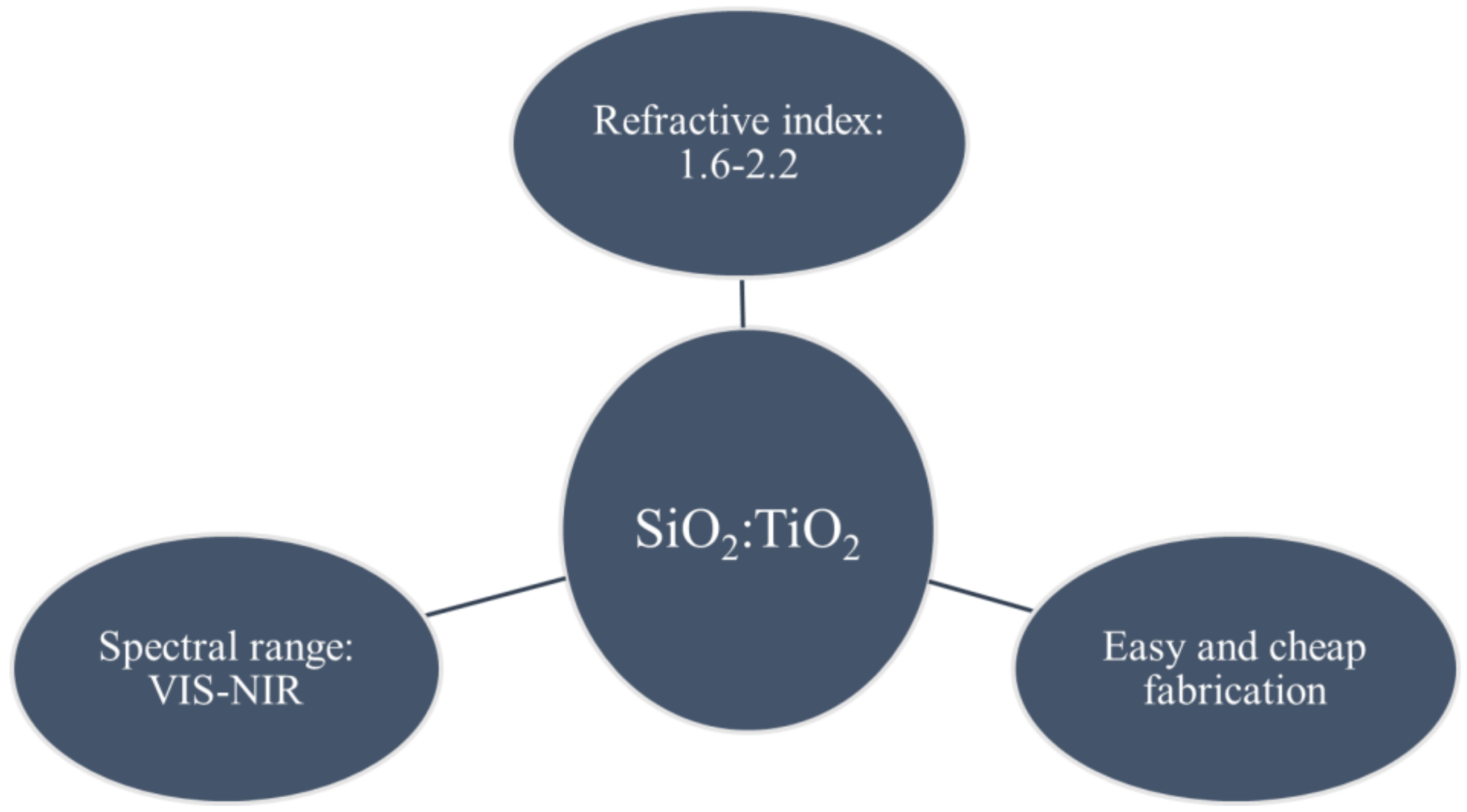
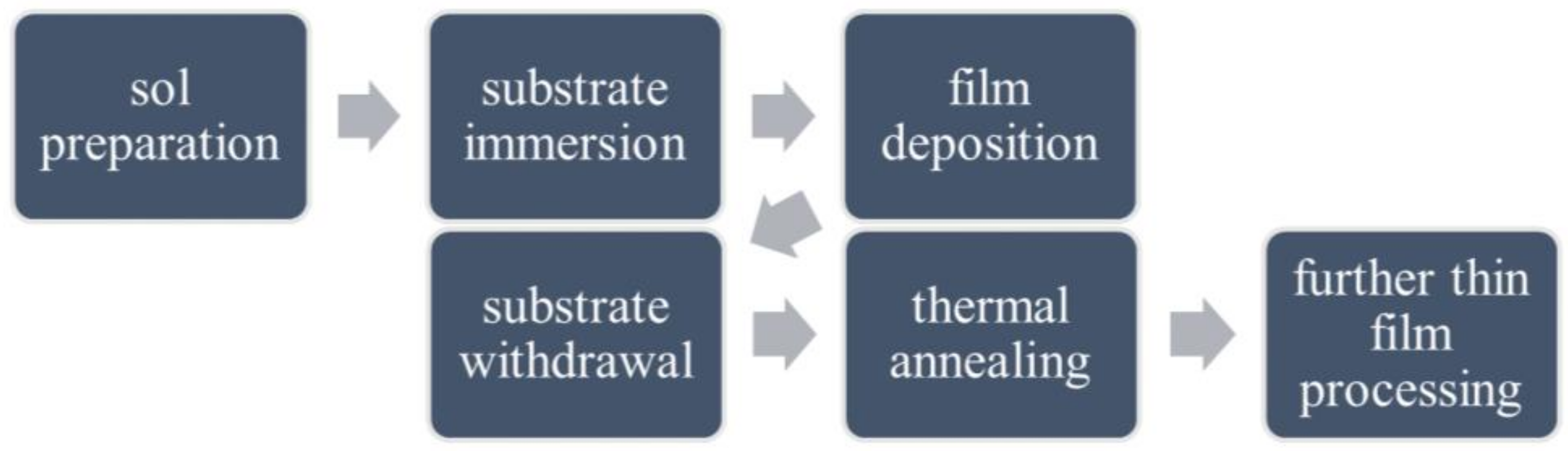
2. Silica-Titania Platform
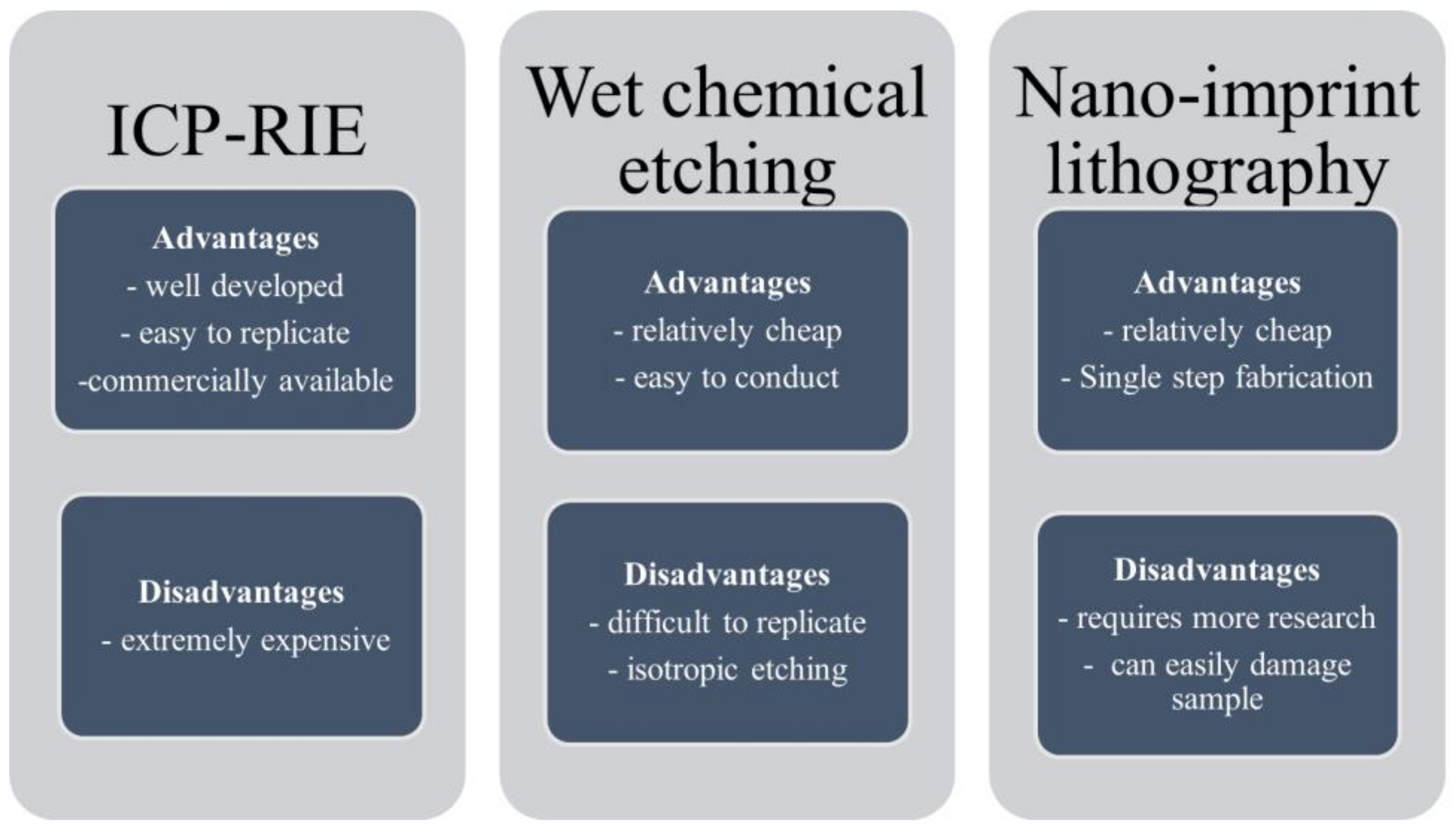
3. Fabrication Processes Under-Development
- Electron-beam (E-beam)/deep UV (DUV) lithography, combined with inductively coupled plasma—reactive ion etching (ICP-RIE)
- Optical lithography combined with wet chemical etching
- Nano-imprint lithography (NIL)
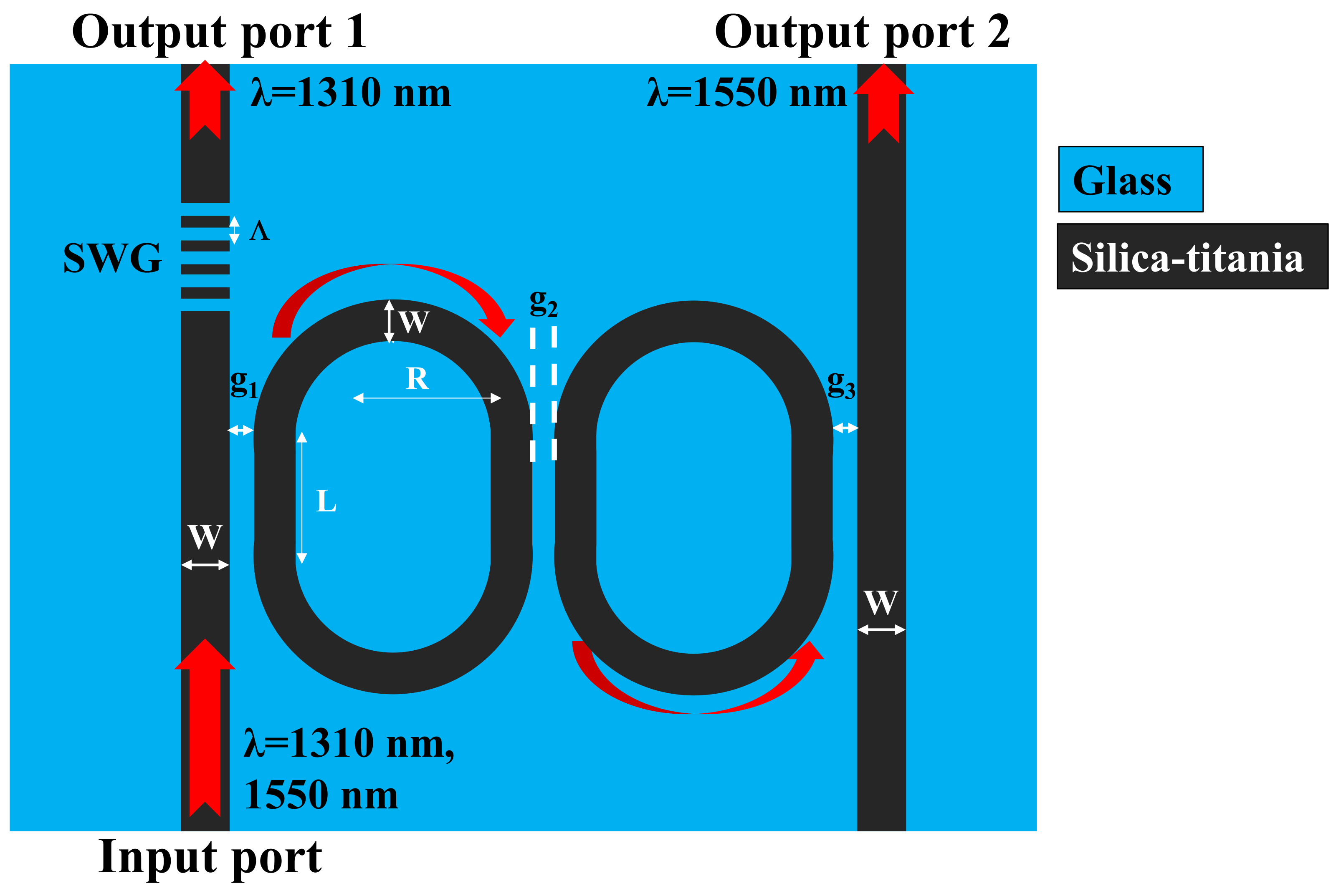
4. Device Design and Numerical Model
5. Conclusions
Author Contributions
Funding
Institutional Review Board Statement
Informed Consent Statement
Data Availability Statement
Acknowledgments
Conflicts of Interest
References
- Sheng, Y.-B.; Zhou, L.; Long, G.-L. One-step quantum secure direct communication. Sci. Bull. 2022, 67, 367–374. [Google Scholar] [CrossRef] [PubMed]
- Khonina, S.; Kazanskiy, N.; Butt, M.; Karpeev, S. Optical multiplexing techniques and their marriage for on-chip and optical fiber communication: A review. Opto-Electron. Adv. 2022, 5, 210127. [Google Scholar] [CrossRef]
- Park, J.; Joo, J.; Kwack, M.-J.; Kim, G.; Han, S.-P.; Kim, S. Three-dimensional wavelength-division multiplexing interconnects based on a low-loss SixNy arrayed waveguide grating. Opt. Express 2021, 29, 35261–35270. [Google Scholar] [CrossRef]
- Pathak, S.; Thourout, D.; Bogaerts, W. Comparison of AWGs and Echelle gratings for wavelength division multiplexing on silicon-on-insulator. IEEE Photonics J. 2014, 6, 4900109. [Google Scholar] [CrossRef]
- Lin, Y.-J.; Lee, S.-L.; Yao, C.-L. Four-channel coarse-wavelength division multiplexing demultiplexer with a modified Mach-Zehnder interferometer configuration on a silicon-on-insulator waveguide. Appl. Opt. 2003, 42, 2689–2694. [Google Scholar] [CrossRef] [PubMed]
- Ahmmed, K.; Chan, H.; Li, B. Three-mode multiplexer and demultiplexer based on the Mach-Zehnder interferometer. OSA Contin. 2021, 4, 1519–1532. [Google Scholar] [CrossRef]
- Menahem, J.; Malka, D. 1 × 4 wavelength demultiplexer C-band using cascaded multimode interference on SiN buried waveguide structure. Materials 2022, 15, 5067. [Google Scholar] [CrossRef]
- Rouifed, M.-S.; Littlejohns, C.; Tina, G.; Qiu, H.; Penades, J.; Nedeljkovic, M.; Zhang, Z.; Liu, C.; Thomson, D.; Mashanovich, G.; et al. Ultra-compact MMI-based beam splitter demultiplexer for the NIR/MIR wavelengths of 1.55 um and 2 um. Opt. Express 2017, 25, 10893–10900. [Google Scholar] [CrossRef]
- Chen, J.; Zhang, Y.; Shi, Y. An on-chip triplexer based on silicon Bragg grating-assisted multimode interference couplers. IEEE Photon. Technol. Lett. 2017, 29, 63–65. [Google Scholar] [CrossRef]
- Xu, Y.; Zhou, W.; Chen, K.; Huang, X. Y-branch wavelength demultiplexer based on topological valley photonic crystals. Opt. Laser Technol. 2022, 155, 108422. [Google Scholar] [CrossRef]
- Prajzler, V.; Mastera, R. Wavelength division multiplexing module with large core optical polymer planar splitter and multilayered dielectric filters. Opt. Quantum Electron. 2017, 49, 133. [Google Scholar] [CrossRef]
- Mehdizadeh, F.; Soroosh, M.; Alipour-Banaei, H. An optical demultiplexer based on photonic crystal ring resonators. Optik 2016, 127, 8706–8709. [Google Scholar] [CrossRef]
- Masilamani, S.; Punniakodi, S. Photonic crystal ring resonator based optical MUX/DEMUX design structures: A survey and comparison study. J. Opt. 2020, 49, 168–177. [Google Scholar] [CrossRef]
- Rakshit, J.; Roy, J. All-optical ultrafast switching in a silicon microring resonator and its application to design multiplexer/demultiplexer, adder/substrator and comparator circuit. Opt. Appl. 2016, XLVI, 517. [Google Scholar]
- Bagheri, A.; Nazari, F.; Moravvej-Farshi, M. Tunable optical demultiplexer for dense wavelength division multiplexing systems using graphene-silicon microring resonators. J. Electron. Mater. 2020, 49, 7410–7419. [Google Scholar] [CrossRef]
- Chang, H.; Kuo, Y.; Jones, R.; Barkai, A.; Bowers, J. Integrated hybrid silicon triplexer. Opt. Express 2010, 18, 23891–23899. [Google Scholar] [CrossRef]
- Xu, H.; Shi, Y. On-chip silicon triplexer based on asymmetrical directional couplers. IEEE Photon. Technol. Lett. 2017, 29, 1265–1268. [Google Scholar] [CrossRef]
- Zhu, N.; Song, J.; Wosinski, L.; He, S.; Thylen, L. Experimental demonstration of a cross-order echelle grating triplexer based on an amorphous silicon nanowire platform. Opt. Lett. 2009, 34, 383–385. [Google Scholar] [CrossRef]
- Butt, M.; Kazanskiy, N.; Khonina, S. Miniaturized design of a 1 × 2 plasmonic demultiplexer based on metal-insulator-metal waveguide for telecommunication wavelengths. Plasmonics 2023. [Google Scholar] [CrossRef]
- Xie, Y.-M.; Lu, Y.-S.; Weng, C.-X.; Cao, X.-Y.; Jia, Z.-Y.; Bao, Y.; Wang, Y.; Yin, H.-L.; Chen, Z.-B. Breaking the rate-loss bound of quantum key distribution with asynchronous two-photon interference. PRX Quantum 2022, 3, 020315. [Google Scholar] [CrossRef]
- Gu, J.; Cao, X.-Y.; Fu, Y.; He, Z.-W.; Yin, Z.-J.; Yin, H.-L.; Chen, Z.-B. Experimental measurement-device-independent type quantum key distribution with flawed and correlated sources. Sci. Bull. 2022, 67, 2167–2175. [Google Scholar] [CrossRef] [PubMed]
- Wu, J.; Long, G.-L.; Hayashi, M. Quantum Secure Direct Communication with Private Dense Coding Using a General Preshared Quantum State. Phys. Rev. Appl. 2022, 17, 064011. [Google Scholar] [CrossRef]
- Zaken, B.; Baruch, B.; Zanzury, T.; Malka, D. An 8-channel wavelength MMI demultiplexer in slot waveguide structures. Materials 2016, 9, 881. [Google Scholar] [CrossRef] [PubMed]
- Tamir, S.; Karanov, N.; Malka, D. 1 × 4 MMI visible light wavelength demultiplexer based on a GaN slot-waveguide structure. Photonics Nanostruct.-Fundam. Appl. 2018, 30, 45–49. [Google Scholar]
- Dhandrapati, L.; Tupakula, S. A novel 8-channel DWDM demultiplexer on silicon photonic crystal slab: Design and analysis. Optik 2022, 256, 168734. [Google Scholar] [CrossRef]
- Naghizade, S.; Sattari-Esfahlan, S. An optical five channel demultiplexer-based simple photonic crystal ring resonator for WDM applications. J. Opt. Commun. 2020, 41, 37–43. [Google Scholar] [CrossRef]
- Chen, J. A broadband wavelength demultiplexer assisted by SWG-based directional couplers. Optik 2020, 202, 163602. [Google Scholar] [CrossRef]
- Wang, F.; Xu, X.; Zhang, C.; Sun, C.; Zhao, J. Design and demonstration of compact and broadband wavelength demultiplexer based on subwavelength grating (SWG). IEEE Photonics J. 2022, 14, 1–6. [Google Scholar] [CrossRef]
- Hao, T.; Sánchez-Postigo, A.; Cheben, P.; Ortega-Moñux, A.; Winnie, N.Y. Dual-band polarization-independent subwavelength grating couplers for wavelength demultiplexing. IEEE Photonics Technol. Lett. 2020, 32, 1163–1166. [Google Scholar] [CrossRef]
- Fukazawa, T.; Fumiaki, O.; Toshihiko, B. Very compact arrayed-waveguide-grating demultiplexer using Si photonic wire waveguides. Jpn. J. Appl. Phys. 2004, 43, L673. [Google Scholar] [CrossRef]
- Hai, M.S.; Leinse, A.; Veenstra, T.; Liboiron-Ladouceur, O. A thermally tunable 1 × 4 channel wavelength demultiplexer designed on a low-loss Si3N4 waveguide platform. Photonics 2015, 2, 1065–1080. [Google Scholar] [CrossRef]
- Butt, M.A.; Kaźmierczak, A.; Tyszkiewicz, C.; Karasiński, P.; Środa, E.; Olszewski, J.; Pala, P.; Martynkien, T.; Hlushchenko, D.; Baraniecki, T.; et al. HYPHa project: A low-cost alternative for integrated photonics. Photonics Lett. Pol. 2022, 14, 25–27. [Google Scholar] [CrossRef]
- Kozlowski, L.; Shahbaz, M.; Butt, M.; Tyszkiewicz, C.; Karasiński, P.; Kazmierczak, A.; Piramidowicz, R. Low-cost Integrated Photonic Platform Developed via a Sol-gel Dip-coating Method: A Brief Review. Sens. Transducers 2022, 259, 82–92. [Google Scholar]
- Butt, M.; Tyszkiewicz, C.; Wojtasik, K.; Karasinski, P.; Kazmierczak, A.; Piramidowicz, R. Subwavelength grating waveguide structures proposed on the low-cost silica-titania platform for optical filtering and refractive index sensing applications. Int. J. Mol. Sci. 2022, 23, 6614. [Google Scholar] [CrossRef]
- Karasinski, P. Sol-gel derived optical waveguide films for planar sensors with phase modulation. Opt. Appl. 2004, 34, 467–475. [Google Scholar]
- Karasinski, P.; Jaglarz, J.; Mazur, J. Low loss silica-titania waveguide films. Photonics Lett. Pol. 2010, 2, 37–39. [Google Scholar]
- Racka-Szmidt, K.; Stonio, B.; Zelazko, J.; Filipiak, M.; Sochacki, M. A review: Inductively coupled plasma reactive ion etching of silicon carbide. Materials 2022, 15, 123. [Google Scholar] [CrossRef] [PubMed]
- Park, H.; Cho, J.; Jung, J.; Duy, P.P.; Le, A.; Yi, J. A review of wet chemical etching of glasses in hydrofluoric acid based solution for thin film silicon solar cell application. Curr. Photovolt. Res. 2017, 5, 75–82. [Google Scholar]
- Chen, Y.; Shu, Z.; Zhang, S.; Zeng, P.; Liang, H.; Zheng, M.; Duan, H. Sub-10 nm fabrication: Methods and applications. Int. J. Extrem. Manuf. 2021, 3, 032002. [Google Scholar] [CrossRef]
- Kazanskiy, N.L.; Butt, M.; Khonina, S.N. Silicon photonic devices realized on refractive index engineered subwavelength grating waveguides-A review. Opt. Laser Technol. 2021, 138, 106863. [Google Scholar] [CrossRef]
- Khonina, S.N.; Kazanskiy, N.L.; Butt, M.A. Spectral characteristics of broad band-rejection filter based on Bragg grating, one-dimensional photonic crystal, and subwavelength grating waveguide. Phys. Scr. 2021, 96, 055505. [Google Scholar] [CrossRef]


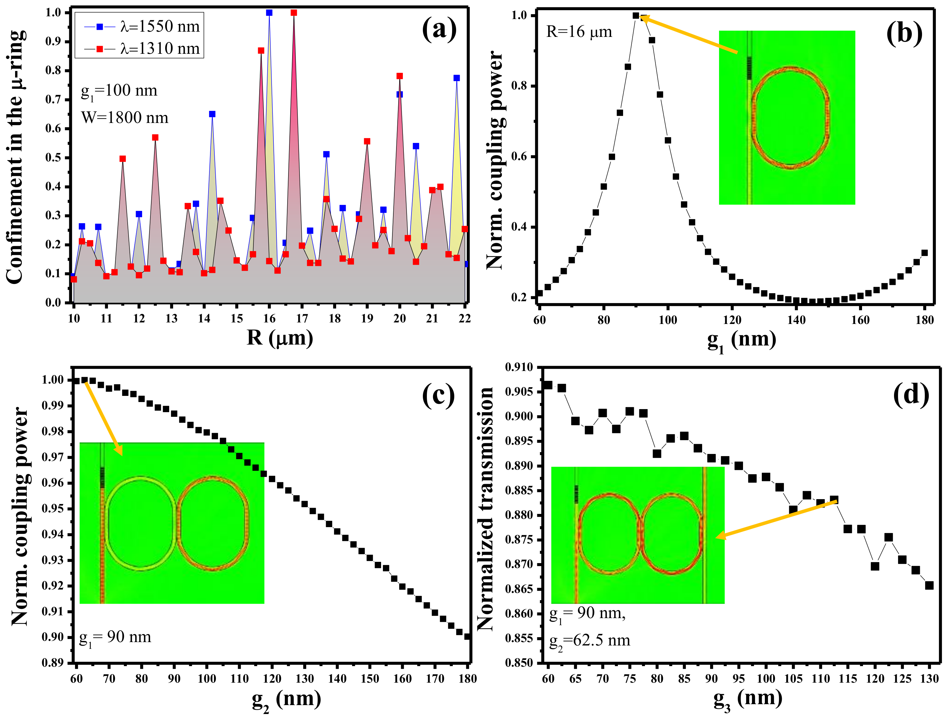
| Parameter | Values |
|---|---|
| W | 1800 nm (fixed) |
| R | 10–22 μm (range) |
| L | 10 μm (fixed) |
| g1 | 80–180 nm (range) |
| g2 | 80–370 nm (range) |
| g3 | 60–120 nm (range) |
| Operational wavelength | 1310 and 1550 nm (fixed) |
| Footprint | 84 μm × 125 μm |
| ʌ = a + b, where b = 250 nm | 350–850 nm (range) |
| N | 15 |
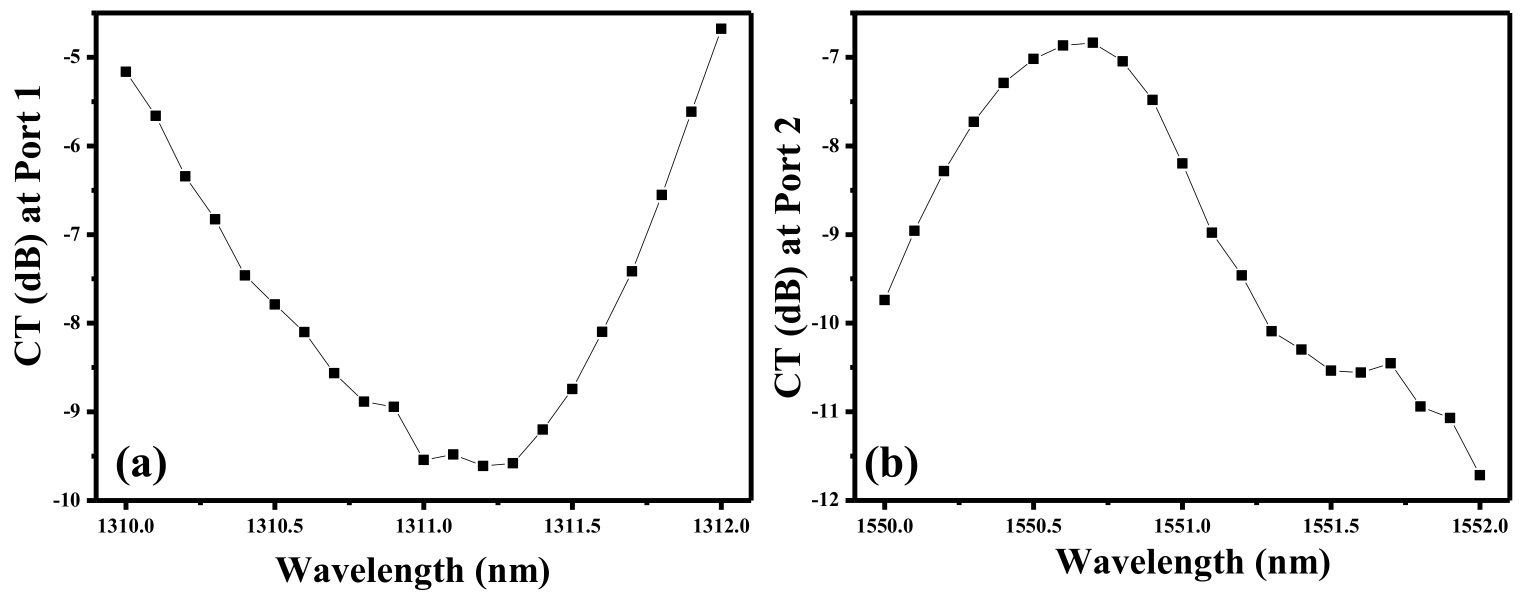
| Design | Cross Talk at Output Port 1 (dB) | Cross Talk at Output Port 2 (dB) |
|---|---|---|
| Demultiplexer without SWG | −1.6 | −9.23 |
| Demultiplexer with SWG | −6.6 | −9.04 |
| Ref. | Material | Design | Wavelength (nm) | Numerical/ Experimental | CT (dB) | Footprint |
|---|---|---|---|---|---|---|
| [23] | GaN, Si | MMI | 1530–1565 | Numerical | −19.97 to −13.77 | - |
| [24] | GaN, Si | MMI | 547–584 | Numerical | 13.8–18.3 dB | - |
| [25] | Si | PhC, RR | 1535–1539 | Numerical | −18.31 | - |
| [26] | Si | RR | 1550–1567 | Numerical | −13–−24 | 689.61 (μm2) |
| [27] | SOI | SWG | 1310, 1550 | Numerical | - | - |
| [28] | SOI | SWG | 1310, 1550 | Experimental | - | - |
| [29] | SOI | SWG | 1310, 1550 | Numerical | - | - |
| [30] | SOI | AWG | 1500–1570 | Experimental | - | 110 × 93 (mm2) |
| [31] | Si3N4 | MZI | 1530–1580 | Experimental | 14.5 | - |
| This work | SiO2:TiO2 | RR | 1550, 1310 | Numerical | −6.6 and −9.04 | 84 μm × 125 μm |
Disclaimer/Publisher’s Note: The statements, opinions and data contained in all publications are solely those of the individual author(s) and contributor(s) and not of MDPI and/or the editor(s). MDPI and/or the editor(s) disclaim responsibility for any injury to people or property resulting from any ideas, methods, instructions or products referred to in the content. |
© 2023 by the authors. Licensee MDPI, Basel, Switzerland. This article is an open access article distributed under the terms and conditions of the Creative Commons Attribution (CC BY) license (https://creativecommons.org/licenses/by/4.0/).
Share and Cite
Butt, M.A.; Shahbaz, M.; Kozłowski, Ł.; Kaźmierczak, A.; Piramidowicz, R. Silica-Titania Integrated Photonics Platform-Based 1 × 2 Demultiplexer Utilizing Two Serially Cascaded Racetrack Microrings for 1310 nm and 1550 nm Telecommunication Wavelengths. Photonics 2023, 10, 208. https://doi.org/10.3390/photonics10020208
Butt MA, Shahbaz M, Kozłowski Ł, Kaźmierczak A, Piramidowicz R. Silica-Titania Integrated Photonics Platform-Based 1 × 2 Demultiplexer Utilizing Two Serially Cascaded Racetrack Microrings for 1310 nm and 1550 nm Telecommunication Wavelengths. Photonics. 2023; 10(2):208. https://doi.org/10.3390/photonics10020208
Chicago/Turabian StyleButt, Muhammad A., Muhammad Shahbaz, Łukasz Kozłowski, Andrzej Kaźmierczak, and Ryszard Piramidowicz. 2023. "Silica-Titania Integrated Photonics Platform-Based 1 × 2 Demultiplexer Utilizing Two Serially Cascaded Racetrack Microrings for 1310 nm and 1550 nm Telecommunication Wavelengths" Photonics 10, no. 2: 208. https://doi.org/10.3390/photonics10020208