Article

Angle-Based Parametrization with Evolutionary Optimization for OESCL-Band Y-Junction Splitters

by
Roy Prosopio-Galarza
1,†,
J. Leonidas García-Gonzales
2,†,
Freddy Jara
1,
Maria Armas-Alvarado
1,2,
Jorge Gonzalez
2 and
Ruth E. Rubio-Noriega
1,*
1
Group of Radiofrequency Microwave and Optics (G-RFMO), National Institute for Research and Training in Telecommunications (INICTEL), National University of Engineering (UNI), Lima 15001, Peru
2
Computer Engineering Group (CEG), Computer Science Department, University of Engineering and Technology (UTEC), Lima 15001, Peru
*
Author to whom correspondence should be addressed.
These authors contributed equally to this work.
Photonics 2023, 10(2), 152; https://doi.org/10.3390/photonics10020152
Submission received: 11 December 2022 / Revised: 18 January 2023 / Accepted: 26 January 2023 / Published: 1 February 2023
(This article belongs to the Topic Optical and Optoelectronic Materials and Applications)
(This article belongs to the Section Optical Communication and Network)

Abstract

:
The design of passive photonic devices based on geometry optimization can lead to energy-efficient, small-footprint, and fabrication-ready geometries. In this work, we propose an angle-based parametrization method to optimize Y-junction splitters based on multimode interferometers. The selected figure of merit was the transmittance in the SCL and OESCL optical fiber communication bands. The performances of three optimization methods were compared: (i) particle swarm optimization (PSO), (ii) genetic algorithm (GA), and (iii) the covariance matrix adaptation-evolution strategy (CMA-ES). The results show that CMA-ES parametrization produces similar transmittance results (≤1.5% of difference) to PSO in the first 40 generations. The CMA-ES results are identical in the SCL (1460–1625 nm) and OESCL (1260–1625 nm) bands, whereas the GA and PSO executions are slightly different in terms of the rate and similarity of the figure of merit.

1. Introduction

Photonic integrated circuits (PICs) enable the interconnection of different types of photonic devices into a single platform. Designing energy-efficient on-chip optical interconnects remains a challenge when scaling the number of devices per chip [1]. Many optical passive devices work traditionally in the SCL optical communications band, while the OESCL band has gained attention due to ultra-wideband applications [2].
Among the passive components on a chip, the 3 dB power splitters are present in the order of dozens [3,4,5]. A 3 dB power splitter distributes the signal across multiple optical interconnects and is the essential building block for switches [6,7], modulators [8,9], and multiplexers [10,11]. Y-junctions based on multi-mode interferometers have become one of the essential building blocks in photonic integrated circuits [12]. Moreover, many inverse design methodologies for power splitters are based on multi-mode interferometer Y-junctions [10,12,13].
There are three main causes for excess loss in fabricated Y-junctions [12,14]: (i) a low tolerance to fabrication errors, (ii) minimum fabricated resolution available, and (iii) deviations in the sharp angles (see α i in Section 2.1). Special mask techniques can to help overcome these problems, e.g., the electron beam technique [13,14]. In this regard, any device geometry, regardless of the type of optimization, has to be adjusted to the fabrication tolerances of the machinery available to the designer. This is especially true for non-intuitive geometries generated by optimization methods. Post-processes are usually added [13,15], in which the fabrication constraints are fed to a second algorithm to smooth and tweak the optimized geometry, making it fabrication-ready.
Figure 1 shows the timeline of some popular optimization algorithms used in the photonic design and relates them to their adoption (by the number of citations). We observe that the most popular algorithms are particle swarm optimization (PSO) [16] and genetic algorithms (GAs) [17]. These algorithms are usually used with default parameters due to the computational complexity of performing a hyperparameter optimization, which can limit their performance [18]. The covariance matrix adaptation evolution strategy (CMA-ES) [19] is a global optimization algorithm that has not been widely adopted. However, it does not need to optimize its parameters—only its population size. This characteristic is important because increasing the population size usually leads to a more exhaustive search. Furthermore, CMA-ES has been demonstrated to be efficient, robust, and easy for antenna optimization [20]. This motivates us to compare the performance and convergence of CMA-ES, GA, and PSO.
Figure 1 includes other optimization methods: (i) moving asymptotes (MMA) [21], (ii) limited memory Broyden–Fletcher–Goldfarb–Shanno bound constrained (L-BFGS-B) [22], and (iii) differential Evolution (DE) [23]. For a detailed review on optimization methods, please refer to [18,24,25].
Table 1 shows examples of photonic splitters designed using different algorithms to those presented in this work. Our CMA-ES-based optimized splitter presents a wider bandwidth along with a shorter footprint, and we also expect lower losses.
Our work extends an angle-based parametrization [26]. It defines the device’s internal angles and requires fewer parameters than conventional topological optimization because its number of parameters depends on one dimension of the design space. In contrast, conventional topology optimization relies on two design space dimensions. Then, the optimization of the device is reduced to a medium-dimensional problem, allowing us to use global optimization [18]. The usage of global optimization is a key difference compared to other approaches, such as level-set and density topology, which usually rely only on local optimization [9,24,27].
To the best of our knowledge, we propose the first strict comparison of (i) the waveband analysis, (ii) convergence rate, and (iii) similarity of the figure of merit between three different executions of GA, PSO, and CMA-ES to provide PIC designers with adequate tools for fabrication-ready ultra-broadband 3 dB MMI (multi-mode interferometer) power splitters.

2. Angle-Based Parametrization

Our goal is to propose a parametrization that achieves functional devices with a high tolerance to fabrication errors (i) using a lower quantity (∼15) of parameters compared to the conventional methods, and (ii) by avoiding sharp angles.

2.1. Materials and Methods

We used a silicon-on-insulator (SOI) platform, which is extremely attractive because of its compatibility with microelectronics, introducing now-popular scalable photonic integrated circuits.
In the inverse design, we need to specify the permittivity distribution via parametrization. The most used methods are (i) the density topology and (ii) level-set. In both methods, the design region is divided into pixels, and a permittivity is associated to each pixel [24]. For more methods, please refer to [34].
A drawback of these methods is that they usually require a high number of parameters to have the flexibility of exploring desired fabricable devices. The higher the degrees of freedom, the better we can explore the designs. However, this process can require considerable computing resources (i.e., CPU- or memory) [18], leading to significant execution times.
We propose the angle-based parametrization depicted in Figure 2. The pink region depicts the silicon core and the white background color represents silicon oxide. We divided a rectangular MMI splitter design region into z equally spaced vertical-aligned segments. The segments have different widths. Therefore, the division gives us a set of angles between consecutive segments, where α i | 1 p are the angles and optimization parameters, and p = z 1 .
The waveguide width W g , MMI body length, L M M I , and gap δ can be adjusted to fit multiple outputs or operation frequencies. For simplicity, we demonstrate a 1 × 2 splitter working at 1550 nm.
A 1 × 2 MMI splitter parametrization can be summarized in three main steps:
(i)
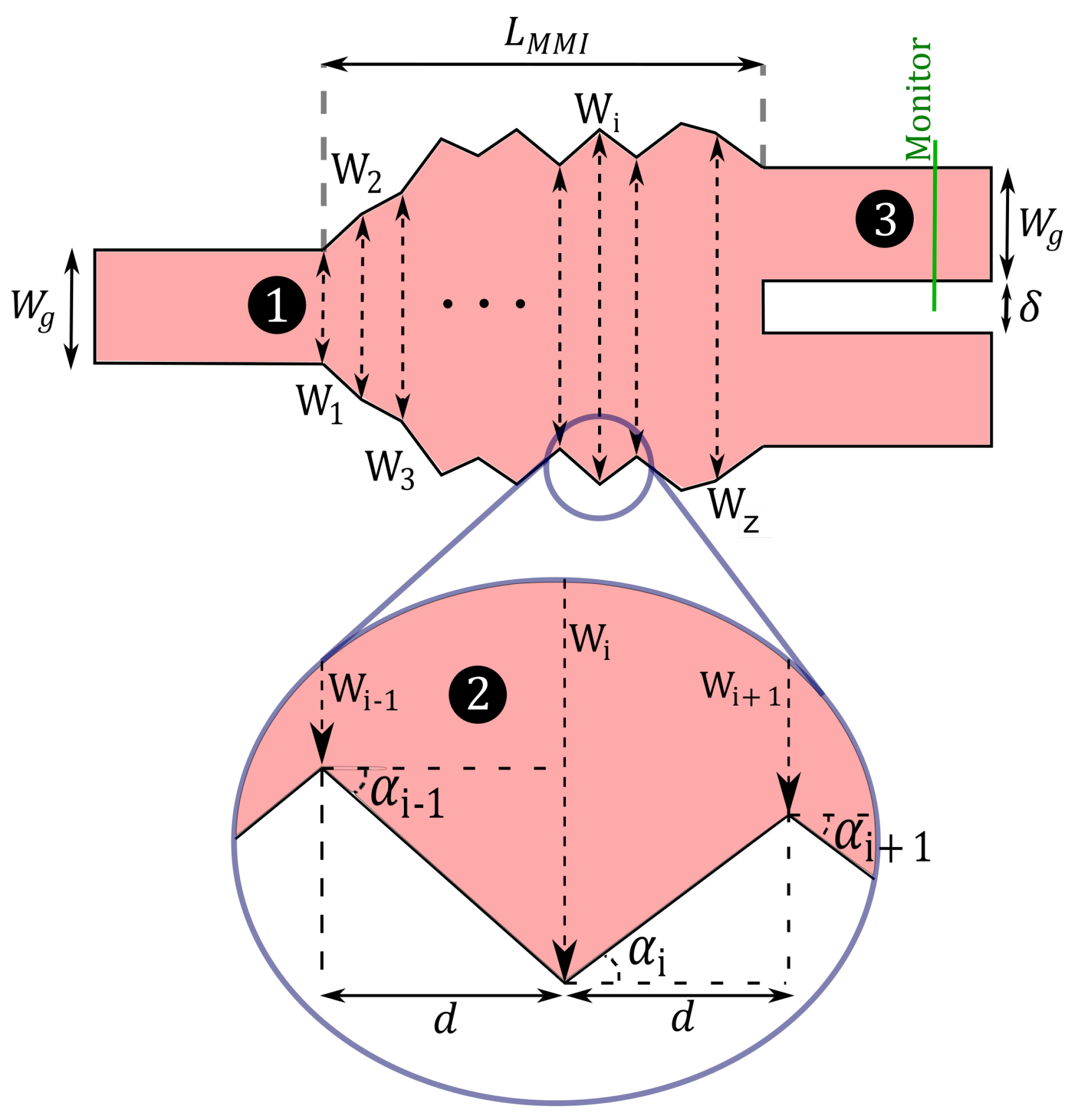
First, we divide the initial topology into W i [ i = 1 z ] longitudinal equally spaced segments 1 based on [12,35,36], and we set symmetry on the transverse direction of the propagation. We also set the values of δ = 0.2 μ m and L M M I = 2 μ m. This allows us to reduce the number of angles α i to optimize because the angles on the upper edge of the device match those at the bottom edge.
(ii)
Second, we modify the dimensions of the current width W i 2 based on the previous width and angle, as shown in Equation (1). In particular, we can set W 1 = W g = 0.5 μ m for the 1550 nm working window.
W i = W i 1 + 2 d · tan ( α i 1 ) for i > 1
(iii)
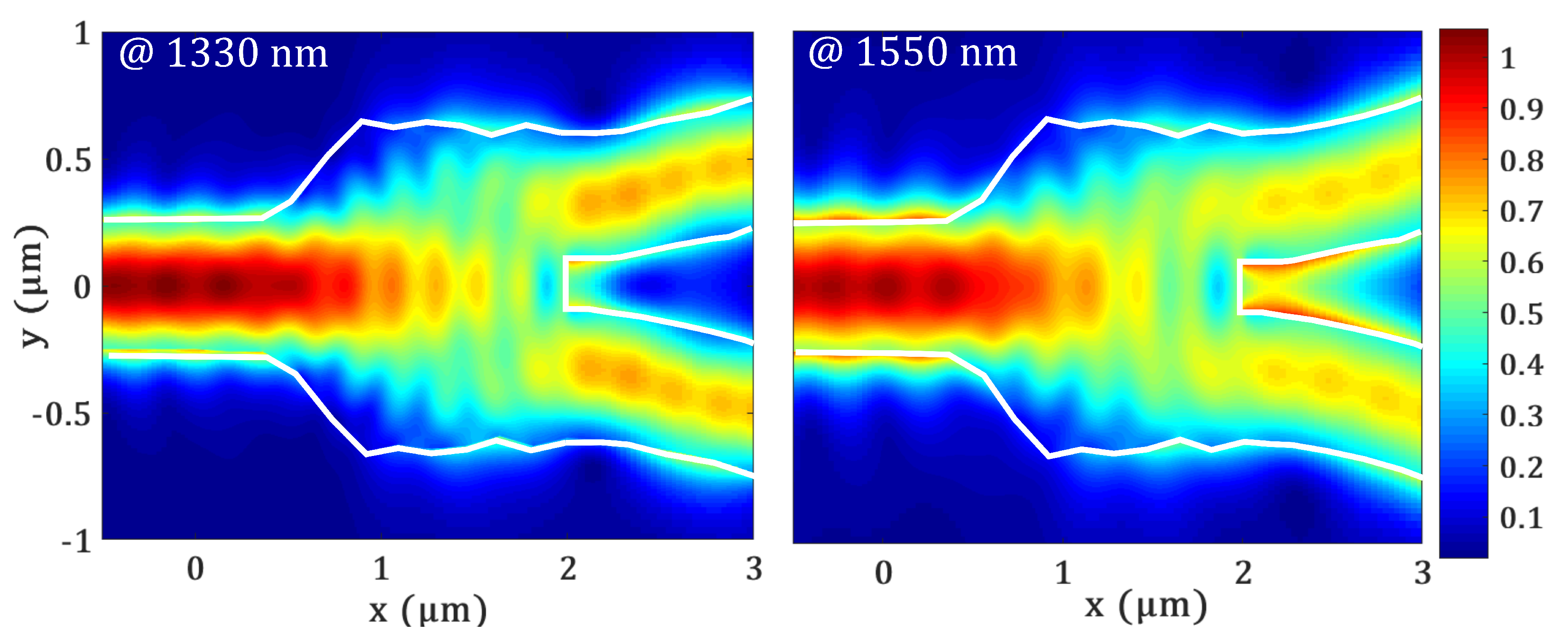
Third, we place a power monitor 3 at one waveguide output to measure the transmittance of the fundamental TE (transverse electric) mode in order to establish the figure of merit.

2.2. Figure of Merit (FOM)

The choice of an FOM is the most critical parameter on the optimization setup. The FOM is a value used to characterize the performance of the design. We evaluated the Y-junctions efficiency by the transmittance over a set bandwidth. To improve transmittance without affecting the area on-chip, we limited the size of the MMI by restricting the parameter range of the angles and setting an FOM directly proportional to the transmittance of the fundamental TE mode over a frequency window. We ran the optimizations over SCL (conventional) and OESCL (wide) bands to obtain MMI geometries and evaluated the performance.
Our goal is to maximize the FOM. Let T ( f ) be the transmittance evaluated at the frequency f. We propose the FOM as the transmittance accumulated from f 1 to f 2 shown in Equation (2).
F O M = f 1 f 2 T ( f ) d f
where f 1 = c λ 1 , f 2 = c λ 2 , the frequency is in Terahertz, and c is the speed of light in the vacuum. The values of λ 1 and λ 2 depend on the operating band. We define two FOMs:
(i)
For the S C L band, λ 1 = 1.625   μ m and λ 2 = 1.46   μ m. The ideal value for the FOM is 10.425 assuming rectangular transmittance windows with a maximum amplitude of 50% on one output waveguide along the SCL band.
(ii)
For the O E S C L band, λ 1 = 1.625   μ m and λ 2 = 1.26   μ m. The ideal value for the FOM is 26.721 assuming a transmittance of 50% on one output waveguide along the OESCL band.
Although it is more geometry-restrictive than density topology and level-set parametrization, our approach shows promising results and potential for improvements (see Section 4). We produced fabrication-ready devices without any additional post-processing steps for smoothing or tweaking the optimized geometry. In the same fashion, other fabrication constraints can be morphed into optimization parameters, as we propose here, to produce faster and direct results.

3. Optimization Algorithms

This section details the three evolutionary algorithms used in this work: (i) GA, (ii) PSO, (iii) CMA-ES. Our implementations of these algorithms are used to independently optimize the two FOMs defined in Section 2.

3.1. Genetic Algorithm

GA is a metaheuristic inspired by the process of natural selection [17], and GA is used for the design of novel optic devices such as (i) polarization beam splitters [37,38] and (ii) Y-branch waveguides [27,33,39].
As depicted in Algorithm 1, GA has four main steps. First, it starts with n individuals represented by p parameters. Second, it will simulate the evolution of these individuals during k generations. In each generation, the simulation starts selecting a set of individuals to survive; those are called parents. Third, parents are combined following a crossover policy to produce n new individuals that share some parameters with the selected parents. Finally, the individuals randomly mutate some of their parameters.
Algorithm 1 depicts our implementation, with the following method specifications:
Algorithm 1: Framework of GA
Photonics 10 00152 i001
  • g e n e r a t e _ p o p u l a t i o n ( n , p ) : returns n vectors defined by p angles ( α i , i [ 1 , p ] defined in Section 2 with random values from a uniform distribution in the range of the constrains of each parameter.
  • s e l e c t ( p o p u l a t i o n ) : chooses q individuals (i.e., we use roulette wheel selection) depending on the probability value p r o b i given by Equation (3):
    p r o b i = F O M i m i n ( F O M ) ( F O M j m i n ( F O M ) )
    where F O M i is associated with the i-th individual.
  • c r o s s o v e r ( p o p u l a t i o n , p a r e n t s ) : returns n vectors of dimension p. The i-th vector is the combination of two random parents p a i and p b i selected from p a r e n t s . Its d-th parameter is defined at random by p a i , d or p b i , d with equal probability (i.e., we are using uniform crossover). This generates new combinations of angles to be evaluated.
  • m u t a t i o n ( c h i l d r e n ) : returns the new combinations of the previous step, but each individual may have some of its parameters added a random value u U ( r , r ) . This updates the angles α i of each individual.

3.2. Particle Swarm Optimization

In [16], the authors proposed PSO to simplify the social behavior of a flock of birds. It has shown success in discontinuous multidimensional problems in electromagnetism applications [18,20,27]. The PSO algorithm is similar to GA, but the i-th individual is related to a number ν ( i ) and a p-dimensional vector x b e s t ( i ) .
We can think of the i-th individual as a particle defined by: (i) its position x ( i ) (the p-dimensional vector associated with the individual), (ii) its velocity ν ( i ) , and (iii) the best position the particle has found so far, named x b e s t ( i ) . Each particle accumulates speed in a favorable direction given by the best position found by the particle and the best position globally found. As a result, particles can move independently of local perturbations. By adding random walks, the particles can move in unpredictable ways that can potentially find better directions.
Using the framework of Algorithm 1, we can describe PSO methods as follows:
  • g e n e r a t e _ p o p u l a t i o n ( n , p ) : returns n particles defined by p angles ( α i , i [ 1 , p ] ) defined in Section 2, where its attributes have random values from a uniform distribution in the range of the constraints of each parameter.
  • s e l e c t ( p o p u l a t i o n ) : returns the particle with the best FOM.
  • c r o s s o v e r ( p o p u l a t i o n , p a r e n t s ) : returns the population updated with the use of Equation (4) (this updates the angles α i , i [ 1 , p ] of each of the n particles) and Equation (5):
    x ( i ) x ( i ) + ν ( i )
    ν ( i ) ω ν ( i ) + c 1 r 1 x b ( i ) x ( i ) + c 2 r 2 x b x ( i )
    where x b is the best position globally found, ω , known as inertia weight, represents the will of the particle to conserve its current velocity, c 1 and c 2 quantify the relative attraction of x b ( i ) and x b , respectively, and r 1 , r 2 U ( 0 , 1 ) represent the unpredictable behavior.

3.3. Covariance Matrix Adaptation Evolution Strategy

CMA-ES [19] is an evolutionary strategy that has shown promising results for the design of antenna devices [20], splitting/combining [40], and grating filters [41]. The general idea of CMA-ES, shown in Algorithm 2, is to maintain: (i) an p-dimensional vector μ where p is the number of parameters (i.e., number of angles), (ii) a matrix C, and (iii) a number σ to generate n sample points from a distribution N ( μ , σ 2 C ) .
Algorithm 2: CMA-ES algorithm
Photonics 10 00152 i002
Taking points from this distribution limits the search space to a hyperellipse. Then, the algorithm evaluates points from the hyperellipse. Using the obtained values, it can decide to: (i) move the hyperellipse to another search space region and (ii) expand or reduce the covered region. CMA-ES works iteratively on this idea until the hyperellipse almost degenerates to a point, which is potentially the global optimum. For a detailed description of the algorithm, please refer to [42].
In Algorithm 2, we consider global variables for the sake of simplicity. We summarize CMA-ES in five steps. In line 1, we repeat the same procedures k times. In iteration t, we start with line 2 sampling n random p dimensional (each dimension corresponds to an angle α i defined in Section 2) points x i , where x is sorted in descending order by evaluating the FOM. The points are obtained from the distribution N ( μ , σ 2 C ) . The next steps update the parameters μ , σ , and C such that we can evaluate different angle parametrizations (potentially with better FOM values) in the next iterations. In line 3, we update the mean μ using a weighted average of the sample points; see Equation (6).
μ ( t + 1 ) i = 1 n w i x i
The coefficients w i are fixed and chosen to proportionate larger contributions to the best-performing points; then, the mean μ is moved to a favorable region. Next, we need to properly change σ to reduce or expand the hyperellipse of the next iteration. Therefore, in line 4, we control σ using Equations (7) and (8).
σ ( t + 1 ) σ ( t ) exp c σ d σ | | p σ | | E | | N ( 0 , I ) | | 1 evolution path comparison
E | | N ( 0 , I ) | | = 2 Γ p + 1 2 Γ p 2
where p σ is a cumulative variable that tracks steps over time, c σ [ 0 , 1 ] is a variable that determines the cumulation time for p σ , and d σ 1 is a damping parameter that determines the possible rate of change in σ ( t + 1 ) . The key part of Equation (7) is the evolution path comparison; here, the length of p σ is compared to its expected length under random selection. From this comparison, we can control σ as increasing, decreasing, or keeping its value. Finally, in line 5, we change Σ in a favorable direction using Equation (9).
C ( t + 1 ) = 1 c 1 c c ( 1 h σ ) ( 2 c c ) c 1 c μ C ( t ) cumulative update + c 1 p C p C T rank - one update + c μ i = 1 n w i δ ( i ) δ ( i ) T rank - μ update
where c μ 1 is the learning rate for the rank-μ update, c 1 1 c μ is the learning rate for the rank-one update, c c [ 0 , 1 ] is the learning rate for the cumulative update, h σ is the evaluation of a unit step function used to properly update the evolution path, p C is a cumulative vector used to update the covariance matrix, w i is a modification of the coefficients w i , and δ ( i ) is the sampled deviations.
In Equation (9), the first term (cumulative update) retains the information of the previous covariance matrix. The second term (rank-one update) allows for elongating the distribution along a favorable axis. The third term (rank-μ update) increases the search in areas where good solutions are likely to exist. The combination of the three terms changes C to move the hyperellipse in a favorable direction.

3.4. Algorithm’s Implementation

Our angle-based method (Section 2) was optimized with each of the algorithms using the parameters in Table 2 following the variables described in the three previous sections. We used p = 11 angles to parametrize the splitter. For the optimization, we executed the algorithms k = 100 times and each step works with n = 40 exploratory designs. The parameter r is described in Section 3.1 and the parameters ω , c i in Section 3.2.
Let us impose the non-optimized geometry limits of our 3 dB Y-junction: a 2000 nm long and 1500 nm wide rectangular multi-mode interferometer (when α i = 0 and all W i are the same). Thus, using p = 11 the feature size of each subsegment is well above 120 nm, which is the limit of fabrication of many UV-lithography processes even by multi-project wafer standards [43].

4. Results

We executed each algorithm with a fixed number of iterations using the parameters in Table 2. The executions were run three times in the bands SCL for commonly optical interconnected applications and OESCL for ultra-wideband applications. We used this differentiated frequency window approach to test the robustness of the transmittance integral defined in Equation (2). Lumerical’s 2.5D variational FDTD was run on the solutions. All optimized designs depend on the initial population and thus on the initial guess. Before our work evaluation, we performed an exploratory analysis for validation, executing an optimization for all algorithms four times each. This was performed individually with a different initial random guess because we do not want to make additional assumptions about the final design and wanted to simply let the optimization algorithms find some patterns.
Our results are presented in three main terms:
(i)
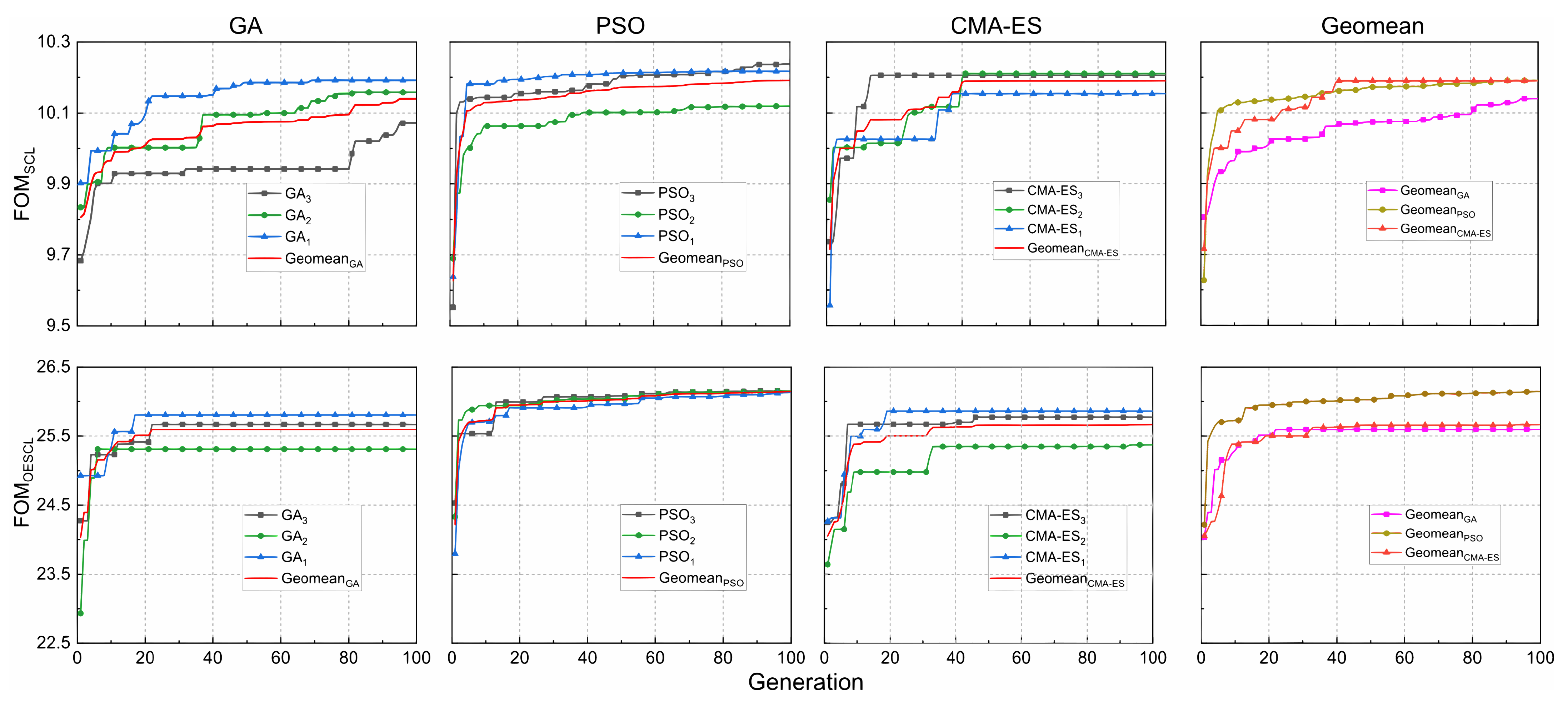
Convergence rate is the algorithm’s speed in achieving FOM stability, with a variation <2%. To calculate it, we used the mean (Geomean) of the FOM trend.
(ii)
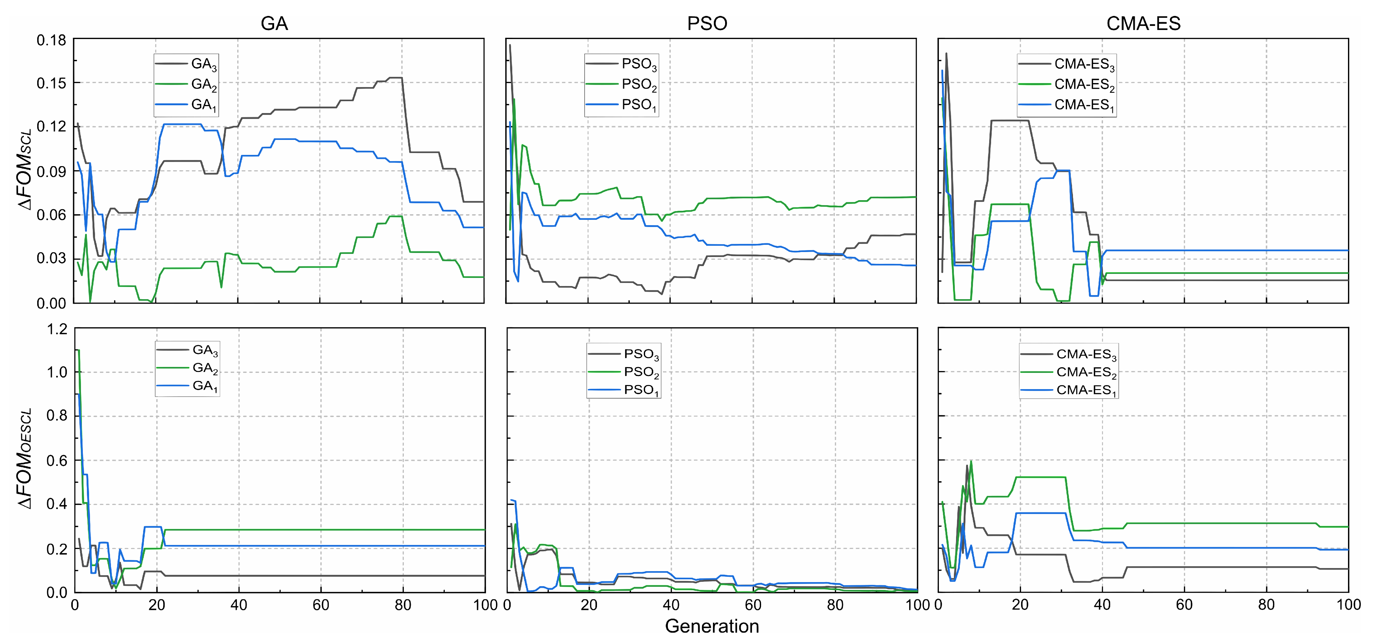
To evaluate the similarity of the FOM, we defined the deviation factor Δ F O M as the absolute difference between the geometric mean, Geomean, and the actual FOM trend value, Δ F O M i , j = | Geomean i F O M i , j | , where j is each algorithm execution, i.e., PSO 1 , PSO 2 , and PSO 3 , and i is the type of algorithm, i.e., Geomean P S O , Geomean G A , or Geomean C M A E S . Additionally, the maximum FOM was also considered to characterize the performance of each method.
(iii)
The waveband analysis was performed over a defined band, either SCL or OESCL. We analyzed the maximum and minimum transmittance values to characterize a planar response of the device over the given frequency. We considered variations ≤1% of the transmittance to be under the fabrication error limit.
The average optimization total execution time was 12 h for a 100-iteration analysis for each algorithm. Our experiments were performed on an individual workstation with an Intel i7 processor 4th gen and 32 GB of RAM.

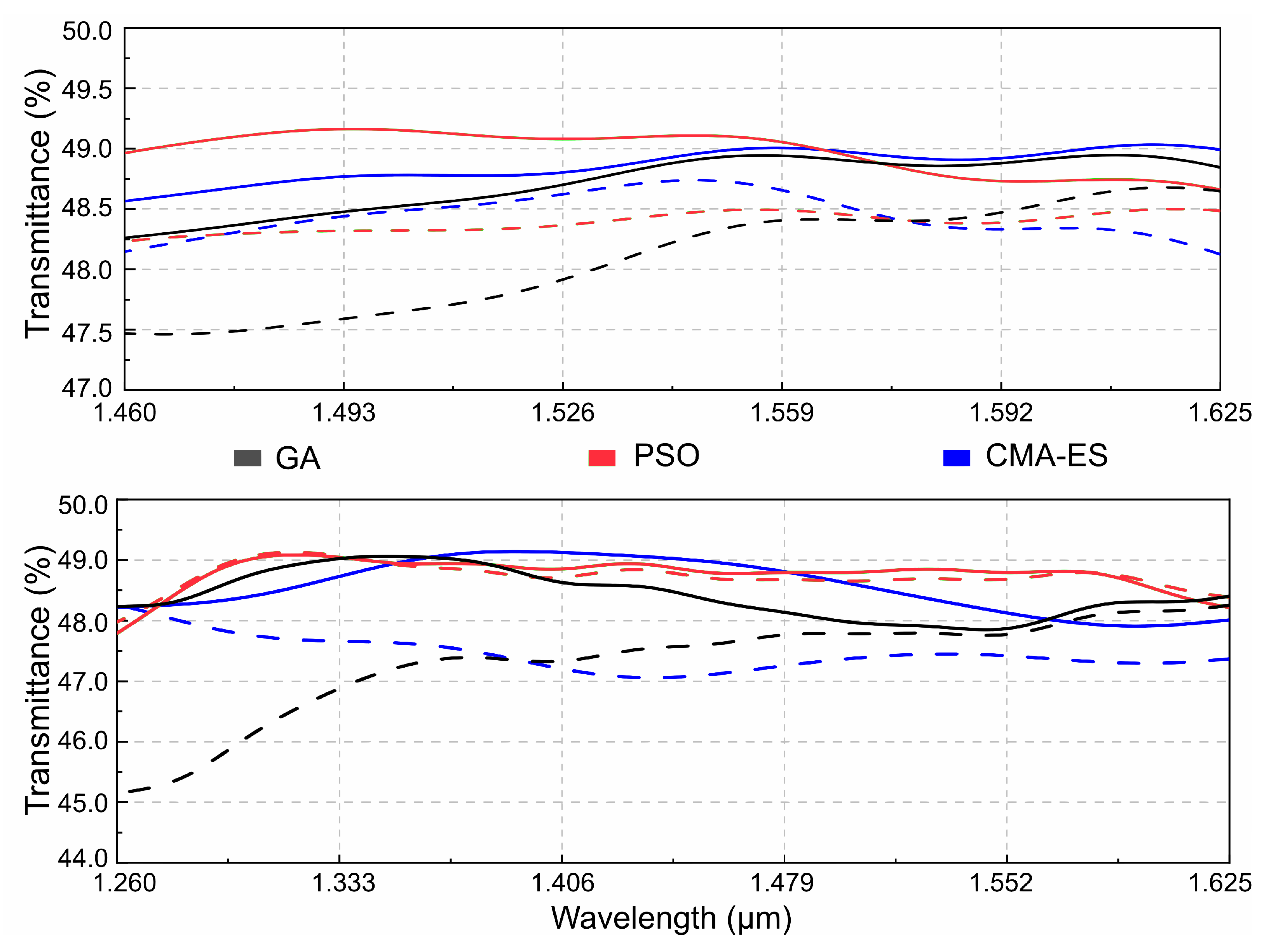
4.1. Convergence Rate

Figure 3 depicts the FOM trend for each optimization run over the SCL (top) and OESCL (bottom) bands. From Figure 3 (top), we make two key observations regarding the Geomean. First, Geomean C M A E S shows that CMA-ES is the fastest algorithm, converging at the 40th generation. Notice that PSO has a high initial growth rate; however, the <2% criteria is only met in the 71st iteration. Second, GA exhibits the slowest convergence rate; it converges at the ∼90th iteration, obtaining the lowest FOM.
From Figure 3 (bottom), we make three observations. First, in the OESCL band, the fastest method, regardless of its maximum FOM (25.6), is the GA, which converges at the 20th generation. However, as seen here and in the SCL analysis, the FOM values constantly get stuck. This is a drawback for the GA, even after 100 generations. Second, Geomean C M A E S achieves a maximum FOM at the 42nd generation; however, its maximum is just behind that of Geomean P S O . Lastly, the PSO algorithm achieved a maximum FOM over 26, which is greater than FOM GA at the ∼50th generation.
We conclude that the CMA-ES algorithm is the fastest and has a similar FOM to PSO in the SCL-band analysis. In the OESCL-band, its maximum FOM decays ∼2% in relative amplitude, and its convergence rate stays almost the same at the ∼40th generation. This consistency is a desirable feature for a global optimization algorithm.

4.2. Similarity of the FOM

We expect that Δ F O M decreases as the number of iteration increases; however, this is not the case for the GA in the SCL band depicted in Figure 4 (top). From this figure, we make two key observations. First, GA has the most dissimilar FOM trends among its three executions. Each GA execution finds a different best parametrization multiple times through its 100 generations. Second, CMA-ES and PSO have a clear stabilization of Δ F O M . This is especially true for CMA-ES after the 40th generation. The similarity of the FOM is down to 0.05, and this result constitutes the best one for the SCL band analysis.
From Figure 4 (bottom), we make the following observations. First, the PSO has the best similarity of FOM in the OESCL analysis, with Δ F O M 0.1 after convergence at the 18th generation. Second, GA and CMA-ES algorithms have around the same similarities as FOM in the convergence region. However, CMA-ES keeps the same pattern as the SCL analysis, while the GA cannot be directly compared. We conclude that PSO and CMA-ES results are more congruent in their pattern of convergence than the GA, even after evaluating them with different FOM integrals.

4.3. Waveband Analysis

Zhang et al. [12] proposed a longitudinal segmentation approach for the inverse design of Y-junction splitters using PSO over the 1500–1580 nm band. This segment-based approach resembles our proposal. However, it requires additional post-processing, such as geometry smoothing. Figure 5 depicts the waveband comparison between [12] and our CMA-ES best result. Our approach shows an improved transmittance of <1550 nm wavelengths. The footprint of our device is only 5% larger than Zhang’s device, and it does not need additional processing. These features motivate us to evaluate our method’s performance on a broader band.
Based on our definition of the FOM, which considers the integrals over the SCL and OESCL frequency domain, we expect planarity from the SCL band, given that it represents the narrower band between the two.
At first glance, the results shown in Figure 6 confirm our expectation. Note that the figure depicts the best and worst executions for each algorithm. Additionally, we calculated the difference between the minimum and maximum values of transmittance in the waveband for each of the three different runs. We make two key observations. First, in the SCL band, PSO is ≤1%, GA is ≤1.5%, and CMA-ES is also ≤1%. All executions show similar transmittances, and their differences are around the fabrication-error limit. Second, the OESCL results show that the GA is up to 4%, whereas PSO is ≤1.4% and CMA-ES is ≤2%, respectively.
Figure 7 depicts the electric field distribution at 1330 nm and 1550 nm. It shows that the gap between the arms ( δ in Figure 2) is more constraining than the angles of the junction. This is because of our angle-based parametrization method. We observe a smooth transition from the MMI region through the two spline-shaped arms in both bands. Fabrication is feasible using photolithography.
We conclude that even when the FOM integral of the OESCL band defined in Equation (2) goes up to more than 2.5 times the value of the integral of the SCL band, only the transmittance of the GA executions is affected. The effect on the other two methods remains under the fabrication error limit.

5. Conclusions

We proposed the angle-based parametrization of a 3 dB Y-junction splitter that produces foundry fabrication-ready devices and optimized new geometries evaluating three evolutionary algorithms: PSO, GA, and CMA-ES. We evaluated the algorithms considering their convergence rate, the similarity of FOM, and the performance of their waveband analysis.
We found that although CMA-ES is a global optimization algorithm, it can be applied to photonic devices’ topological optimization just by defining the population size. Our analysis shows that CMA-ES parametrizations produce similar transmittance results to PSO but in fewer generations. This result persists in optimizations executed in the SCL and OESCL-bands, whereas GA and PSO executions fluctuate.

Author Contributions

Conceptualization, R.P.-G. and J.L.G.-G.; methodology, J.G. and R.E.R.-N.; software, J.L.G.-G.; validation, J.G. and R.E.R.-N.; formal analysis, R.P.-G.; investigation, R.P.-G.; resources, R.E.R.-N. and J.G.; data curation, J.L.G.-G. and R.P.-G.; writing—original draft preparation, R.P.-G., J.L.G.-G., J.G. and R.E.R.-N.; writing—review and editing, F.J., M.A.-A., R.E.R.-N. and J.L.G.-G.; visualization, F.J., M.A.-A., R.P.-G. and J.L.G.-G.; supervision, M.A.-A., J.G. and R.E.R.-N.; project administration, J.G. and R.E.R.-N.; funding acquisition, R.E.R.-N. All authors have read and agreed to the published version of the manuscript.

Funding

The authors acknowledge funding support from CONCYTEC PROCIENCIA under the call E041-01 [contract number 015-2018-FONDECYT/BM].

Institutional Review Board Statement

Not applicable.

Informed Consent Statement

Not applicable.

Data Availability Statement

The Lumerical’s scripts used to run the experiments can be found at https://github.com/TISparta/angle-based-parametrization.

Conflicts of Interest

The authors declare no conflict of interest. The funders had no role in the design of the study; in the collection, analyses, or interpretation of data; in the writing of the manuscript; or in the decision to publish the results.

References

  1. Glick, M.; Kimmerling, L.C.; Pfahl, R.C. A roadmap for integrated photonics. Opt. Photonics News 2018, 29, 36–41. [Google Scholar] [CrossRef]
  2. Rapp, L.; Eiselt, M. Optical Amplifiers for Multi-Band Optical Transmission Systems. J. Light. Technol. 2021, 40, 1579–1589. [Google Scholar] [CrossRef]
  3. Doerr, C.; Chen, L.; Vermeulen, D.; Nielsen, T.; Azemati, S.; Stulz, S.; McBrien, G.; Xu, X.M.; Mikkelsen, B.; Givehchi, M.; et al. Single-chip silicon photonics 100-Gb/s coherent transceiver. In Proceedings of the OFC 2014, San Francisco, CA, USA, 9–13 March 2014. [Google Scholar]
  4. Doerr, C. Silicon photonic integration in telecommunications. Front. Phys. 2015, 3, 37. [Google Scholar] [CrossRef]
  5. Falconi, F.; Melo, S.; Scotti, F.; Malik, M.N.; Scaffardi, M.; Porzi, C.; Ansalone, L.; Ghelfi, P.; Bogoni, A. A Combined Radar & Lidar System Based on Integrated Photonics in Silicon-on-Insulator. J. Light. Technol. 2020, 39, 17–23. [Google Scholar]
  6. Zhou, Z.; Chen, R.; Li, X.; Li, T. Development trends in silicon photonics for data centers. Opt. Fiber Technol. 2018, 44, 13–23. [Google Scholar] [CrossRef]
  7. Priti, R.B.; Liboiron-Ladouceur, O. A reconfigurable multimode demultiplexer/switch for mode-multiplexed silicon photonics interconnects. IEEE J. Sel. Top. Quantum Electron. 2018, 24, 8300810. [Google Scholar] [CrossRef]
  8. Li, M.; Wang, L.; Li, X.; Xiao, X.; Yu, S. Silicon intensity Mach–Zehnder modulator for single lane 100 Gb/s applications. Photonics Res. 2018, 6, 109–116. [Google Scholar] [CrossRef]
  9. Prosopio-Galarza, R.R.; Adanaque-Infante, L.A.; Hernandez-Figueroa, H.E.; Rubio-Noriega, R.E. An improved 1D diode model for the accurate modeling of parasitics in silicon modulators. In Proceedings of the Silicon Photonics XVI, Online, 6–11 March 2021; Volume 11691, p. 116910S. [Google Scholar]
  10. Chang, W.; Ren, X.; Ao, Y.; Lu, L.; Cheng, M.; Deng, L.; Liu, D.; Zhang, M. Inverse design and demonstration of an ultracompact broadband dual-mode 3 dB power splitter. Opt. Express 2018, 26, 24135–24144. [Google Scholar] [CrossRef] [PubMed]
  11. Munk, D.; Katzman, M.; Kaganovskii, Y.; Inbar, N.; Misra, A.; Hen, M.; Priel, M.; Feldberg, M.; Tkachev, M.; Bergman, A.; et al. Eight-channel silicon-photonic wavelength division multiplexer with 17 GHz spacing. IEEE J. Sel. Top. Quantum Electron. 2019, 25, 8300310. [Google Scholar] [CrossRef]
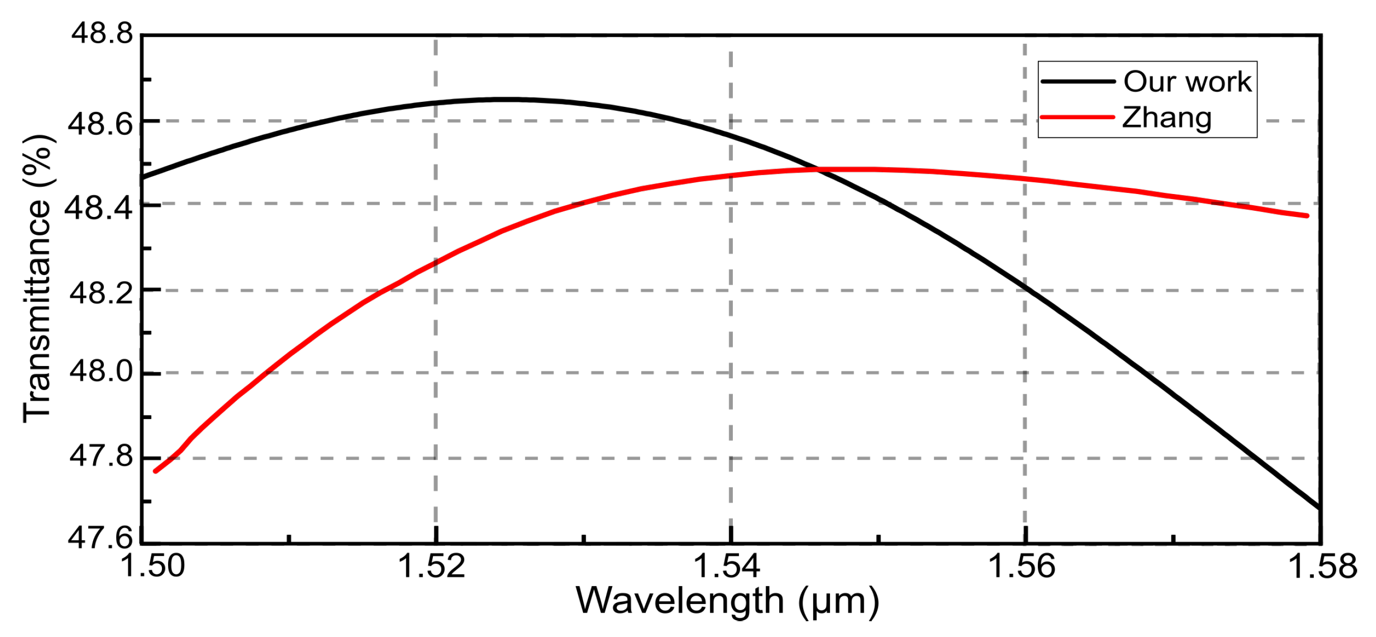
  12. Zhang, Y.; Yang, S.; Lim, A.E.J.; Lo, G.Q.; Galland, C.; Baehr-Jones, T.; Hochberg, M. A compact and low loss Y-junction for submicron silicon waveguide. Opt. Express 2013, 21, 1310–1316. [Google Scholar] [CrossRef]
  13. Piggott, A.Y.; Petykiewicz, J.; Su, L.; Vučković, J. Fabrication-constrained nanophotonic inverse design. Sci. Rep. 2017, 7, 1786. [Google Scholar] [CrossRef] [Green Version]
  14. Lin, Z.; Shi, W. Broadband, low-loss silicon photonic Y-junction with an arbitrary power splitting ratio. Opt. Express 2019, 27, 14338–14343. [Google Scholar] [CrossRef]
  15. Su, L.; Vercruysse, D.; Skarda, J.; Sapra, N.V.; Petykiewicz, J.A.; Vučković, J. Nanophotonic inverse design with SPINS: Software architecture and practical considerations. Appl. Phys. Rev. 2020, 7, 011407. [Google Scholar] [CrossRef]
  16. Kennedy, J.; Eberhart, R. Particle swarm optimization. In Proceedings of the Proceedings of ICNN’95, Perth, WA, Australia, 27 November–1 December 1995; Volume 4, pp. 1942–1948. [Google Scholar] [CrossRef]
  17. Holland, J.H. Adaptation in Natural and Artificial Systems, 2nd ed.; The MIT Press: Cambridge, MA, USA, 1992. [Google Scholar]
  18. Schneider, P.I.; Garcia Santiago, X.; Soltwisch, V.; Hammerschmidt, M.; Burger, S.; Rockstuhl, C. Benchmarking Five Global Optimization Approaches for Nano-optical Shape Optimization and Parameter Reconstruction. ACS Photonics 2019, 6, 2726–2733. [Google Scholar] [CrossRef]
  19. Hansen, N.; Ostermeier, A. Completely derandomized self-adaptation in evolution strategies. Evol. Comput. 2001, 9, 159–195. [Google Scholar] [CrossRef]
  20. Gregory, M.D.; Martin, S.V.; Werner, D.H. Improved Electromagnetics Optimization: The covariance matrix adaptation evolutionary strategy. IEEE Antennas Propag. Mag. 2015, 57, 48–59. [Google Scholar] [CrossRef]
  21. Svanberg, K. The method of moving asymptotes—a new method for structural optimization. Int. J. Numer. Methods Eng. 1987, 24, 359–373. [Google Scholar] [CrossRef]
  22. Byrd, R.H.; Lu, P.; Nocedal, J.; Zhu, C. A Limited Memory Algorithm for Bound Constrained Optimization. SIAM J. Sci. Comput. 1995, 16, 1190–1208. [Google Scholar] [CrossRef]
  23. Storn, R.; Price, K. Differential Evolution—A Simple and Efficient Heuristic for global Optimization over Continuous Spaces. J. Glob. Optim. 1997, 11, 341–359. [Google Scholar] [CrossRef]
  24. Molesky, S.; Lin, Z.; Piggott, A.Y.; Jin, W.; Vucković, J.; Rodriguez, A.W. Inverse design in nanophotonics. Nat. Photonics 2018, 12, 659–670. [Google Scholar] [CrossRef] [Green Version]
  25. Elsawy, M.M.; Lanteri, S.; Duvigneau, R.; Fan, J.A.; Genevet, P. Numerical Optimization Methods for Metasurfaces. Laser Photonics Rev. 2020, 14, 1900445. [Google Scholar] [CrossRef]
  26. De la Cruz-Coronado, J.M.; Prosopio-Galarza, R.; Rubio-Noriega, R.E. Silicon Photonics Foundry-oriented Y-junction Optimization. In Proceedings of the 2020 IEEE XXVII International Conference on Electronics, Electrical Engineering and Computing (INTERCON), Lima, Peru, 3–5 September 2020; pp. 1–4. [Google Scholar] [CrossRef]
  27. Prosopio-Galarza, R.; De La Cruz-Coronado, J.; Hernandez-Figueroa, H.E.; Rubio-Noriega, R. Comparison between optimization techniques for Y-junction devices in SOI substrates. In Proceedings of the 2019 IEEE XXVI International Conference on Electronics, Electrical Engineering and Computing (INTERCON), Lima, Peru, 12–14 August 2019; pp. 1–4. [Google Scholar] [CrossRef]
  28. Mak, J.C.; Sideris, C.; Jeong, J.; Hajimiri, A.; Poon, J.K. Binary particle swarm optimized 2 × 2 power splitters in a standard foundry silicon photonic platform. Opt. Lett. 2016, 41, 3868–3871. [Google Scholar] [CrossRef] [PubMed]
  29. Lu, Q.; Wei, W.; Yan, X.; Shen, B.; Luo, Y.; Zhang, X.; Ren, X. Particle swarm optimized ultra-compact polarization beam splitter on silicon-on-insulator. Photonics Nanostructures-Fundam. Appl. 2018, 32, 19–23. [Google Scholar] [CrossRef]
  30. Xu, J.; Liu, Y.; Guo, X.; Song, Q.; Xu, K. Inverse design of a dual-mode 3-dB optical power splitter with a 445 nm bandwidth. Opt. Express 2022, 30, 26266–26274. [Google Scholar] [CrossRef]
  31. Xu, K.; Liu, L.; Wen, X.; Sun, W.; Zhang, N.; Yi, N.; Sun, S.; Xiao, S.; Song, Q. Integrated photonic power divider with arbitrary power ratios. Opt. Lett. 2017, 42, 855–858. [Google Scholar] [CrossRef] [PubMed]
  32. Wang, Y.; Gao, S.; Wang, K.; Skafidas, E. Ultra-broadband and low-loss 3 dB optical power splitter based on adiabatic tapered silicon waveguides. Opt. Lett. 2016, 41, 2053–2056. [Google Scholar] [CrossRef]
  33. Tahersima, M.H.; Kojima, K.; Koike-Akino, T.; Jha, D.; Wang, B.; Lin, C.; Parsons, K. Deep neural network inverse design of integrated photonic power splitters. Sci. Rep. 2019, 9, 1368. [Google Scholar] [CrossRef]
  34. Ruiz, J.L.P.; Amad, A.A.S.; Gabrielli, L.H.; Novotny, A.A. Optimization of the electromagnetic scattering problem based on the topological derivative method. Opt. Express 2019, 27, 33586–33605. [Google Scholar] [CrossRef]
  35. Ma, Y.; Zhang, Y.; Yang, S.; Novack, A.; Ding, R.; Lim, A.E.J.; Lo, G.Q.; Baehr-Jones, T.; Hochberg, M. Ultralow loss single layer submicron silicon waveguide crossing for SOI optical interconnect. Opt. Express 2013, 21, 29374–29382. [Google Scholar] [CrossRef]
  36. Angulo-Salas, A.; Hernandez-Figueroa, H.E.; Rubio-Noriega, R.E. A new heuristic method For Y-branches using genetic algorithm with optimum dataset generated with particle swarm optimization. In Proceedings of the Silicon Photonics XVI, Online, 6–11 March 2021; Volume 11691, p. 116910Z. [Google Scholar]
  37. Fu, P.H.; Huang, D.W. Optimization of a Polarization Beam Splitter for Broadband Operation using a Genetic Algorithm. In Proceedings of the 2018 IEEE 15th International Conference on Group IV Photonics (GFP), Cancun, Mexico, 29–31 August 2018. [Google Scholar]
  38. Fu, P.H.; Huang, T.Y.; Fan, K.W.; Huang, D.W. Optimization for ultrabroadband polarization beam splitters using a genetic algorithm. IEEE Photonics J. 2018, 11, 6600611. [Google Scholar] [CrossRef]
  39. da Silva Santos, C.H.; Gonçalves, M.S.; Hernández-Figueroa, H.E. Designing Novel Photonic Devices by Bio-Inspired Computing. IEEE Photonics Technol. Lett. 2010, 22, 1177–1179. [Google Scholar] [CrossRef]
  40. Kojima, K.; Koike-Akino, T. Novel multimode interference devices for wavelength beam splitting/combining. In Proceedings of the 2015 International Conference on Photonics in Switching (PS), Florence, Italy, 22–25 September 2015. [Google Scholar]
  41. Baskar, S.; Suganthan, P.; Ngo, N.; Alphones, A.; Zheng, R. Design of triangular FBG filter for sensor applications using covariance matrix adapted evolution algorithm. Opt. Commun. 2006, 260, 716–722. [Google Scholar] [CrossRef]
  42. Hansen, N. The CMA Evolution Strategy: A Tutorial. arXiv 2016, arXiv:1604.00772. [Google Scholar]
  43. Absil, P.P.; De Heyn, P.; Chen, H.; Verheyen, P.; Lepage, G.; Pantouvaki, M.; De Coster, J.; Khanna, A.; Drissi, Y.; Van Thourhout, D.; et al. Imec iSiPP25G silicon photonics: A robust CMOS-based photonics technology platform. In Proceedings of the Silicon Photonics X; SPIE: Bellingham, WA, USA, 2015; Volume 9367, pp. 166–171. [Google Scholar]
Figure 1. Timeline of the optimization methods. Adoption by the number of citations in photonics compared to the total citations (based on Google Scholar results). GA: genetic algorithms; MMA: moving asymptotes; PSO: particle swarm optimization; L-BFGS-B: limited memory Broyden–Fletcher–Goldfarb–Shanno bound constrained; DE: differential evolution; CMA-ES: covariance matrix adaptation evolution strategy.
Photonics 10 00152 g001
Figure 2. Layout of the top view of the splitter. The lengths of the widths W 1 , 2 , 3 , . . . , z were optimized by the angles, α i , which are the parameters of the optimization. The figure of merit (FOM) is the transmittance over a window of frequency taken at the monitor.
Photonics 10 00152 g002
Figure 3. History of the FOM for each algorithm (GA, PSO and CMA-ES) in every optimization process. (Top) SCL band. (Bottom) OESCL band.
Photonics 10 00152 g003
Figure 4. Similarity of the FOM for each algorithm (GA, PSO, and CMA-ES) in every optimization process. (Top) SCL-band. (Bottom) OESCL-band.
Photonics 10 00152 g004
Figure 5. Waveband performance of our work compared with Zhang’s device [12]. Our work shows the best result using CMA-ES.
Photonics 10 00152 g005
Figure 6. Waveband analysis of the best (solid lines) and the worst (dashed lines) executions for each algorithm. (Top) SCL-band and (Bottom) OESCL-band.
Photonics 10 00152 g006
Figure 7. Normalized electric field distributions achieved with the best parameters after the the CMA-ES optimization at the O- and C-bands. Note that at 1330 nm (left), the evanescent field has a smaller magnitude than at 1550 nm (right) resulting in smaller loss at the gap between the two arms.
Photonics 10 00152 g007
Table 1. Comparison of photonic devices designed using iterative optimization algorithms.
WorkDeviceMethodBandwidthLossSize
Mak 2016 [28]2  × 2 splitterPSO1530–1570 nmS: 4.11 dB E: 6 dB4.8 × 4.8 μ m 2
Lu 2018 [29]Beam splitterPSO1500–1600 nmS: no losses2 × 2 μ m 2
Chang 2018 [10]3 dB Y-splitterSubwavelength inverse design1520–1580 nmE: 1.5 dB2.88 × 2.88 μ m 2
Xu 2022 [30]3 dB Y-splitterADTO1588–2033 nmS: 0.83 dB5.4 × 2.88 μ m 2
Xu 2017 [31]3 dB Y-splitterNonlinear fast search1530–1560 nmE: 0.96 dB3.6 × 3.6 μ m 2
Piggott 2017 [13]1 × 3 splitterInverse design1400–1700 nmE: 0.64 dB3.8 × 2.5 μ m 2
Wang 2016 [32]3 dB Y-splitterTaper design1530–1600 nmE: <0.19 dB5 μ m length taper
Tahersima 2019 [33]3 dB Y-splitterDNN inverse design1450–1650 nmS: 0.45 dB2.6 × 2.6 μ m 2
Our work3 dB Y-splitterCMA-ES1260–1625 nmS: 0.15 dB2 × 1.2 μ m 2
Losses (S) means the simulation results whereas response (E) signifies the experimental results. PSO: particle swarm optimization. ADTO: analog and digital topology optimization. DNN: deep neural network.
Table 2. Algorithm’s parameters.
ParameterValueDescription
n40population size
k100number of iterations
p11number of characteristics
q10number of selected parents
r3range of random change in parameters
ω 1inertia weight
c i 1relative attraction coefficients
Disclaimer/Publisher’s Note: The statements, opinions and data contained in all publications are solely those of the individual author(s) and contributor(s) and not of MDPI and/or the editor(s). MDPI and/or the editor(s) disclaim responsibility for any injury to people or property resulting from any ideas, methods, instructions or products referred to in the content.

