Tunable Metasurfaces Based on Mechanically Deformable Polymeric Substrates

 ,
,
Abstract
:1. Introduction
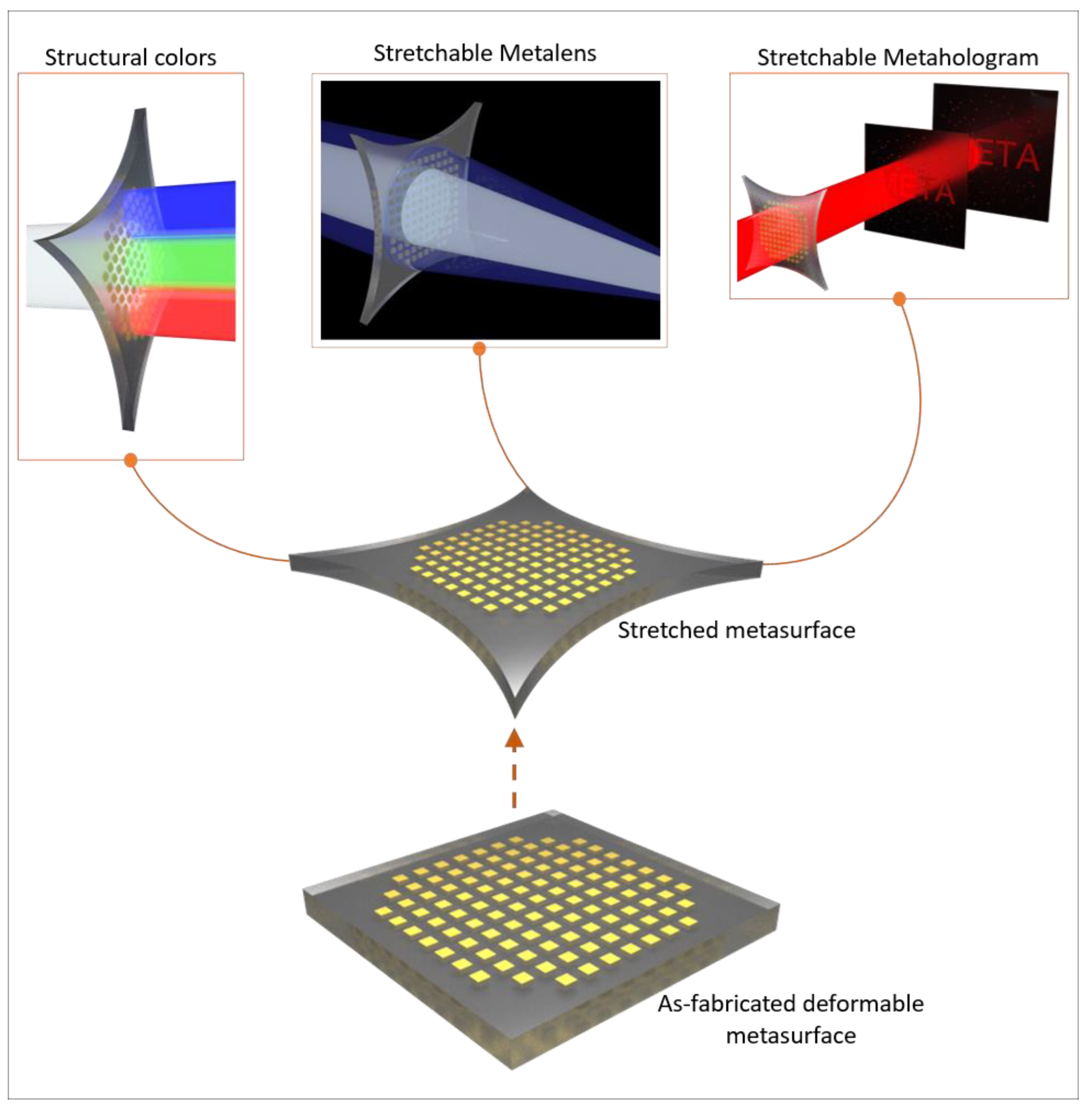
2. Flexible–Deformable Metasurfaces
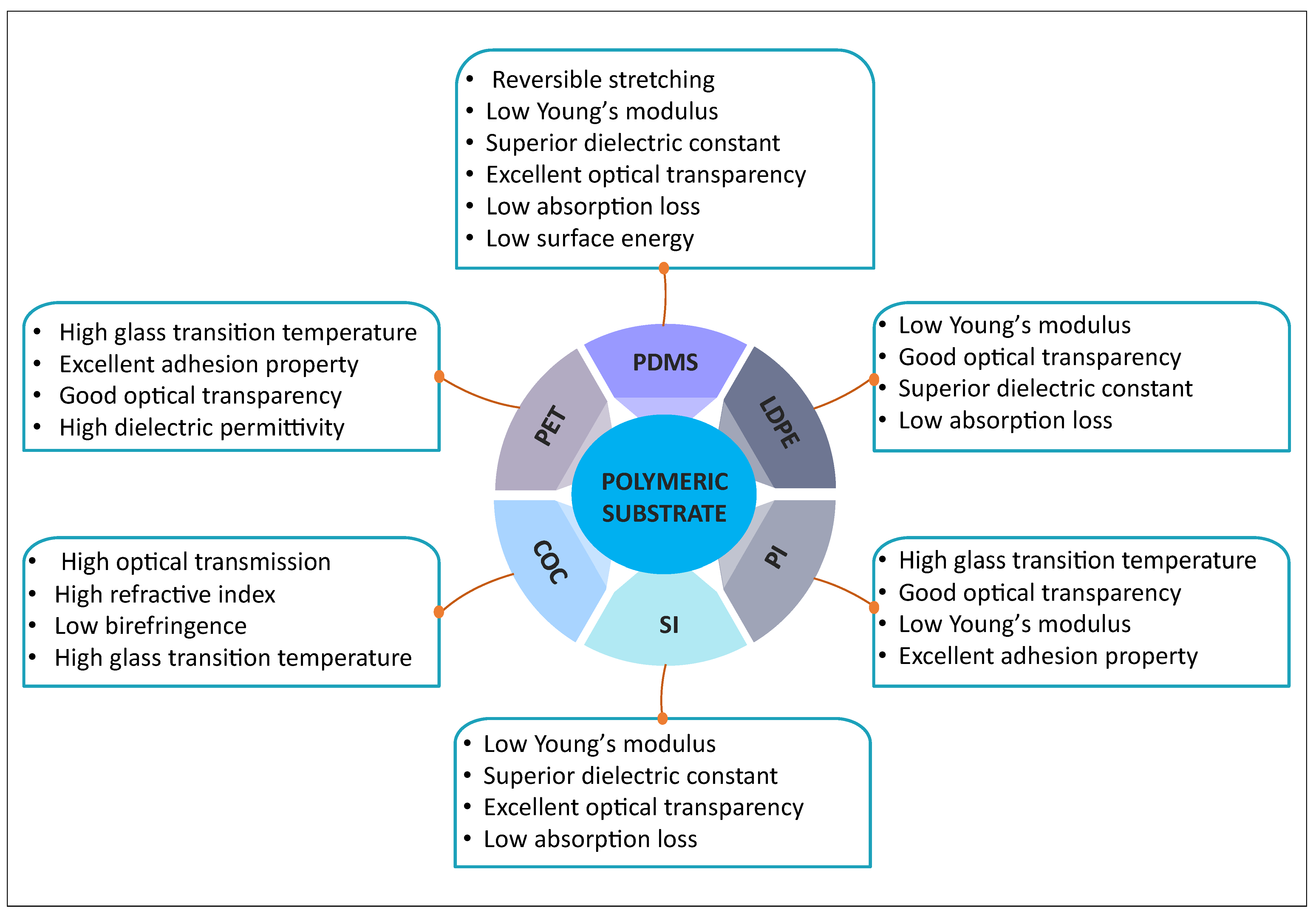
Polymeric Substrates
3. Representative Metasurface Applications
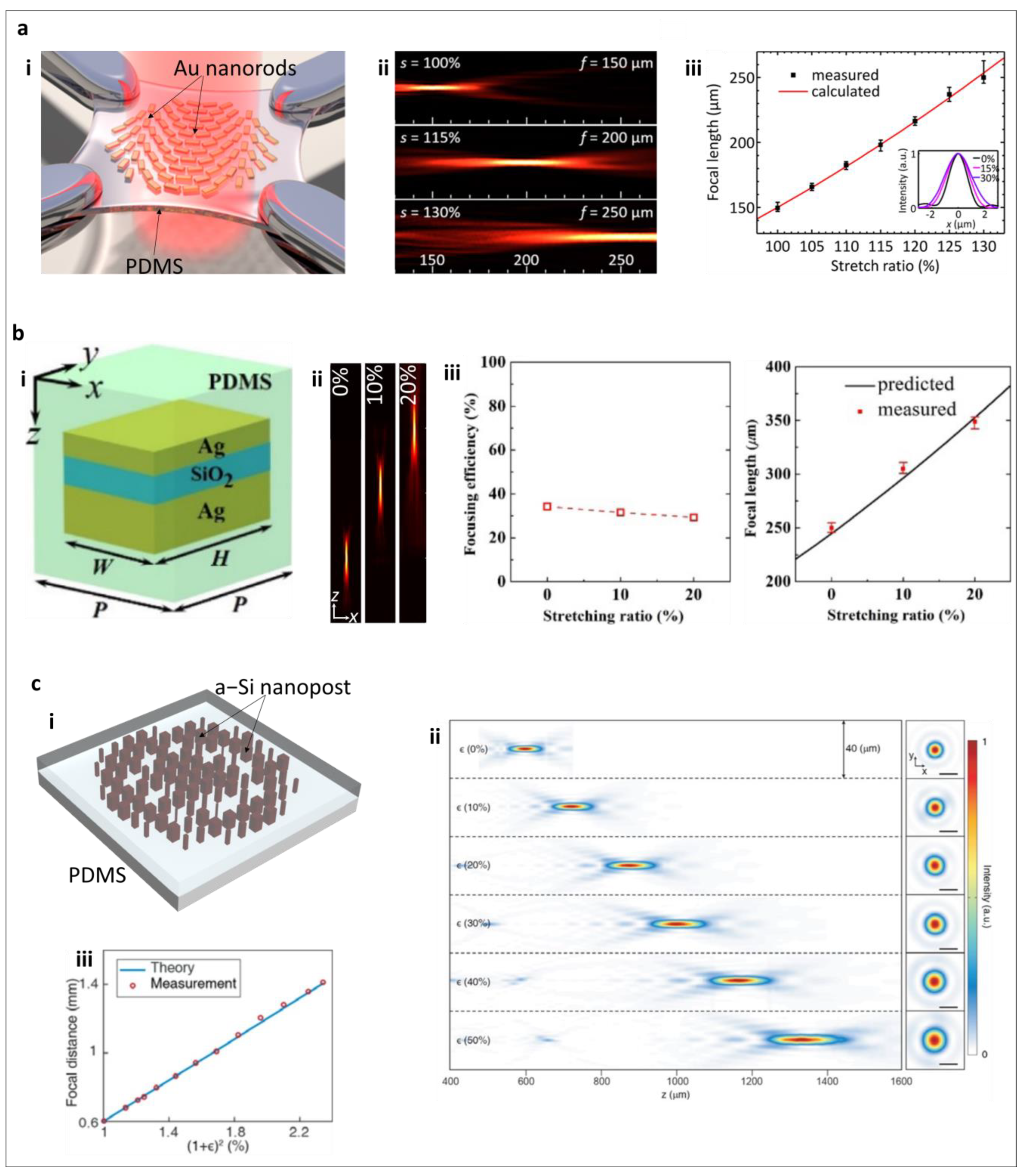
3.1. Stretchable Metalens

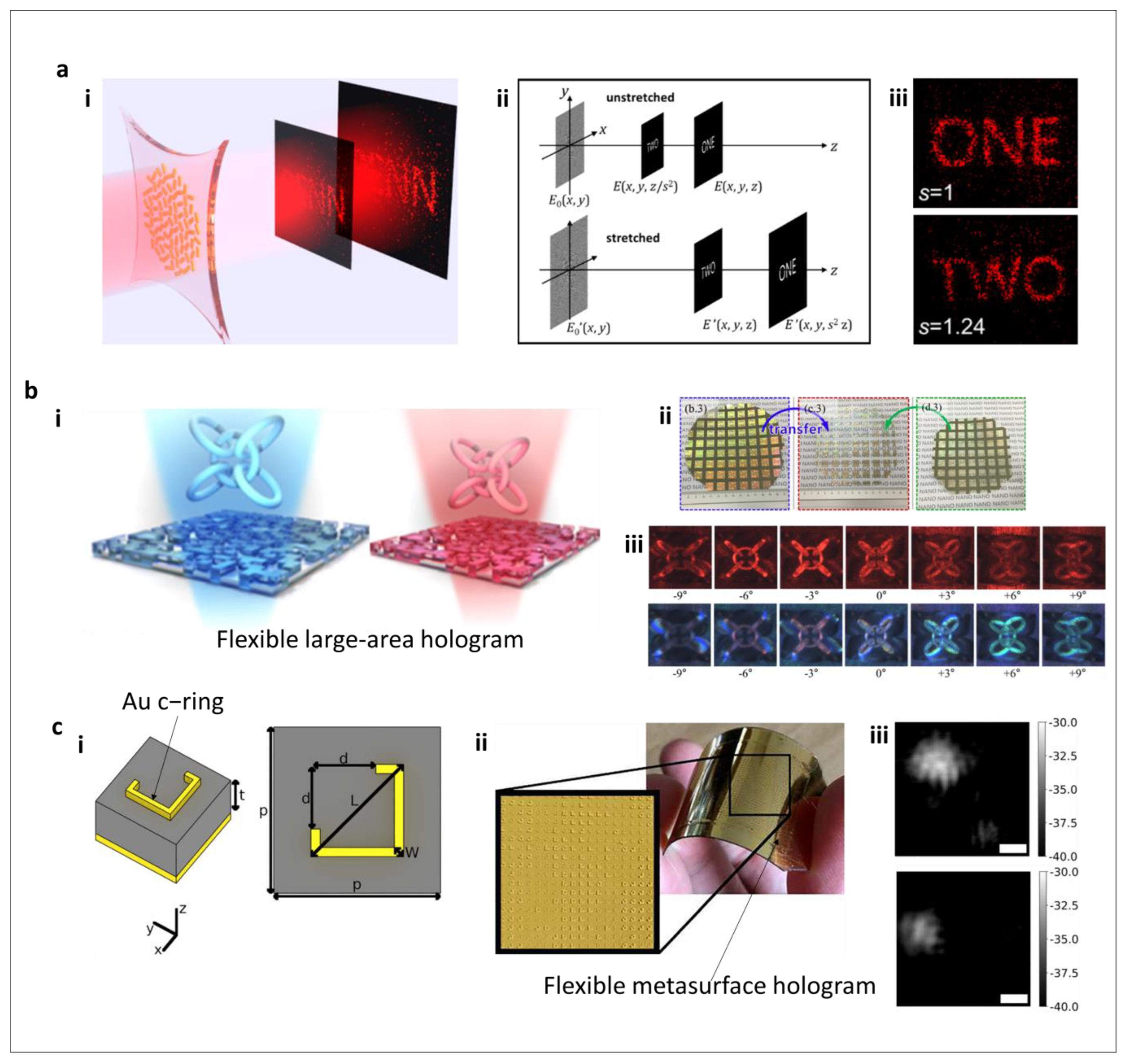
3.2. Stretchable Metahologram
3.3. Plasmonic Resonance
3.4. Structural Color Filters
4. Conclusions and Future Outlook
Author Contributions
Funding
Institutional Review Board Statement
Informed Consent Statement
Data Availability Statement
Conflicts of Interest
References
- Chen, W.T.; Zhu, A.Y.; Khorasaninejad, M.; Shi, Z.; Sanjeev, V.; Capasso, F. Immersion Meta-Lenses at Visible Wavelengths for Nanoscale Imaging. Nano Lett. 2017, 17, 3188–3194. [Google Scholar] [CrossRef] [PubMed]
- Wang, S.; Wu, P.C.; Su, V.-C.; Lai, Y.-C.; Chen, M.K.; Kuo, H.Y.; Chen, B.H.; Chen, Y.H.; Huang, T.-T.; Wang, J.-H.; et al. A broadband achromatic metalens in the visible. Nat. Nanotechnol. 2018, 13, 227–232. [Google Scholar] [CrossRef] [PubMed]
- Chen, L.; Ma, Q.; Nie, Q.F.; Hong, Q.R.; Cui, H.Y.; Ruan, Y.; Cui, T.J. Dual-polarization programmable metasurface modulator for near-field information encoding and transmission. Photon. Res. 2021, 9, 116. [Google Scholar] [CrossRef]
- Chen, Q.; Liu, Y.; Lei, Y.; Pian, S.; Wang, Z.; Ma, Y. Recent Progress on Achromatic Metalenses (Invited Review). Prog. Electromagn. Res. 2022, 173, 9–23. [Google Scholar] [CrossRef]
- Khorasaninejad, M.; Shi, Z.; Zhu, A.Y.; Chen, W.T.; Sanjeev, V.; Zaidi, A.; Capasso, F. Achromatic Metalens over 60 nm Bandwidth in the Visible and Metalens with Reverse Chromatic Dispersion. Nano Lett. 2017, 17, 1819–1824. [Google Scholar] [CrossRef] [Green Version]
- Ou, K.; Yu, F.; Li, G.; Wang, W.; Chen, J.; Miroshnichenko, A.E.; Huang, L.; Li, T.; Li, Z.; Chen, X.; et al. Broadband Achromatic Metalens in Mid-Wavelength Infrared. Laser Photon-Rev. 2021, 15, 2100020. [Google Scholar] [CrossRef]
- Chen, W.T.; Zhu, A.Y.; Sanjeev, V.; Khorasaninejad, M.; Shi, Z.; Lee, E.; Capasso, F. A broadband achromatic metalens for focusing and imaging in the visible. Nat. Nanotechnol. 2018, 13, 220–226. [Google Scholar] [CrossRef] [Green Version]
- Chen, L.; Ma, Q.; Luo, S.S.; Ye, F.J.; Cui, H.Y.; Cui, T.J. Touch-Programmable Metasurface for Various Electromagnetic Manipulations and Encryptions. Small 2022, 18, 2203871. [Google Scholar] [CrossRef]
- Chen, H.-T.; Taylor, A.J.; Yu, N. A review of metasurfaces: Physics and applications. Rep. Prog. Phys. 2016, 79, 076401. [Google Scholar] [CrossRef] [Green Version]
- Engelberg, J.; Levy, U. The advantages of metalenses over diffractive lenses. Nat. Commun. 2020, 11, 1991. [Google Scholar] [CrossRef] [Green Version]
- Ma, Q.; Gao, W.; Xiao, Q.; Ding, L.; Gao, T.; Zhou, Y.; Gao, X.; Yan, T.; Liu, C.; Gu, Z.; et al. Directly wireless communication of human minds via non-invasive brain-computer-metasurface platform. Elight 2022, 2, 1–11. [Google Scholar] [CrossRef]
- Fan, Z.-B.; Qiu, H.-Y.; Zhang, H.-L.; Pang, X.-N.; Zhou, L.-D.; Liu, L.; Ren, H.; Wang, Q.-H.; Dong, J.-W. A broadband achromatic metalens array for integral imaging in the visible. Light. Sci. Appl. 2019, 8, 67. [Google Scholar] [CrossRef] [PubMed] [Green Version]
- Presutti, F.; Monticone, F. Focusing on bandwidth: Achromatic metalens limits. Optica 2020, 7, 624–631. [Google Scholar] [CrossRef]
- Ambhire, S.C.; Palkhivala, S.; Agrawal, A.; Gupta, A.; Rana, G.; Mehta, R.; Bhattacharya, A.; Venugopal, A.; Prabhu, S.S. “Reverse Fabrication” Technique to Develop Mechanically Tunable THz Metasurfaces using a Flexible Polydimethylsiloxane Substrate. In Proceedings of the 43rd International Conference on Infrared, Millimeter, and Terahertz Waves (Irmmw-Thz), Nagoya, Japan, 9–14 September 2018. [Google Scholar] [CrossRef]
- Kim, J.; Seong, J.; Yang, Y.; Moon, S.-W.; Badloe, T.; Rho, J. Tunable metasurfaces towards versatile metalenses and metaholograms: A review. Adv. Photon. 2022, 4, 024001. [Google Scholar] [CrossRef]
- Ullah, N.; Zhao, R.Z.; Huang, L.L. Recent Advancement in Optical Metasurface: Fundament to Application. Micromachines 2022, 13, 1025. [Google Scholar] [CrossRef]
- Ma, Q.; Bai, G.D.; Jing, H.B.; Yang, C.; Li, L.; Cui, T.J. Smart metasurface with self-adaptively reprogrammable functions. Light. Sci. Appl. 2019, 8, 1–12. [Google Scholar] [CrossRef] [Green Version]
- He, Q.; Sun, S.; Zhou, L. Tunable/Reconfigurable Metasurfaces: Physics and Applications. Research 2019, 2019, 1849272. [Google Scholar] [CrossRef] [Green Version]
- Polavarapu, L.; Liz-Marzán, L.M. Towards low-cost flexible substrates for nanoplasmonic sensing. Phys. Chem. Chem. Phys. 2012, 15, 5288–5300. [Google Scholar] [CrossRef]
- Ee, H.-S.; Agarwal, R. Tunable Metasurface and Flat Optical Zoom Lens on a Stretchable Substrate. Nano Lett. 2016, 16, 2818–2823. [Google Scholar] [CrossRef]
- Ahmed, R.; Butt, H. Strain-Multiplex Metalens Array for Tunable Focusing and Imaging. Adv. Sci. 2021, 8, 2003394. [Google Scholar] [CrossRef]
- Walia, S.; Shah, C.M.; Gutruf, P.; Nili, H.; Chowdhury, D.R.; Withayachumnankul, W.; Bhaskaran, M.; Sriram, S. Flexible metasurfaces and metamaterials: A review of materials and fabrication processes at micro- and nano-scales. Appl. Phys. Rev. 2015, 2, 011303. [Google Scholar] [CrossRef]
- Das, B.; Yun, H.S.; Park, N.; Jeong, J.; Kim, D. A Transformative Metasurface Based on Zerogap Embedded Template. Adv. Opt. Mater. 2021, 9, 2164. [Google Scholar] [CrossRef]
- Babu, B.A.; Madhav, B.T.P.; Srilatha, K.; Rao, M.C.; Das, S. A Multiband Frequency Reconfigurable and Bifunctional Metasurface. Int. J. Electron. Lett. 2022, 1–14. [Google Scholar] [CrossRef]
- Resonance Sensor with Metal–Insulator–Metal Nanodisks on PDMS Substrate. Sci. Rep. 2018, 8, 11812. [CrossRef] [PubMed] [Green Version]
- Cataldi, U.; Caputo, R.; Kurylyak, Y.; Klein, G.; Chekini, M.; Umeton, C.; Bürgi, T. Growing gold nanoparticles on a flexible substrate to enable simple mechanical control of their plasmonic coupling. J. Mater. Chem. C 2014, 2, 7927–7933. [Google Scholar] [CrossRef]
- Alsulami, Q.A.; Wageh, S.; Al-Ghamdi, A.A.; Bilal, R.M.H.; Saeed, M.A. A Tunable and Wearable Dual-Band Metamaterial Absorber Based on Polyethylene Terephthalate (PET) Substrate for Sensing Applications. Polymers 2022, 14, 4503. [Google Scholar] [CrossRef]
- Guo, X.; Hang, Y.; Xie, Z.; Wu, C.; Gao, L.; Liu, C. Flexible and wearable 2.45 GHz CPW-fed antenna using inkjet-printing of silver nanoparticles on pet substrate. Microw. Opt. Technol. Lett. 2016, 59, 204–208. [Google Scholar] [CrossRef]
- Zhang, G.; Hang, Y.; Xie, Z.C.; Wu, C.; Gao, L.; Liu, C. Flexible, all-dielectric metasurface fabricated via nanosphere lithography and its applications in sensing. Opt. Express 2017, 25, 22038–22045. [Google Scholar] [CrossRef] [PubMed]
- Xu, X.; Peng, B.; Li, D.; Zhang, J.; Wong, L.M.; Zhang, Q.; Wang, S.; Xiong, Q. Flexible Visible–Infrared Metamaterials and Their Applications in Highly Sensitive Chemical and Biological Sensing. Nano Lett. 2011, 11, 3232–3238. [Google Scholar] [CrossRef]
- Gusev, S.I.; Soboleva, V.Y.; Kublanova, I.L.; Khodzitsky, M.K. Glucose level sensor based on metasurface in THz frequency range. AIP Conf. Proc. 2019, 2098, 020008. [Google Scholar] [CrossRef]
- Aksu, S.; Huang, M.; Artar, A.; Yanik, A.A.; Selvarasah, S.; Dokmeci, M.R.; Altug, H. Flexible Plasmonics on Unconventional and Nonplanar Substrates. Adv. Mater. 2011, 23, 4422. [Google Scholar] [CrossRef]
- Gao, L.; Zhang, Y.; Doshay, S.; Xie, X.; Luo, H.; Shah, D.; Shi, Y.; Xu, S.; Fang, H.; Fan, J.A.; et al. Optics and Nonlinear Buckling Mechanics in Large-Area, Highly Stretchable Arrays of Plasmonic Nanostructures. ACS Nano 2015, 9, 5968–5975. [Google Scholar] [CrossRef] [PubMed]
- Khan, A.; Li, S.; Tang, X.; Li, W.-D. Nanostructure transfer using cyclic olefin copolymer templates fabricated by thermal nanoimprint lithography. J. Vac. Sci. Technol. B 2014, 32, 06FI02. [Google Scholar] [CrossRef] [Green Version]
- Miranda, I.; Souza, A.; Sousa, P.; Ribeiro, J.; Castanheira, E.M.S.; Lima, R.; Minas, G. Properties and Applications of PDMS for Biomedical Engineering: A Review. J. Funct. Biomater. 2021, 13, 2. [Google Scholar] [CrossRef] [PubMed]
- Qi, D.; Zhang, K.; Tian, G.; Jiang, B.; Huang, Y. Stretchable Electronics Based on PDMS Substrates. Adv. Mater. 2020, 33, 2003155. [Google Scholar] [CrossRef] [PubMed]
- Liaw, D.-J.; Wang, K.-L.; Huang, Y.-C.; Lee, K.-R.; Lai, J.-Y.; Ha, C.-S. Advanced polyimide materials: Syntheses, physical properties and applications. Prog. Polym. Sci. 2012, 37, 907–974. [Google Scholar] [CrossRef]
- MacDonald, W.A. Engineered films for display technologies. J. Mater. Chem. 2003, 14, 4–10. [Google Scholar] [CrossRef]
- Faraj, M.G.; Ibrahim, K.; Ali, M.K.M. PET as a plastic substrate for the flexible optoelectronic applications. Opto. Adv. Mater. Commun. 2011, 5, 879–882. [Google Scholar]
- Choi, M.-C.; Kim, Y.; Ha, C.-S. Polymers for flexible displays: From material selection to device applications. Prog. Polym. Sci. 2008, 33, 581–630. [Google Scholar] [CrossRef]
- David, M.; Disnan, D.; Lardschneider, A.; Wacht, D.; Hoang, H.T.; Ramer, G.; Detz, H.; Lendl, B.; Schmid, U.; Strasser, G.; et al. Structure and mid-infrared optical properties of spin-coated polyethylene films developed for integrated photonics applications. Opt. Mater. Express 2022, 12, 2168. [Google Scholar] [CrossRef]
- Kibirkštis, E.; Mayik, V.; Zatserkovna, R.; Vaitasius, K.; Stepanenko, A.; Kandrotaitė-Janutienė, R.; Venytė, I.; Danilovas, P.P. Study of physical and mechanical properties of partially biodegradable LDPE polymeric films and their application for printing and packaging. Polym. Test. 2022, 112, 107646. [Google Scholar] [CrossRef]
- Xu, M.-M.; Huang, G.-Y.; Feng, S.-S.; McShane, G.J.; Stronge, W.J. Static and Dynamic Properties of Semi-Crystalline Polyethylene. Polymers 2016, 8, 77. [Google Scholar] [CrossRef] [PubMed]
- Jordan, J.L.; Rowland, R.L.; Greenhall, J.; Moss, E.K.; Huber, R.C.; Willis, E.C.; Hrubiak, R.; Kenney-Benson, C.; Bartram, B.; Sturtevant, B.T. Elastic properties of polyethylene from high pressure sound speed measurements. Polymer 2020, 212, 123164. [Google Scholar] [CrossRef]
- You, X.; Ako, R.T.; Lee, W.S.L.; Bhaskaran, M.; Sriram, S.; Fumeaux, C.; Withayachumnankul, W. Terahertz transmissive half-wave metasurface with enhanced bandwidth. Opt. Lett. 2021, 46. [Google Scholar] [CrossRef]
- Zhang, S.; Wong, C.L.; Zeng, S.; Bi, R.; Tai, K.; Dholakia, K.; Olivo, M. Metasurfaces for biomedical applications: Imaging and sensing from a nanophotonics perspective. Nanophotonics 2020, 10, 259–293. [Google Scholar] [CrossRef]
- Su, V.-C.; Chu, C.H.; Sun, G.; Tsai, D.P. Advances in optical metasurfaces: Fabrication and applications [Invited]. Opt. Express 2018, 26, 13148–13182. [Google Scholar] [CrossRef]
- Chanda, D.; Shigeta, K.; Gupta, S.; Cain, T.; Carlson, A.; Mihi, A.; Baca, A.J.; Bogart, G.R.; Braun, P.V.; Rogers, J.A. Large-area flexible 3D optical negative index metamaterial formed by nanotransfer printing. Nat. Nanotechnol. 2011, 6, 402–407. [Google Scholar] [CrossRef]
- Qian, Z.; Tian, S.; Zhou, W.; Wang, J.; Guo, H. Broadband achromatic longitudinal bifocal metalens in the visible range based on a single nanofin unit cell. Opt. Express 2022, 30, 11203. [Google Scholar] [CrossRef]
- Tseng, M.L.; Hsiao, H.-H.; Chu, C.H.; Chen, M.K.; Sun, G.; Liu, A.-Q.; Tsai, D.P. Metalenses: Advances and Applications. Adv. Opt. Mater. 2018, 6, 1800554. [Google Scholar] [CrossRef]
- Zaman, A.U.; Song, K.; Lee, D.-G.; Hur, S. A novel approach to Fabry–Pérot-resonance-based lens and demonstrating deep-subwavelength imaging. Sci. Rep. 2020, 10, 10769. [Google Scholar] [CrossRef]
- Luo, X.; Zhang, F.; Pu, M.; Guo, Y.; Li, X.; Ma, X. Recent advances of wide-angle metalenses: Principle, design, and applications. Nanophotonics 2021, 11, 1–20. [Google Scholar] [CrossRef]
- Fan, C.-Y.; Lin, C.-P.; Su, G.-D.J. Ultrawide-angle and high-efficiency metalens in hexagonal arrangement. Sci. Rep. 2020, 10, 15677. [Google Scholar] [CrossRef]
- Ali, F.; Aksu, S. A hybrid broadband metalens operating at ultraviolet frequencies. Sci. Rep. 2021, 11, 2303. [Google Scholar] [CrossRef]
- Chen, M.-H.; Chou, W.-N.; Su, V.-C.; Kuan, C.-H.; Lin, H.Y. High-performance gallium nitride dielectric metalenses for imaging in the visible. Sci. Rep. 2021, 11, 6500. [Google Scholar] [CrossRef] [PubMed]
- Banerji, S.; Meem, M.; Majumder, A.; Vasquez, F.G.; Sensale-Rodriguez, B.; Menon, R. Imaging with flat optics: Metalenses or diffractive lenses? Optica 2019, 6, 805–810. [Google Scholar] [CrossRef]
- Chen, M.-H.; Yen, C.-W.; Guo, C.-C.; Su, V.-C.; Kuan, C.-H.; Lin, H.Y. Polarization-insensitive GaN metalenses at visible wavelengths. Sci. Rep. 2021, 11, 14541. [Google Scholar] [CrossRef] [PubMed]
- Moon, S.-W.; Kim, Y.; Yoon, G.; Rho, J. Recent Progress on Ultrathin Metalenses for Flat Optics. Iscience 2020, 23, 101877. [Google Scholar] [CrossRef] [PubMed]
- Aieta, F.; Genevet, P.; Kats, M.A.; Yu, N.; Blanchard, R.; Gaburro, Z.; Capasso, F. Aberration-Free Ultrathin Flat Lenses and Axicons at Telecom Wavelengths Based on Plasmonic Metasurfaces. Nano Lett. 2012, 12, 4932–4936. [Google Scholar] [CrossRef]
- Yu, N.; Capasso, F. Flat optics with designer metasurfaces. Nat. Mater. 2014, 13, 139–150. [Google Scholar] [CrossRef]
- Aieta, F.; Kats, M.A.; Genevet, P.; Capasso, F. Multiwavelength achromatic metasurfaces by dispersive phase compensation. Science 2015, 347, 1342–1345. [Google Scholar] [CrossRef]
- Fu, X.; Liang, H.; Li, J. Metalenses: From design principles to functional applications. Front. Optoelectron. 2021, 14, 170–186. [Google Scholar] [CrossRef] [PubMed]
- Arbabi, E.; Arbabi, A.; Kamali, S.M.; Horie, Y.; Faraon, A. Multiwavelength polarization-insensitive lenses based on dielectric metasurfaces with meta-molecules. Optica 2016, 3, 628–633. [Google Scholar] [CrossRef] [Green Version]
- Liu, W.; Cheng, H.; Tian, J.; Chen, S. Diffractive metalens: From fundamentals, practical applications to current trends. Adv. Physics: X 2020, 5, 1801477. [Google Scholar] [CrossRef] [Green Version]
- Arbabi, E.; Arbabi, A.; Kamali, S.M.; Horie, Y.; Faraon, A. Multiwavelength metasurfaces through spatial multiplexing. Sci. Rep. 2016, 6, 32803. [Google Scholar] [CrossRef] [Green Version]
- Avayu, O.; Almeida, E.; Prior, Y.; Ellenbogen, T. Composite functional metasurfaces for multispectral achromatic optics. Nat. Commun. 2017, 8, 14992. [Google Scholar] [CrossRef] [Green Version]
- Chen, M.K.; Wu, Y.F.; Fan, Q.B.; Lu, M.G.; Xu, T.; Tsai, D.P. Principles, Functions, and Applications of Optical Meta-Lens. Adv. Opt. Mater. 2021, 9, 2001414. [Google Scholar] [CrossRef]
- Balli, F.; Sultan, M.; Lami, S.K.; Hastings, J.T. A hybrid achromatic metalens. Nat. Commun. 2020, 11, 1–8. [Google Scholar] [CrossRef]
- Lin, R.J.; Su, V.-C.; Wang, S.; Chen, M.K.; Chung, T.L.; Chen, Y.H.; Kuo, H.Y.; Chen, J.-W.; Chen, J.; Huang, Y.-T.; et al. Achromatic metalens array for full-colour light-field imaging. Nat. Nanotechnol. 2019, 14, 227–231. [Google Scholar] [CrossRef]
- McClung, A.; Mansouree, M.; Arbabi, A. At-will chromatic dispersion by prescribing light trajectories with cascaded metasurfaces. Light. Sci. Appl. 2020, 9, 93. [Google Scholar] [CrossRef]
- Shrestha, S.; Overvig, A.C.; Lu, M.; Stein, A.; Yu, N. Broadband achromatic dielectric metalenses. Light. Sci. Appl. 2018, 7, 1–11. [Google Scholar] [CrossRef] [Green Version]
- Zhou, H.; Chen, L.; Shen, F.; Guo, K.; Guo, Z. Broadband Achromatic Metalens in the Midinfrared Range. Phys. Rev. Appl. 2019, 11, 024066. [Google Scholar] [CrossRef]
- Song, N.; Xu, N.; Shan, D.; Zhao, Y.; Gao, J.; Tang, Y.; Sun, Q.; Chen, X.; Wang, Y.; Feng, X. Broadband Achromatic Metasurfaces for Longwave Infrared Applications. Nanomaterials 2021, 11, 2760. [Google Scholar] [CrossRef]
- Xiong, B.; Wang, J.; Peng, R.; Jing, H.; Fan, R.; Qi, D.; Chen, F.; Wang, M. Construct Achromatic Polymer Microlens for High-Transmission Full-Color Imaging. Adv. Opt. Mater. 2020, 9, 1524. [Google Scholar] [CrossRef]
- Cheng, W.; Feng, J.; Wang, Y.; Peng, Z.; Zang, S.; Cheng, H.; Ren, X.; Shuai, Y.; Liu, H.; Wu, J.; et al. Genetic algorithms designed ultra-broadband achromatic metalens in the visible. Optik 2022, 258, 168868. [Google Scholar] [CrossRef]
- Wang, Y.; Chen, Q.; Yang, W.; Ji, Z.; Jin, L.; Ma, X.; Song, Q.; Boltasseva, A.; Han, J.; Shalaev, V.M.; et al. High-efficiency broadband achromatic metalens for near-IR biological imaging window. Nat. Commun. 2021, 12, 1–7. [Google Scholar] [CrossRef]
- Li, Z.; Lin, P.; Huang, Y.-W.; Park, J.-S.; Chen, W.T.; Shi, Z.; Qiu, C.-W.; Cheng, J.-X.; Capasso, F. Meta-optics achieves RGB-achromatic focusing for virtual reality. Sci. Adv. 2021, 7, eabe4458. [Google Scholar] [CrossRef] [PubMed]
- Ndao, A.; Hsu, L.; Ha, J.; Park, J.-H.; Chang-Hasnain, C.; Kanté, B. Octave bandwidth photonic fishnet-achromatic-metalens. Nat. Commun. 2020, 11, 1–6. [Google Scholar] [CrossRef]
- Sisler, J.; Chen, W.T.; Zhu, A.Y.; Capasso, F. Controlling dispersion in multifunctional metasurfaces. APL Photon 2020, 5, 056107. [Google Scholar] [CrossRef]
- Pan, M.Y.; Fu, Y.; Zheng, M.; Chen, H.; Zhang, Y.; Duan, H.; Li, Q.; Qiu, M.; Hu, Y. Dielectric metalens for miniaturized imaging systems: Progress and challenges. Light Sci. Appl. 2022, 11, 1–32. [Google Scholar] [CrossRef]
- Li, K.; Pu, G.Y.H.; Pu, M.B.; Li, X.; Ma, X.L.; Zhao, Z.; Luo, X.G. Dispersion controlling meta-lens at visible frequency. Opt. Express 2017, 25, 21419–21427. [Google Scholar]
- Chen, W.T.; Zhu, A.Y.; Capasso, F. Flat optics with dispersion-engineered metasurfaces. Nat. Rev. Mater. 2020, 5, 604–620. [Google Scholar] [CrossRef]
- Li, D.; Wang, X.; Ling, J.; Yuan, Y. Multiwavelength achromatic microlens through phase compensation based on the subwavelength metallic nanostructures. Opt. Commun. 2019, 445, 90–95. [Google Scholar] [CrossRef]
- He, Y.; Song, B.; Tang, J. Optical metalenses: Fundamentals, dispersion manipulation, and applications. Front. Optoelectron. 2022, 15, 1–31. [Google Scholar] [CrossRef] [PubMed]
- Khorasaninejad, M.; Chen, W.T.; Devlin, R.C.; Oh, J.; Zhu, A.Y.; Capasso, F. Metalenses at visible wavelengths: Diffraction-limited focusing and subwavelength resolution imaging. Science 2016, 352, 1190–1194. [Google Scholar] [CrossRef] [PubMed] [Green Version]
- Aiello, M.D.; Backer, A.S.; Sapon, A.J.; Smits, J.; Perreault, J.D.; Llull, P.; Acosta, V.M. Achromatic Varifocal Metalens for the Visible Spectrum. ACS Photon 2019, 6, 2432–2440. [Google Scholar] [CrossRef] [Green Version]
- Zheng, G.; Wu, W.; Li, Z.; Zhang, S.; Mehmood, M.Q.; He, P.; Li, S. Dual field-of-view step-zoom metalens. Opt. Lett. 2017, 42, 1261–1264. [Google Scholar] [CrossRef] [Green Version]
- Liu, W.; Hu, B.; Huang, Z.; Guan, H.; Li, H.; Wang, X.; Zhang, Y.; Yin, H.; Xiong, X.; Liu, J.; et al. Graphene-enabled electrically controlled terahertz meta-lens. Photon Res. 2018, 6, 703–708. [Google Scholar] [CrossRef] [Green Version]
- Zhang, Y.; Lin, C.; Lin, J.; Zeng, X.; Yan, Q.; Zhou, X.; Guo, T. Dual-layer electrode-driven liquid crystal lens with electrically tunable focal length and focal plane. Opt. Commun. 2018, 412, 114–120. [Google Scholar] [CrossRef]
- Badloe, T.; Kim, I.; Kim, Y.; Kim, J.; Rho, J. Electrically Tunable Bifocal Metalens with Diffraction-Limited Focusing and Imaging at Visible Wavelengths. Adv. Sci. 2021, 8, 2102646. [Google Scholar] [CrossRef]
- Fan, C.-Y.; Chuang, T.-J.; Wu, K.-H.; Su, G.-D.J. Electrically modulated varifocal metalens combined with twisted nematic liquid crystals. Opt. Express 2020, 28, 10609–10617. [Google Scholar] [CrossRef]
- Shen, Z.; Zhou, S.; Li, X.; Ge, S.; Chen, P.; Hu, W.; Lu, Y. Liquid crystal integrated metalens with tunable chromatic aberration. Adv. Photon 2020, 2, 036002. [Google Scholar] [CrossRef]
- Berto, P.; Philippet, L.; Osmond, J.; Liu, C.F.; Afridi, A.; Marques, M.M.; Agudo, B.M.; Tessier, G.; Quidant, R. Tunable and free-form planar optics. Nat. Photon 2019, 13, 649–656. [Google Scholar] [CrossRef] [Green Version]
- She, A.; Zhang, S.; Shian, S.; Clarke, D.R.; Capasso, F. Adaptive metalenses with simultaneous electrical control of focal length, astigmatism, and shift. Sci. Adv. 2018, 4, eaap9957. [Google Scholar] [CrossRef] [PubMed] [Green Version]
- Kamali, S.M.; Arbabi, E.; Arbabi, A.; Horie, Y.; Faraon, A. Highly tunable elastic dielectric metasurface lenses. Laser Photon-Rev. 2016, 10, 1002–1008. [Google Scholar] [CrossRef] [Green Version]
- Cheng, F.; Qiu, L.; Nikolov, D.; Bauer, A.; Rolland, J.P.; Vamivakas, A.N. Mechanically tunable focusing metamirror in the visible. Opt. Express 2019, 27, 15194–15204. [Google Scholar] [CrossRef] [PubMed]
- Cathey, W.T., Jr. Spatial Phase Modulation of Wavefronts in Spatial Filtering and Holography. J. Opt. Soc. Am. 1966, 56, 1167–1169. [Google Scholar] [CrossRef]
- Chen, S.; Li, Z.; Zhang, Y.; Cheng, H.; Tian, J. Phase Manipulation of Electromagnetic Waves with Metasurfaces and Its Applications in Nanophotonics. Adv. Opt. Mater. 2018, 6, 1800104. [Google Scholar] [CrossRef]
- Li, X.; Chen, L.; Li, Y.; Zhang, X.; Pu, M.; Zhao, Z.; Ma, X.; Wang, Y.; Hong, M.; Luo, X. Multicolor 3D meta-holography by broadband plasmonic modulation. Sci. Adv. 2016, 2, 1601102. [Google Scholar] [CrossRef] [Green Version]
- Zheng, G.; Mühlenbernd, H.; Kenney, M.; Li, G.; Zentgraf, T.; Zhang, S. Metasurface holograms reaching 80% efficiency. Nat. Nanotechnol. 2015, 10, 308–312. [Google Scholar] [CrossRef]
- Yang, G.-Z.; Dong, B.-Z.; Gu, B.-Y.; Zhuang, J.-Y.; Ersoy, O.K. Gerchberg–Saxton and Yang–Gu algorithms for phase retrieval in a nonunitary transform system: A comparison. Appl. Opt. 1994, 33, 209–218. [Google Scholar] [CrossRef]
- Slinger, C.; Cameron, C.; Stanley, M. Computer-generated holography as a generic display technology. Computer 2005, 38, 46–53. [Google Scholar] [CrossRef]
- Lesem, L.B.; Hirsch, P.M.; Jordan, J.A. Scientific Applications: Computer synthesis of Holograms for 3-D display. Commun. ACM 1968, 11, 661–674. [Google Scholar] [CrossRef]
- Fienup, J.R. Phase retrieval algorithms: A comparison. Appl. Opt. 1982, 21, 2758–2769. [Google Scholar] [CrossRef] [PubMed] [Green Version]
- Ren, H.; Briere, G.; Fang, X.; Ni, P.; Sawant, R.; Héron, S.; Chenot, S.; Vézian, S.; Damilano, B.; Brändli, V.; et al. Metasurface orbital angular momentum holography. Nat. Commun. 2019, 10, 1–8. [Google Scholar] [CrossRef] [PubMed] [Green Version]
- Wen, D.; Yue, F.; Li, G.; Zheng, G.; Chan, K.; Chen, S.; Chen, M.; Li, K.F.; Wong, P.W.H.; Cheah, K.W.; et al. Helicity multiplexed broadband metasurface holograms. Nat. Commun. 2015, 6, 8241. [Google Scholar] [CrossRef] [PubMed] [Green Version]
- Wang, B.; Dong, F.; Yang, D.; Song, Z.; Xu, L.; Chu, W.; Gong, Q.; Li, Y. Polarization-controlled color-tunable holograms with dielectric metasurfaces. Optica 2017, 4, 1368–1371. [Google Scholar] [CrossRef]
- Deng, Z.-L.; Deng, J.; Zhuang, X.; Wang, S.; Li, K.; Wang, Y.; Chi, Y.; Ye, X.; Xu, J.; Wang, G.P.; et al. Diatomic Metasurface for Vectorial Holography. Nano Lett. 2018, 18, 2885–2892. [Google Scholar] [CrossRef]
- Hu, Y.; Ou, X.; Zeng, T.; Lai, J.; Zhang, J.; Li, X.; Luo, X.; Li, L.; Fan, F.; Duan, H. Electrically Tunable Multifunctional Polarization-Dependent Metasurfaces Integrated with Liquid Crystals in the Visible Region. Nano Lett. 2021, 21, 4554–4562. [Google Scholar] [CrossRef]
- Kim, I.; Jang, J.H.; Kim, G.T.; Lee, J.H.; Badloe, T.; Mun, J.H.; Rho, J. S Pixelated bifunctional metasurface-driven dynamic vectorial holographic color prints for photonic security platform. Nat. Commun. 2021, 12, 1–9. [Google Scholar] [CrossRef]
- Cui, T.J.; Qi, M.Q.; Wan, X.; Zhao, J.; Cheng, Q. Coding metamaterials, digital metamaterials and programmable metamaterials. Light. Sci. Appl. 2014, 3, e218. [Google Scholar] [CrossRef] [Green Version]
- Qu, G.; Yang, W.; Song, Q.; Liu, Y.; Qiu, C.-W.; Han, J.; Tsai, D.-P.; Xiao, S. Reprogrammable meta-hologram for optical encryption. Nat. Commun. 2020, 11, 1–5. [Google Scholar] [CrossRef]
- Ma, Q.; Cui, T.J. Information Metamaterials: Bridging the physical world and digital world. Photonix 2020, 1, 1–32. [Google Scholar] [CrossRef] [Green Version]
- Malek, S.C.; Ee, H.-S.; Agarwal, R. Strain Multiplexed Metasurface Holograms on a Stretchable Substrate. Nano Lett. 2017, 17, 3641–3645. [Google Scholar] [CrossRef] [Green Version]
- Kim, M.K. Principles and techniques of digital holographic microscopy. SPIE Rev. 2010, 1, 018005. [Google Scholar] [CrossRef] [Green Version]
- Zhao, Z.-J.; Hwang, S.H.; Kang, H.-J.; Jeon, S.; Bok, M.; Ahn, S.; Im, D.; Hahn, J.; Kim, H.; Jeong, J.-H. Adhesive-Layer-Free and Double-Faced Nanotransfer Lithography for a Flexible Large-Area MetaSurface Hologram. ACS Appl. Mater. Interfaces 2019, 12, 1737–1745. [Google Scholar] [CrossRef]
- Burch, J.; Ma, J.; Hunter, R.I.; Schulz, S.A.; Robertson, D.A.; Smith, G.M.; Wang, J.; Di Falco, A. Flexible patches for mm-wave holography. Appl. Phys. Lett. 2019, 115, 021104. [Google Scholar] [CrossRef] [Green Version]
- Guo, X.; Pu, M.; Guo, Y.; Ma, X.; Li, X.; Luo, X. Flexible and Tunable Dielectric Color Meta-hologram. Plasmonics 2019, 15, 217–223. [Google Scholar] [CrossRef]
- Aravind, P.K. A simple proof of Pancharatnam’s theorem. Opt. Commun. 1992, 94, 191–196. [Google Scholar] [CrossRef]
- Kravets, V.G.; Kabashin, A.V.; Barnes, W.L.; Grigorenko, A.N. Plasmonic Surface Lattice Resonances: A Review of Properties and Applications. Chem. Rev. 2018, 118, 5912–5951. [Google Scholar] [CrossRef] [PubMed]
- Yu, H.; Peng, Y.; Yang, Y.; Li, Z.-Y. Plasmon-enhanced light–matter interactions and applications. npj Comput. Mater. 2019, 5, 45. [Google Scholar] [CrossRef] [Green Version]
- Lin, Y.-S.; Xu, Z. Reconfigurable metamaterials for optoelectronic applications. Int. J. Optomechatronics 2020, 14, 78–93. [Google Scholar] [CrossRef]
- Pryce, I.M.; Aydin, K.; Kelaita, Y.A.; Briggs, R.M.; Atwater, H.A. Highly Strained Compliant Optical Metamaterials with Large Frequency Tunability. Nano Lett. 2010, 10, 4222–4227. [Google Scholar] [CrossRef] [PubMed] [Green Version]
- Huang, F.; Baumberg, J.J. Actively Tuned Plasmons on Elastomerically Driven Au Nanoparticle Dimers. Nano Lett. 2010, 10, 1787–1792. [Google Scholar] [CrossRef] [PubMed]
- Pryce, I.M.; Kelaita, Y.A.; Aydin, K.; Atwater, H.A. Compliant Metamaterials for Resonantly Enhanced Infrared Absorption Spectroscopy and Refractive Index Sensing. ACS Nano 2011, 5, 8167–8174. [Google Scholar] [CrossRef]
- Gutruf, P.; Zou, C.; Withayachumnankul, W.; Bhaskaran, M.; Sriram, S.; Fumeaux, C. Mechanically Tunable Dielectric Resonator Metasurfaces at Visible Frequencies. ACS Nano 2015, 10, 133–141. [Google Scholar] [CrossRef] [Green Version]
- Chen, W.; Liu, W.; Jiang, Y.; Zhang, M.; Song, N.; Greybush, N.J.; Guo, J.; Estep, A.K.; Turner, K.T.; Agarwal, R. Ultrasensitive, Mechanically Responsive Optical Metasurfaces via Strain Amplification. ACS Nano 2018, 12, 10683–10692. [Google Scholar] [CrossRef]
- Chen, F.; Liu, X.; Tian, Y.; Zheng, Y. Mechanically stretchable metamaterial with tunable mid-infrared optical properties. Opt. Express 2021, 29, 37368. [Google Scholar] [CrossRef] [PubMed]
- Chen, Y.; Li, H.; Li, M. Flexible and tunable silicon photonic circuits on plastic substrates. Sci. Rep. 2012, 2, 622. [Google Scholar] [CrossRef] [Green Version]
- Liu, W.; Shen, Y.; Xiao, G.; She, X.; Wang, J.; Jin, C. Mechanically tunable sub-10 nm metal gap by stretching PDMS substrate. Nanotechnology 2017, 28, 075301. [Google Scholar] [CrossRef]
- Liu, X.; Huang, Z.; Zhu, C.; Wang, L.; Zang, J. Out-of-Plane Designed Soft Metasurface for Tunable Surface Plasmon Polariton. Nano Lett. 2018, 18, 1435–1441. [Google Scholar] [CrossRef]
- Yang, A.; Hryn, A.J.; Bourgeois, M.R.; Odom, T.W. Programmable and reversible plasmon mode engineering. Proc. Natl. Acad. Sci. USA 2016, 113, 14201–14206. [Google Scholar] [CrossRef] [Green Version]
- Yu, J.; Liu, Z.; Wang, M.; Wang, C.; Chen, G.; Cui, Z.; Wang, T.; Yang, H.; Wang, X.; Chen, X. Strain-Enabled Phase Transition of Periodic Metasurfaces. Adv. Mater. 2021, 34, 2102560. [Google Scholar] [CrossRef]
- Wang, D.; Bourgeois, M.R.; Lee, W.-K.; Li, R.; Trivedi, D.; Knudson, M.P.; Wang, W.; Schatz, G.C.; Odom, T.W. Stretchable Nanolasing from Hybrid Quadrupole Plasmons. Nano Lett. 2018, 18, 4549–4555. [Google Scholar] [CrossRef]
- Yoo, D.; Johnson, T.W.; Cherukulappurath, S.; Norris, D.J.; Oh, S.-H. Template-Stripped Tunable Plasmonic Devices on Stretchable and Rollable Substrates. ACS Nano 2015, 9, 10647–10654. [Google Scholar] [CrossRef]
- Zhang, C.; Jing, J.; Wu, Y.; Fan, Y.; Yang, W.; Wang, S.; Song, Q.; Xiao, S. Stretchable All-Dielectric Metasurfaces with Polarization-Insensitive and Full-Spectrum Response. ACS Nano 2019, 14, 1418–1426. [Google Scholar] [CrossRef]
- Tseng, M.L.; Yang, J.; Semmlinger, M.; Zhang, C.; Nordlander, P.; Halas, N.J. Two-Dimensional Active Tuning of an Aluminum Plasmonic Array for Full-Spectrum Response. Nano Lett. 2017, 17, 6034–6039. [Google Scholar] [CrossRef]
- Yang, B.; Liu, W.; Choi, D.; Li, Z.; Cheng, H.; Tian, J.; Chen, S. High-Performance Transmission Structural Colors Generated by Hybrid Metal-Dielectric Metasurfaces. Adv. Opt. Mater. 2021, 9, 2100895. [Google Scholar] [CrossRef]
- Fang, B.; Yang, C.; Shen, W.; Zhang, X.; Zhang, Y.; Liu, X. Highly efficient omnidirectional structural color tuning method based on dielectric–metal–dielectric structure. Appl. Opt. 2016, 56, C175–C180. [Google Scholar] [CrossRef]
- Oliveira, I.A.; de Souza, I.L.G.; Rodriguez-Esquerre, V.F. Design of hybrid narrow-band plasmonic absorber based on chalcogenide phase change material in the infrared spectrum. Sci. Rep. 2021, 11, 21912. [Google Scholar] [CrossRef]
- Song, S.; Ma, X.; Pu, M.; Li, X.; Liu, K.; Gao, P.; Zhao, Z.; Wang, Y.; Wang, C.; Luo, X. Actively Tunable Structural Color Rendering with Tensile Substrate. Adv. Opt. Mater. 2017, 5, 1600829. [Google Scholar] [CrossRef]
- Kim, Y.J.; Yoo, Y.J.; Kang, M.H.; Ko, J.H.; Park, M.R.; Yoo, D.E.; Lee, D.W.; Kim, K.; Kang, I.-S.; Song, Y.M. Mechanotunable optical filters based on stretchable silicon nanowire arrays. Nanophotonics 2020, 9, 3287–3293. [Google Scholar] [CrossRef] [Green Version]
- Agata, K.; Murai, S.; Tanaka, K. Stick-and-play metasurfaces for directional light outcoupling. Appl. Phys. Lett. 2021, 118, 021110. [Google Scholar] [CrossRef]
- Wei, S.; Cao, G.; Lin, H.; Yuan, X.; Somekh, M.; Jia, B. A Varifocal Graphene Metalens for Broadband Zoom Imaging Covering the Entire Visible Region. ACS Nano 2021, 15, 4769–4776. [Google Scholar] [CrossRef]
- Ee, H.-S.; Park, H.-G. Design of tunable silicon metasurfaces with cross-polarization transmittance over 80%. Phys. Scr. 2018, 93, 085501. [Google Scholar] [CrossRef]
- Li, J.; Fan, H.; Ye, H.; Wu, T.; Sun, Y.; Wang, X.; Liu, Y. Design of Multifunctional Tunable Metasurface Assisted by Elastic Substrate. Nanomaterials 2022, 12, 2387. [Google Scholar] [CrossRef] [PubMed]
- Kamali, S.M.; Arbabi, A.; Arbabi, E.; Horie, Y.; Faraon, A. Decoupling optical function and geometrical form using conformal flexible dielectric metasurfaces. Nat. Commun. 2016, 7, 11618. [Google Scholar] [CrossRef] [PubMed] [Green Version]
- Kang, H.; Heo, C.-J.; Jeon, H.C.; Lee, S.Y.; Yang, S.-M. Durable Plasmonic Cap Arrays on Flexible Substrate with Real-Time Optical Tunability for High-Fidelity SERS Devices. ACS Appl. Mater. Interfaces 2013, 5, 4569–4574. [Google Scholar] [CrossRef]
- Lee, J.-E.; Park, C.; Chung, K.; Lim, J.W.; Mota, F.M.; Jeong, U.; Kim, D.H. Viable stretchable plasmonics based on unidirectional nanoprisms. Nanoscale 2018, 10, 4105–4112. [Google Scholar] [CrossRef] [PubMed] [Green Version]
- Ambhire, S.C.; Palkhivala, S.; Agrawal, A.; Gupta, A.; Rana, G.; Mehta, R.; Ghindani, D.; Bhattacharya, A.; Achanta, V.G.; Prabhu, S.S. “Pattern and Peel” method for fabricating mechanically tunable terahertz metasurface on an elastomeric substrate. Opt. Mater. Express 2018, 8, 3382–3391. [Google Scholar] [CrossRef]
- Liu, C.; Cai, J.; Li, X.; Zhang, W.; Zhang, D. Flexible and tunable electromagnetic meta-atom based on silver nanowire networks. Mater. Des. 2019, 181, 107982. [Google Scholar] [CrossRef]
- Visser, D.; Basuvalingam, S.B.; Désières, Y.; Anand, S. Optical properties and fabrication of dielectric metasurfaces based on amorphous silicon nanodisk arrays. Opt. Express 2019, 27, 5353–5367. [Google Scholar] [CrossRef] [PubMed] [Green Version]
- Wang, X.; Chen, J.; Guo, T.; Shi, Y. Polarization tunable color filters based on all-dielectric metasurfaces on a flexible substrate. Opt. Express 2020, 28, 21704–21712. [Google Scholar] [CrossRef] [PubMed]
- Lin, H.-T.; Hsu, Y.-Y.; Cheng, P.-J.; Wang, W.-T.; Chang, S.-W.; Shih, M.-H. In situ tunable circular dichroism of flexible chiral metasurfaces composed of plasmonic nanorod trimers. Nanoscale Adv. 2022, 4, 2428–2434. [Google Scholar] [CrossRef]
- Kim, D.; Yun, H.S.; Das, B.; Rhie, J.; Vasa, P.; Kim, Y.-I.; Choa, S.-H.; Park, N.; Lee, D.; Bahk, Y.-M.; et al. Topology-Changing Broadband Metamaterials Enabled by Closable Nanotrenches. Nano Lett. 2021, 21, 4202–4208. [Google Scholar] [CrossRef]
- Lee, Y.-J.; Yeh, T.-W.; Nagarjuna, P.; Tseng, C.-C.; Yi, J.-Y. A strain-gauge random laser. APL Mater. 2019, 7, 061103. [Google Scholar] [CrossRef] [Green Version]
- Hou, G.; Wang, Z.; Lu, Z.; Song, H.; Xu, J.; Chen, K. Enhanced Broadband Plasmonic Absorbers with Tunable Light Management on Flexible Tapered Metasurface. ACS Appl. Mater. Interfaces 2020, 12, 56178–56185. [Google Scholar] [CrossRef] [PubMed]
- Fan, X.; Li, Y.; Chen, S.; Xing, Y.; Pan, T. Mechanical Terahertz Modulation by Skin-Like Ultrathin Stretchable Metasurface. Small 2020, 16, 2002484. [Google Scholar] [CrossRef]


| Polymeric Material | Refractive Index | Young’s Modulus E [MPa] | Dielectric Permittivity [THz] | Operating Temperature [°C] | Optical Transparency [400–800 nm, %] | Elastic Limit [%] | Reference |
|---|---|---|---|---|---|---|---|
| PDMS | 1.4 | 0.36–0.87 | 2.3–2.8 | −45–200 | 74–90% | 200 | [22,35,36] |
| Polyimide | 1.50 | 1.5–3 | 3.24 | 440 | – | 2–15 | [22,37,38] |
| PET | 1.66 | 4–5.3 | 2.86 | 300 | 85–90.4% | – | [38,39,40] |
| LDPE | 1.5 | 8.70–1370 | 2.2–2.4 | 456.2 | – | 79 | [41,42,43,44] |
| COC | 1.51–1.53 | 2600 | 2.33 | – | 94.5% | – | [34,40,45] |
| Substrate for Metasurface | Representative Application | Specific Functionality | Active Material | Stretchability | Tunable Property | Year |
|---|---|---|---|---|---|---|
| Polydimethylsiloxane (PDMS) | Metalens | Flat zoom lens [20] | Gold (Au) nanorod | 30% strain | Focal length 150–250 µm, Operating wavelength 632.8 nm | 2016 |
| Zoom imaging metalens [144] | Graphene oxide film | 10% strain | Focal length 212–376 µm, 450–650 nm | 2021 | ||
| Microlens [95] | Silicon nano-post on thin aluminum oxide | 0–50% strain | Focal length 600–1400 µm, Operating wavelength 915 nm | 2016 | ||
| Reflecting metalens [96] | Silver (Ag)—Silica (SiO2)—Silver (Ag) resonators | 0–20% uniaxial strain | Focal length 250–350 µm Operating wavelength 670 nm | 2019 | ||
| Metalens [128] | Alumina nanopillars | – | average tuning range 109. 2 µm | 2021 | ||
| Flat zoom lens [145] | Crystalline silicon nanoposts | 137% strain | Focal length 320–440 nm, Operating wavelength 680 nm | 2018 | ||
| Beam splitter, reflective mirror [146] | Silicon nanoblock-thin alumina | 0–70% uniaxial strain | 500–580 nm, 532 nm | 2022 | ||
| Polydimethylsiloxane (PDMS) | Metalens | Conformal optics [147] | Silicon nano-post on thin aluminum oxide | – | Operating wavelength 915 nm | 2016 |
| Metahologram | Image switching [114] | Gold nanorod | 0–24% strain | Focal length 150–232 µm | 2017 | |
| Color metahologram [118] | TiO2 nanopoles | – | – | 2020 | ||
| Resonance modulation | Mechano-sensitive plasmonic resonator [127] | Tapered gold microrods-gold gratings | 1.6–3.5% uniaxial strain | Resonance wavelength 744 nm–836 nm | 2018 | |
| Resonance tuning [130] | Gold nanogaps | 100% uniaxial strain | Resonance wavelength red shift | 2017 | ||
| Flexible photonics [129] | Gold micro-ring resonators | 9% uniaxial strain | Resonance wavelength 0.2 nm shift | 2012 | ||
| Tunable Surface-Enhanced Raman Spectroscopy [148] | Silica-gold nanoparticles | 0–30% uniaxial strain | 581–625 nm | 2013 | ||
| Resonance frequency tuning [125] | Gold split ring resonators | 25% uniaxial strain | Resonance frequency 5.78–6.27 µm shift | 2011 | ||
| Dynamic polarization control, birefringence tuning [133] | Gold nanodisks | 0–30% axial strain | Resonance wavelength red shift | 2022 | ||
| Nanolasing [134] | Gold nano particles | 0–5% strain | Resonance wavelength 35 nm shift | 2018 | ||
| Polydimethylsiloxane (PDMS) | Resonance modulation | Surface-Enhanced Raman Spectroscopy [149] | Gold nanoprism, Silver nanoprism, Gold-silver nanoprism | 20% uniaxial tension | 910–983 nm, 1011–971 nm, 937–1001 nm | 2018 |
| Resonant frequency tuning [123] | Planar coupled split ring resonator (AuSRR) | 10% uniaxial strain | Resonance wavelength, 30 nm shift | 2010 | ||
| Strain, chemical, biological sensing [150] | Gold split rings | 25% strain | 0.5–3.0 THz, Terahertz | 2018 | ||
| Electromagnetic device [151] | Silver nanowires | 100% uniaxial stretching | Operating frequency (8–12 GHz) | 2019 | ||
| Resonance tuning [135] | Gold nanoholes and pyramid | 0–9% uniaxial strain | Resonance wavelength 545–682 nm | 2015 | ||
| Dielectric resonator [126] | Cylindrical TiO2 | 6% uniaxial strain | Resonance wavelength 591–625 nm, optical transmission >70% | 2016 | ||
| Resonance tuning [32] | Gold nanoparticles | 21.3% uniaxial strain | Resonance wavelength 1.51–1.83 µm | 2011 | ||
| Dynamic tunable plasmonics [132] | Aluminum nanoparticles | 0–50% uniaxial strain | Resonance wavelength 500–700 nm | 2016 | ||
| Polydimethylsiloxane (PDMS) | Resonance modulation | Resonance wavelength tuning [131] | Layered gold nanoribbon | Uniaxial strain 0–9%, 0–13.7%s | Resonance wavelength 660–685 nm, 887–921 nm, Visible to Near-Infrared range | 2018 |
| Dynamic infrared tuning [128] | Gold nanopatches | 15% biaxial strain | Absorbance/reflectance 7–20 µm shift, Mid-infrared region | 2021 | ||
| Color filter | Full color tuning, image-switching [137] | Aluminum nanostructure | Horizontal strain; 0–32%, Vertical strain, 0–31% | Red shift 495–645 nm, Blue shift 495–440 nm | 2020 | |
| Color tuning [136] | Square TiO2 nano-blocks | 40% uniaxial strain | Color tuning range 450–650 nm | 2020 | ||
| Optical emission control [143] | Aluminum nanoparticles | 40% uniaxial strain | Emission intensity red shift | 2021 | ||
| Near infrared color filter [152] | Amorphous silicon nanodisk | Transmittance peak 600–1000 nm | 2019 | |||
| Dynamic color tuning [141] | Aluminum nanoparticles | 36% strain | Resonance wavelength 530–620 nm | 2017 | ||
| Color filter [153] | Silicon nanoblocks | – | Color tuning range purple–red | 2020 | ||
| Polydimethylsiloxane (PDMS) | Color filter | Circular dichroism [154] | Gold nanorod trimer | 0–20% uniaxial strain | 55% ircular dichroism | 2022 |
| Polyethylene Terephthalate (PET) | Metalens | Focusing metalens array [21] | Silver-nickel nanostructures | 0–50% strain | Imaging wavelength range 450 nm, 532 nm, 635 nm | 2021 |
| Resonance Modulation | Switchable optics [155] | Gold nanotrenches | Vertical bending | Terahertz frequency | 2021 | |
| Active optical devices [23] | Gold zero-nanometer gaps | Repeatable bending | Transmission efficiency 78% Operating wavelength microwave regime | 2021 | ||
| Low Density Polyethylene (LDPE) | Resonance modulation | Resonance tuning [32] | Gold nanorods | 5% uniaxial strain, 16% uniaxial strain | Resonance shift 160 nm, 3000–3230 nm | 2011 |
| Silicone | Resonance modulation | Resonance tuning [33] | Gold-titanium-silica nanodisk | 107% uniaxial strain | resonance tuning 770–1310 nm | 2015 |
| Polyimide (PI) | Laser | Random laser [156] | Zinc oxide nanorods | 40% bending strain | decreased spectral intensity | 2019 |
| Resonance modulation | Solar absorber [157] | Thin gold-tungsten layers | ×800 bending | Optical absorption 97% | 2020 | |
| Terahertz modulation [158] | Polyimide-aluminum-polyimide film | 28% biaxial strain | Resonance frequency shift, 3.4% | 2020 |
Disclaimer/Publisher’s Note: The statements, opinions and data contained in all publications are solely those of the individual author(s) and contributor(s) and not of MDPI and/or the editor(s). MDPI and/or the editor(s) disclaim responsibility for any injury to people or property resulting from any ideas, methods, instructions or products referred to in the content. |
© 2023 by the authors. Licensee MDPI, Basel, Switzerland. This article is an open access article distributed under the terms and conditions of the Creative Commons Attribution (CC BY) license (https://creativecommons.org/licenses/by/4.0/).
Share and Cite
Effah, E.; Nettey-Oppong, E.E.; Ali, A.; Byun, K.M.; Choi, S.H. Tunable Metasurfaces Based on Mechanically Deformable Polymeric Substrates. Photonics 2023, 10, 119. https://doi.org/10.3390/photonics10020119
Effah E, Nettey-Oppong EE, Ali A, Byun KM, Choi SH. Tunable Metasurfaces Based on Mechanically Deformable Polymeric Substrates. Photonics. 2023; 10(2):119. https://doi.org/10.3390/photonics10020119
Chicago/Turabian StyleEffah, Elijah, Ezekiel Edward Nettey-Oppong, Ahmed Ali, Kyung Min Byun, and Seung Ho Choi. 2023. "Tunable Metasurfaces Based on Mechanically Deformable Polymeric Substrates" Photonics 10, no. 2: 119. https://doi.org/10.3390/photonics10020119