1. Introduction
In recent decades, nanoplasmonics structures have drawn great attention in a wide range of applications in the field of optoelectronic and biosensing [
1,
2,
3]. The unique optical properties of plasmonic structures lead to their ability to generate strong field enhancement in nanoscale geometries [
4,
5,
6].
Generally, plasmonic structures consist of a metal part and a dielectric film. This metal part can be a thin film or nanoparticles (NPs). A thin metal film having coherent collective oscillation of free electron gas in the interface of metal and dielectric can be coupled to an external incident electromagnetic wave at their resonance frequency. This coupling results in the induction of the surface plasmon resonances (SPR) [
7,
8,
9]. SPRs, travel along the interface of metal and dielectric films. However, SPRs cannot be directly excited by an incident optical wave since the propagation constant of the oscillating charge wave is always greater than the propagation constant of the optical wave in the dielectric. Therefore, the momentum of the incident light must be enhanced. To this end, some methods are suggested, including prism, grating, waveguide, and optical fiber coupling. On the other hand, SPRs can be most excited by incident transverse magnetic (TM) polarized light [
8,
10].
In the case of using metal NPs instead of a metal film, the generated electromagnetic field is localized around the particle. For more than one nanoparticle, they will be coupled in the separation distance of the NPs, which leads to the strong enhancement and high confinement of the electromagnetic field in these small areas [
11]. Contrary to the excitation of the localized SPRs (LSPRs), light does not need to be polarized since it occurs due to scattering. Moreover, LSPRs do not need any special coupling configuration to be excited. However, they still suffer from their small active volume corresponding to the field enhancement relative to the overall volume. It could limit their sensing application, especially for low-concentration samples. Moreover, there are some limitations in controlling the separation distance of the particles in the fabrication process [
12].
Recently, a new configuration called film-coupled-nanoparticle has been introduced and studied in different areas [
12,
13,
14,
15,
16,
17,
18]. This structure consists of a metal film, a thin dielectric gap film, and metal NPs. In this configuration, there are different possibilities, including the coupling of the metal NPs to their image on the metal mirror results in a strong field enhancement in the gap layer [
19], coupling between the localized and delocalized modes at the same time [
20] and using induced propagating SPRs instead of the external incident light for excitation of the LSPRs which leads to a stronger field enhancement between the particles [
21,
22,
23]. All these possibilities make utilizing this configuration a good choice in different areas. They can be used as surface-enhanced Raman spectroscopy (SERS) platforms [
18,
24]. Another application of such structures is utilizing them as plasmonic nano-rulers since they can probate nanoscale molecular dynamics due to their extreme sensitivity to the thickness of the gap layer between the metal film and NPs [
20].
Moreover, the presence of the metal film at a close distance from the plasmonic nanorods and plasmonic nanoantenna can greatly alter their optical behavior [
15,
25]. However, despite all the positive properties of this configuration, some challenges still limit their application. For instance, in the case of excitation of the LSPRs using SPRs, there are still some limitations, including complicated coupling configuration for excitation of the SPRs and controlling the separation distance of the NPs, especially for short separations, since LSPR coupling between the particles cannot produce strong field enhancement for large particle distances [
12]. On the other hand, in most cases of the previous studies, LSPRs are excited at a special angle which is another limitation of such a configuration.
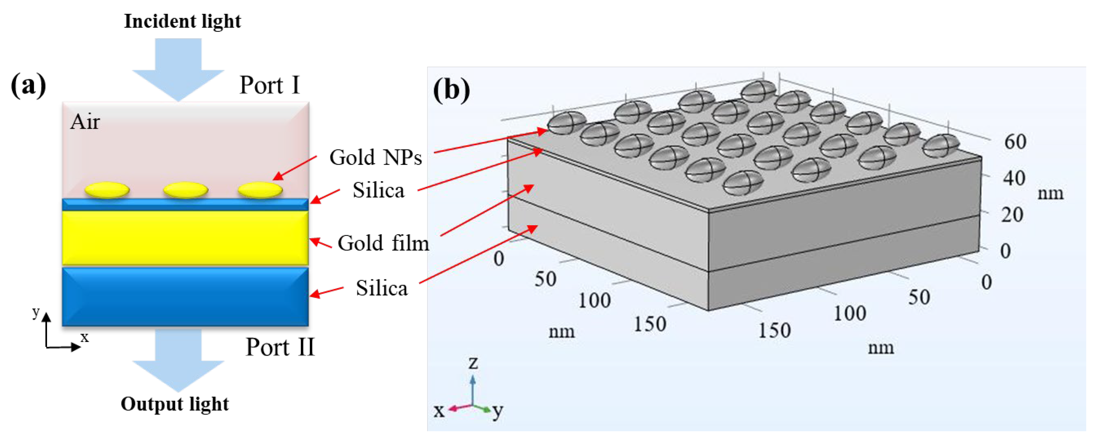
In this study, we have tried to overcome some of these challenges by designing a simple structure shown in
Figure 1. In this configuration, LSPRs will be induced with a normal external electric field incident from the top of the structure. Therefore, controlling the incident light angle will not be a problem. In this work, the main purpose is coupling the NPs to their induced dipole image in the metal film. In this regard, particles separation plays a crucial role on the resulting field enhancement in the dielectric layer between the NPs and metal film. While there is not too much attention to this important factor in related works and it has not been categorized as an effective parameter. More precisely, a larger separation distance compared to the size of the NPs can reduce the probability of the LSPR coupling between the particles. It solves the mentioned problem of controlling separation distance in the case of short distances. Therefore, to optimize the separation distance of the NPs, normal components of the electric field along various cutlines through the structure and for different particle separations have been studied by considering metal film and metal NPs made of gold. Due to the importance of silver NPs in the plasmonic field of research, the same study is performed for a certain separation distance of the metal NPs while gold is replaced with silver as a metal film and metal NPs. The optical response of the structure with silver as a metal film and gold as NPs is also explored to achieve the best combination with the strongest field enhancement in the gap film. The proposed structure has potential application as plasmonic-receiving nano antennas due to the strong absorption and enhancement of the incident light into an ultrathin dielectric layer. This characteristic feature also leads to a high-quality Raman spectrum, making this structure promising as a SERS platform. Moreover, due to the strong field enhancement in the dielectric layer, a change in the refractive index of the dielectric or geometrical parameters of the layer could lead to a change in the resonance frequency of the structure, which is promising for sensing applications.
3. Result and Discussion
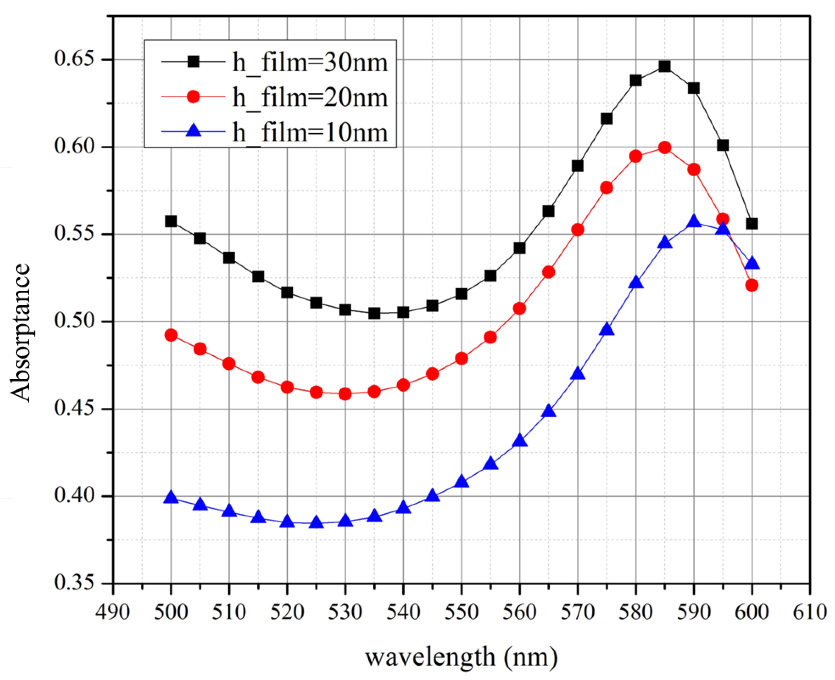
To study the influence of the metal film thickness on the resonance wavelength, the absorptance spectrum of the structure is derived in the graph in
Figure 2 for different thicknesses of 10 nm, 20 nm, and 30 nm. It demonstrates that decreasing the thickness from 30 nm to 20 nm leads to a decline in total absorptance, as expected. However, this thickness modification does not significantly affect the resonance wavelength of the structure. Decreasing the thickness from 20 nm to 10 nm, which is less than the dimension of the metal NPs, leads to the resonance wavelength shift to longer wavelengths by 5 nm.
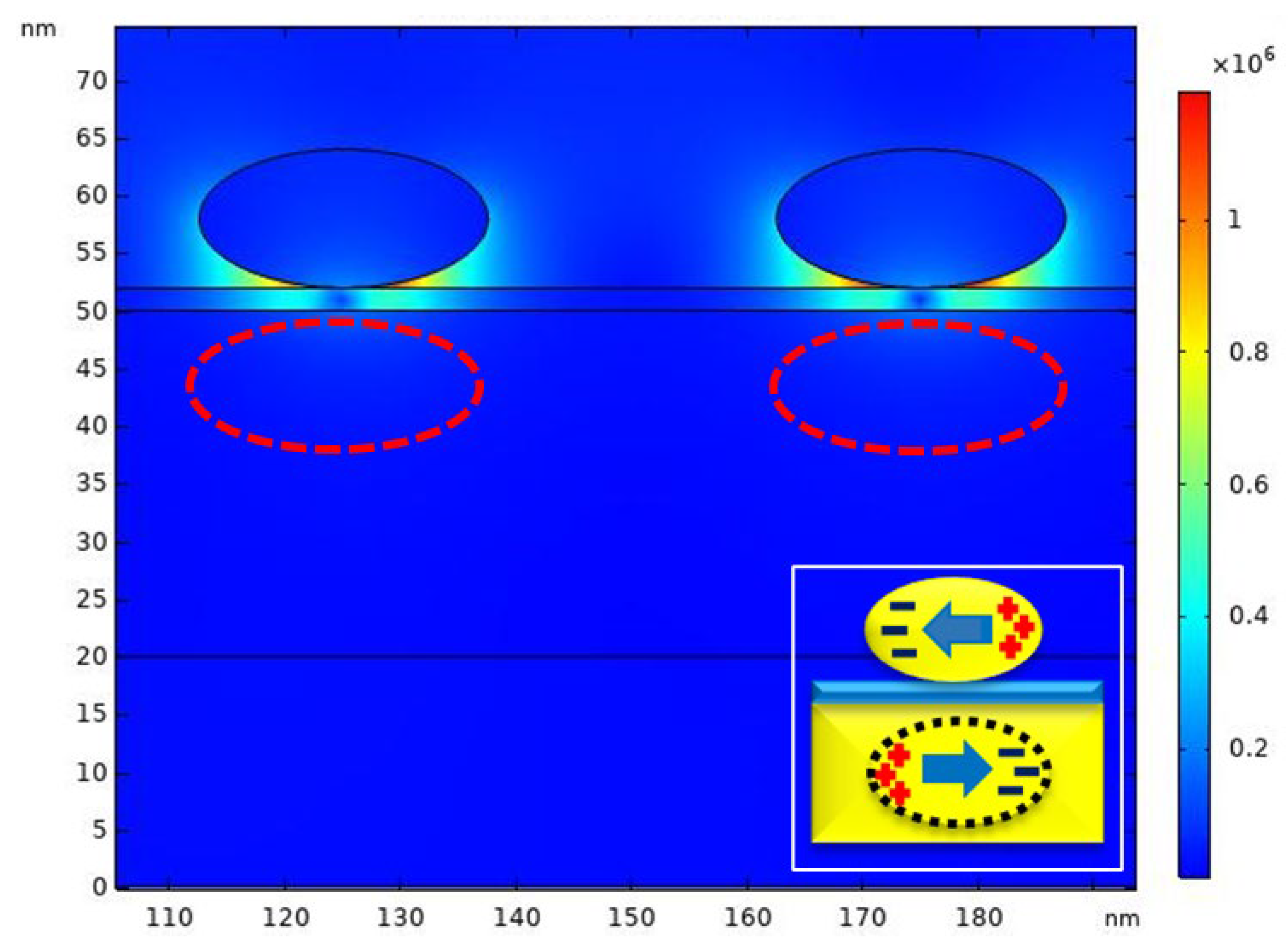
Figure 3 indicates the distribution of the normal component of the electric field in the y direction in the proposed structure at resonance wavelength (λ = 585 nm) which is derived from
Figure 2 for 30 nm metal film thickness. The thickness of the dielectric layer is 2 nm, and the separation distance of the particles is 20 nm. The main goal of this study is the coupling strength between the metal film and NPs which is the reason for the adoption of declared separation between the particles. In other words, the separation distance must be large enough compared to the dielectric layer thickness to decrease the effect of the coupling between the LSPRs of the particles. Purpose coupling will be established in the dielectric layer, as obvious in
Figure 3, in the shape of hot spots in that area. Two ellipses drawn with red dashed lines in the metal film represent the induced image of the particles. These induced images have opposite dipole with the real particles dipole, as shown in the inset picture inside
Figure 3.
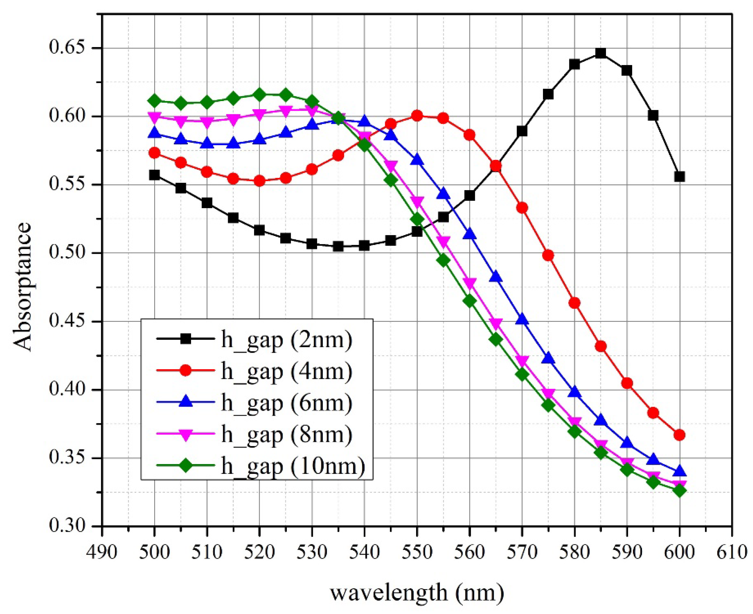
As mentioned in all the previous written works in this field of research, the thickness of the dielectric layer plays an important role in the plasmonic properties of such structures. To observe this effect on the resonance wavelength of the LSPRs, the gap layer thickness was decreased from 10 nm to 2 nm for the proposed wavelength range shown in
Figure 4. As obvious, by decreasing the thickness, the resonance wavelength is shifted to the longer wavelengths, and the FWHM of the absorptance peak is smaller, which is beneficial for sensing applications.
To achieve strong LSPR and, consequently, strong field enhancement in the dielectric layer, nanoparticle separation should be large enough compared to the gap layer thickness.
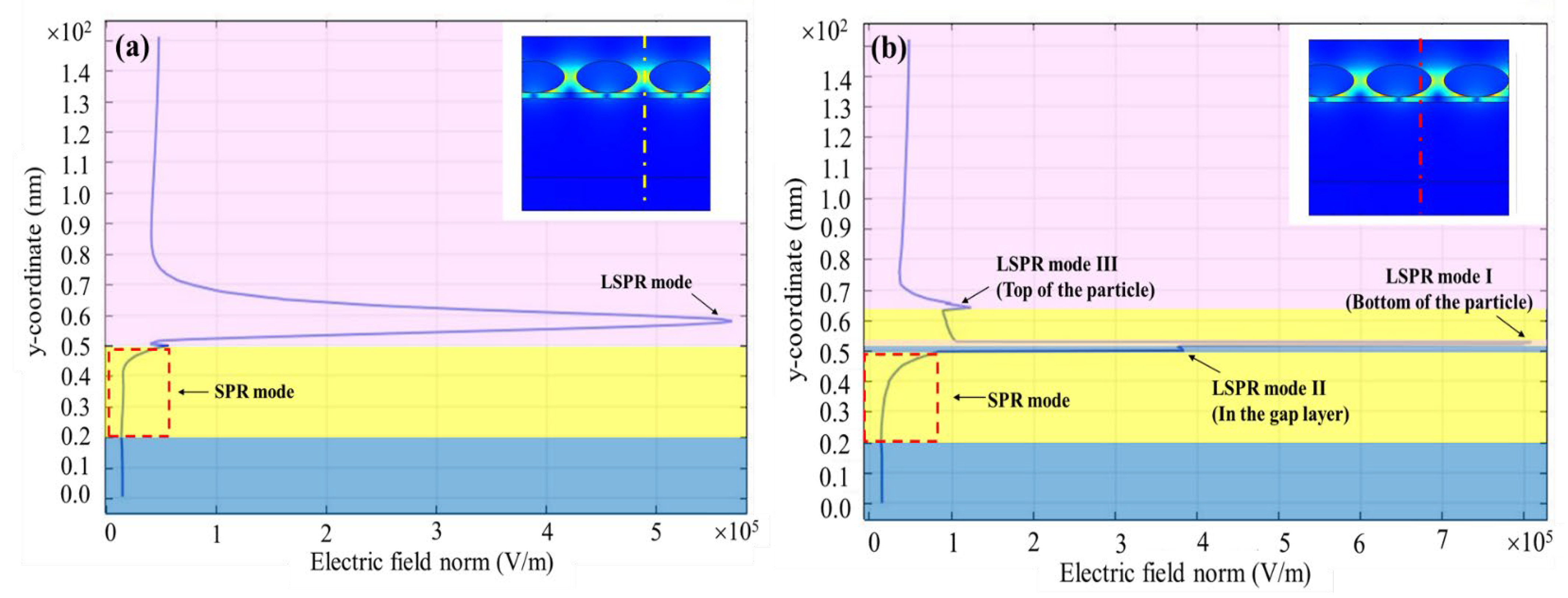
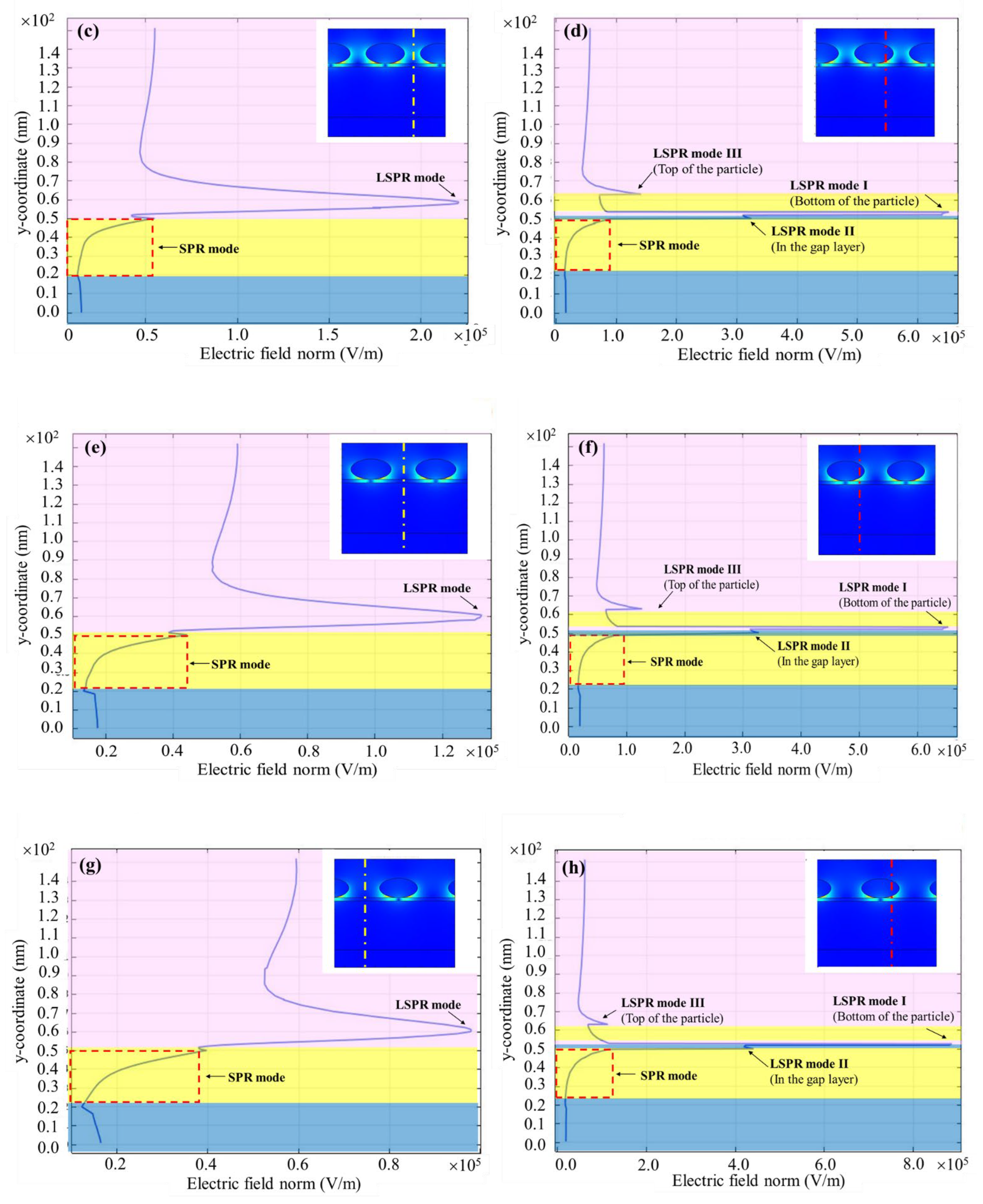
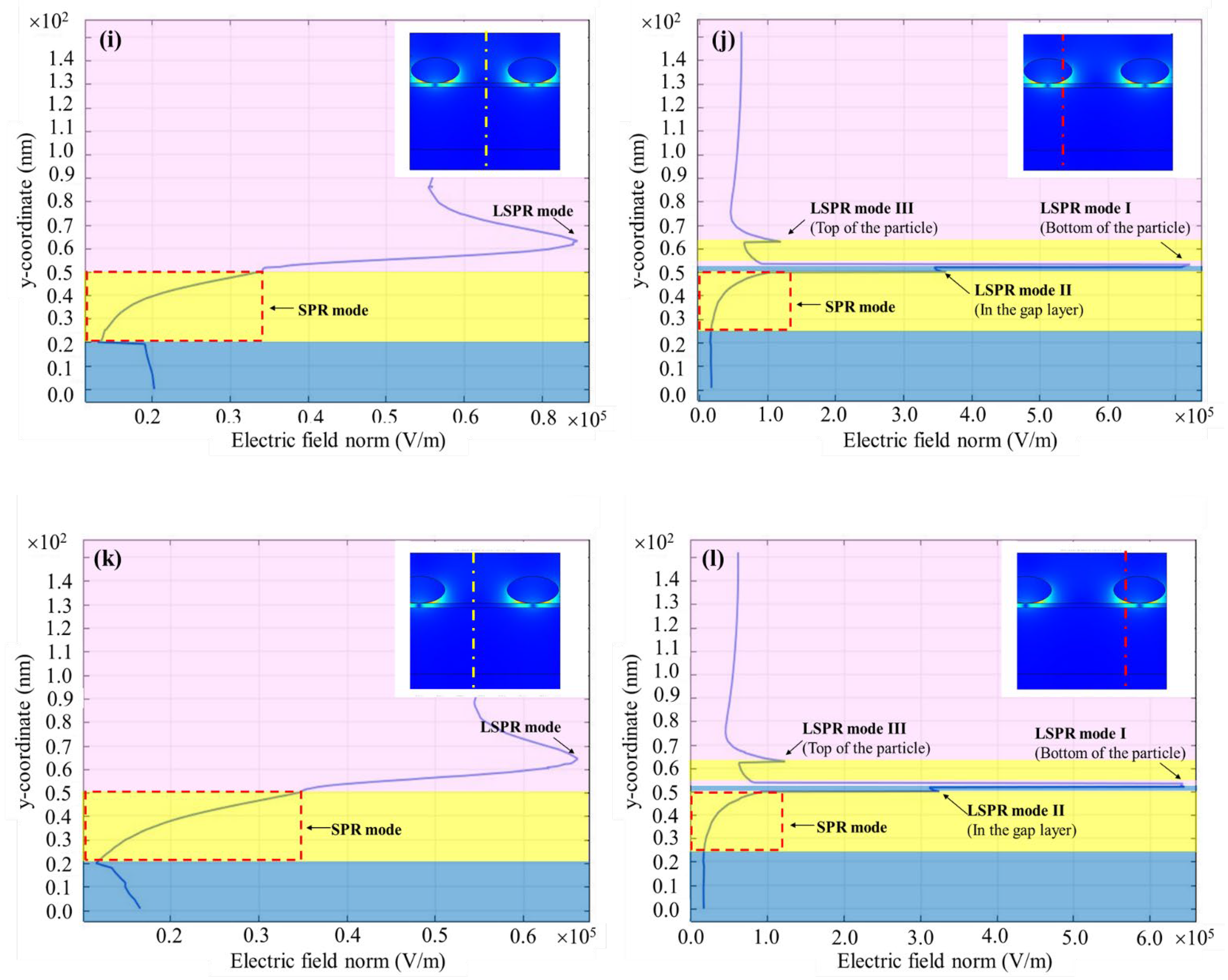
Figure 5 shows simulation results for particle separations varied from 5 nm to 30 nm, where a normal component of the electric field in the y direction is studied. In each pair of graphs (for instance, a and b), different field distributions for the same particle separation but along different axes are demonstrated, as explored in inset pictures (along dashed yellow and red lines). As shown in
Figure 5a, when particle separation is as small as the dielectric layer thickness, LSPR coupling between the particles plays an important role. Another point in this picture is the induction of the SPR at the interface of the metal film and dielectric layer, which decays by increasing the distance from the interface, as expected. However, this SPR mode is insignificant compared to the LSPR mode between the particles. Comparing the graphs in
Figure 5a,b shows the electric field in the dielectric layer due to the coupling of the LSPR mode II of the particle. Its dipole image in
Figure 5b is not as strong as the electric field between the particles shown in
Figure 5a. A closer look at the graph in
Figure 5b reveals that two LSPR modes are also obvious in the inset picture, as two hot spots at the bottom of the particle and in the gap layer are visible. The graphs indicate that the normal component of the electric field intensity related to the LSPR mode I is stronger than LSPR mode II. Maxwell’s continuity conditions could explain the reason. Based on these continuity conditions, the normal component of the electric displacement (
requires continuing across the interface between two materials. Consequently, the normal component of the electric field in the air will be larger than its value in the dielectric layer by a factor approximating the dielectric constant of the dielectric layer material. This can describe the reason for the compression in the size of the hot spot in the dielectric layer as compared to the region between the dielectric layer and NPs. However, even the maximum electric field intensity related to the LSPR mode I in
Figure 5b is still very close to the maximum electric field in the separation distance of the particles in
Figure 5a. To enhance the electric field in the gap layer, the separation distance is increased from 5 to 10, 15, 20, 25, and 30 nm, and the results are shown in
Figure 5c–l. Increasing the separation distance decreases the electric field between the particles related to the LSPR coupling of the particles.
On the other hand, the electric field in the dielectric layer and from its interface to the bottom of the particle (along the yellow dash line passing through the particle) is increased in both cases until the separation distance of 20 nm. It begins to decline after increasing the separation from 20 nm to 30 nm by a factor of 2 × 10
5 V/m. This declining trend after 20 nm might be due to the possibility of considering NPs as single particles when they have a very large separation distance (more than 20 nm). Accordingly, the influence of more than one nanoparticle in field enhancement is larger than that of a single nanoparticle. By increasing the separation distance of the particles, the normal electric field related to the SPR mode at the metal-dielectric interface along the axis passing through the separation distance of the particles is decreased from 9 × 10
4 V/m to 6 × 10
4 V/m. This decreasing trend might be because, in the case of smaller separation, the particles can be considered as an array that fulfills the coupling condition needed for the excitation of the SPRs. By increasing the separation of the particles, each particle can be considered as a single particle, and the probability of the SPR induction is decreased. However, this increasing separation does not significantly affect the electric field’s normal component related to the SPR mode, along the axes passing through the particles and it remains around 10
5 V/m. The reason might be related to the important role of the LSPRs in the dielectric layer. LSPR mode III in
Figure 5b,d,f,h,j,l represents the LSPR mode on the top of the particles, which is not coupled and declined by increasing separation of the particles.
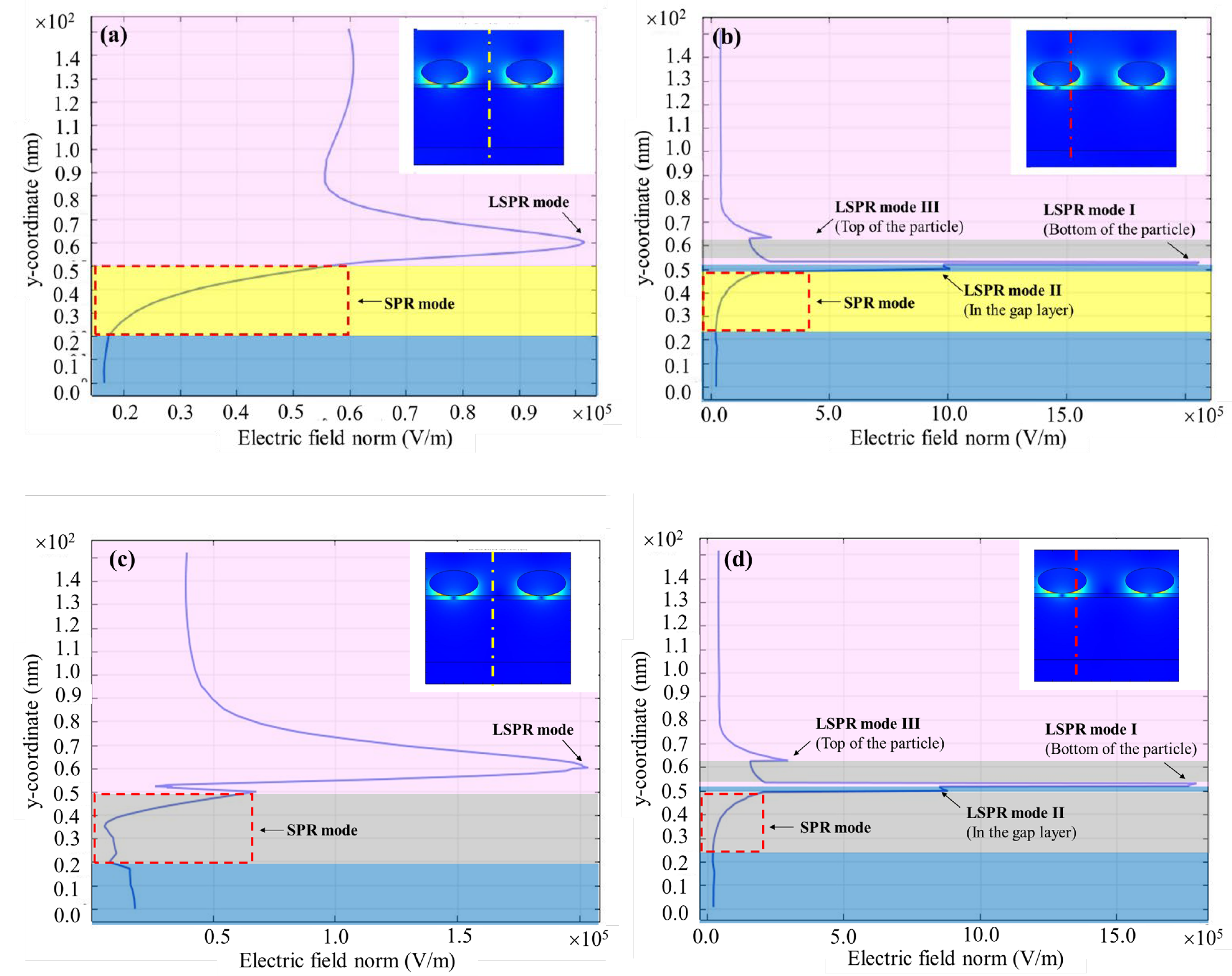
To study the influence of using silver instead of gold in the proposed structure, the same simulation, as in
Figure 5, is performed for two cases of using silver as metal NPs and gold as metal layer and silver as both metal layer and metal NPs. The results are presented in
Figure 6a–d. In both cases, the particle separation is set to 20 nm. The electric field intensity is measured at the resonance wavelength of the structure, which is 565 nm for the structure with gold NPs and silver metal layer (
Figure 6a,b) and 480 nm for silver NPs and metal layer(
Figure 6c,d). A comparison of
Figure 5g and
Figure 6a shows that utilizing the silver layer instead of the gold layer leads to increasing of the normal component of the electric field related to SPR mode in the metal-dielectric interface from 0.4 × 10
5V/m to 0.6 × 10
5V/m, where the electric field is measured along the axis passing through the middle of the particle separation. In the case of the electric field related to the LSPR coupling between the particles, this increasing trend is from 0.985 × 10
5V/m to 1.085 × 10
5V/m. Therefore, utilizing the silver layer could lead to a stronger SPR mode in the metal-dielectric interface and stronger LSPR coupling between the particles. However, a comparison of
Figure 5h and
Figure 6b does not give the same result for the field enhancement in the dielectric layer. The maximum normal component of the electric field related to the LSPR mode II in
Figure 5h is larger than 3.95 × 10
5 V/m, while it is 1.485 × 10
5 V/m in
Figure 6b.
The graphs in
Figure 6c,d show electric field distribution along different axes when using silver instead of gold as metal film and NPs. As shown in
Figure 6c, the normal component of the electric field related to the SPR mode in the metal–dielectric interface is around 0.7 × 10
5V/m, while this electric field is around 0.4 × 10
5V/m in
Figure 5h. To compare the LSPR coupling strength between the particles of silver and gold, it is obvious that utilizing a configuration with silver NPs and the silver film could be more effective in field enhancement in the separation distance of the particles. Since the normal component of the electric field along axes passing through the middle of the separation distance of the particles increased from 0.985 × 10
5V/m in
Figure 5h to 2.04 × 10
5V/m in
Figure 6c.
The graphs in
Figure 5h and
Figure 6d give the needed information for comparing the effect of replacing gold with silver on the field enhancement in the dielectric layer. As shown in these Figures, the normal component of the electric field along axes passing through the particle related to the LSPR mode II is increased from 3.95 × 10
5 to 1.005 × 10
6V/m by replacing gold with silver.
Despite this work being simulation research, it is worth suggesting some fabrication methods which propose for future works. In line of this perspective, metal film could be deposited on the substrate by electron beam evaporation or thermal evaporation method as it was done in references [
1,
17,
27,
28]. The dielectric layer between the metal film and metal NPs could be a monolayer of dielectric quantum dots, which could be deposited by drop casting of the solution containing a special concentration of the quantum dots [
17]. A dielectric layer could also be deposited on the metal film by evaporation methods [
28]. In the case of using Silica and gold as dielectric and metal film, an ultrathin Cr adhesion layer could be utilized to prevent common adhesion problems between gold and Silica [
28]. The next step in fabrication is related to synthesizing metal NPs on the dielectric layer. In this case, the most common and effective method for synthesizing metal NPs is the seed-mediated method [
29]. Afterward, the NPs dispersed in ethanol suspension could be coated on the dielectric layer by drop-casting method [
25].
Table 1 gives a comparison of the present structure and the other recent related structures in the literature by comparing the conditions needed for the induction of the LSPRs in each structure. As demonstrated in this table, different types of structures with different nanostructures including NPs (spherical, elliptical, etc.), nanorods (NRs), nanocubes (NCs) and nanodisks (NDs) are compared. As mentioned in the introduction, exciting the LSPRs in such structures face some limitations, including angle tuning, polarized incident light, and needed coupling configuration.
Table 1 shows the presented structure has no limitation, since the incident light could be normal visible light, at a direct angle. Moreover, it needs no coupling configurations such as a prism, grating, or waveguide coupling which are complicated.


